
Volume: 11 Issue: 08 | Aug 2024 www.irjet.net p-ISSN: 2395-0072

Volume: 11 Issue: 08 | Aug 2024 www.irjet.net p-ISSN: 2395-0072
Ayush Tiwari1 , Keshav Lavania2 , Jai Kashmira3 , Jatin Rana4
1,2,3,4B. Tech, ECE, G.B Pant Institute of Engineering and Technology, Pauri, India
Abstract - ThismanuscriptexploresthesimulationofatrigateJunctionless AccumulationMode Field-EffectTransistor (JLAM-FET) in Silvaco, conducting an analysis to calculate sensitivity while varying permittivity concerning shifts in parameters such as threshold voltage, charge, doping concentration,andchannellength,specificallyinthecontext of biomolecules. Unlike a traditional Metal-OxideSemiconductor Field-Effect Transistor (MOSFET), a junctionlesstransistorlacksjunctions,anditscurrentdriveis regulated by doping concentration rather than gate capacitance. Notably, a Junctionless transistor exhibits superior performance compared to a conventional MOSFET, particularly in scenarios with a short channel length. An optimal doping concentration of 1 × 10^18 cm⁻³ and a thresholdvoltagechangeof2000mVareidentifiedtoachieve maximumsensitivity.Thealterationinthecentralpotentialof thechannelemergesasacriticalfactorindeterminingboth threshold voltage and device sensitivity. The successful simulationofthedevicecapturesallvariationsandoutcomes. As we navigate through the intricate landscape of semiconductor physics and biomolecular interactions, the findings not only solidify the JL AM-FET's standing as a forefront technology but also open avenues for tailoring its capabilitiestospecificbiomolecularsensingapplications.This holistic approach contributes to the growing body of knowledge in semiconductor device engineering, presenting opportunities for the development of innovative solutions in biosensingtechnology.
Key Words: Short channel effects, Central potential alteration, Current drive, Central potential alteration, Channel length, Permittivity variation, Sensitivity analysis.
Biosensors are crucial tools for the rapid detection of biomolecules, with a particular promise in label-free detectionofbothneutral(biotin–streptavidin)andcharged biomolecules (DNA). The advancement in fabrication technologies has facilitated the cost-effective large-scale production of nanoscale biosensors, which are compatible with CMOS (Complementary Metal Oxide Semiconductor) technology. This integration streamlines the detection systems,eliminatingtheneedforcomplextransducersand pavingthewayforsystem-on-chip(SoC)applications.
Among the different types of biosensors developed, including optical, electrochemical, nano-mechanical devices, ion-sensitive electrodes, and piezoelectric models, Field Effect Transistor (FET)-based biosensors have gained widespreadadoption.
Junctionless field-effect transistors (JLFETs) are emerging as promising devices due to their simpler fabrication process, which omits the need for conventional p-n junctions, enabling further device miniaturization. These transistors offer a high ION/IOFF ratio, minimal thermal budgeting, near-ideal subthreshold swing, and reduced roll-off. However, JLFETs face challenges such as mobility degradation due to heavily doped channels and reduced ON current(ION)causedbyhighparasiticresistances.
To address these issues, Junction Accumulation Mode (JAM) FETs have been introduced. They maintain heavy doping in the source/drain regions while lowering the channel doping, enhancing both ION and the ION/IOFF ratio compared to traditional JLFETs. However, high electric fields at the channel/draininterfaceduringtheONstatecanleadtohotelectron effects (HCEs) and gate-induced drain leakage (GIDL).Dual-materialgateengineeringisaprovenmethodto counteract these reliability issues, as well as short- channel effects(SCEs),invariousFETarchitectures.
Additionally, the Tri-Gate (TG) architecture has gained attention for its excellent gate control in sub-100 nm regimes, making it highly effective in mitigating SCEs and conducting higher currents than double-gate MOSFETs (DGMOSFETs). The feasibility of fabricating both n-channel and p-channel TG MOSFETs underscores its potential for realworldapplications.Tri-Gatedevices areknownfortheir high ION/IOFF ratio and power efficiency, making them more power-efficient than other FET types, including planar or FinFETs. Features like reduced surface scattering, improved subthreshold swing (SS), and lower drain-induced barrier lowering (DIBL) make TG-JLFETs particularly suitable for both analog and digital applications. The TG-JLFET architecture's enhanced gate-channel electrostatics offer immunity toSCEs,pushingtheboundaries ofdevicescaling. With increasing demand for high packing density, managing short-channel effects and parasitic capacitances, such as those addressed by Silicon-on-Insulator (SOI) technology, becomescrucial.
International Research Journal of Engineering and
Volume: 11 Issue: 08 | Aug 2024 www.irjet.net
TheoperationofaJunctionlessfield-effecttransistor(JL-FET) is based on the modulation of the conductive channel between the source and drain regions by the electric field appliedbythegateelectrode.Unliketraditionalfield-effect transistors(FETs),JL-FETsdonotrelyonajunctionbetween different semiconductor materials for their operation. Instead,theentirechannelisuniformlydoped,andthegate voltagedirectlyinfluencestheconductivityofthechannel.
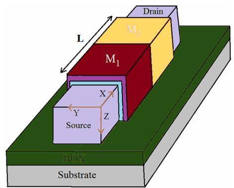
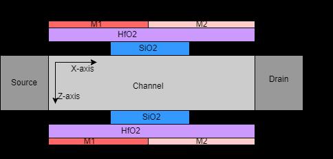
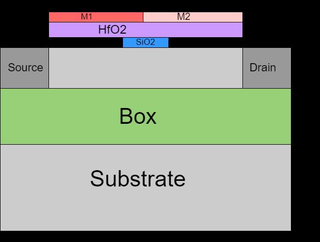
The 3-D structure of a Tri-Gate Junctionless Field-Effect Transistor(JLFET)isillustratedinFig.1(a).Thetopviewof the device, as shown in Fig. 1(b), reveals a symmetric double-gate configuration, while the side cross-sectional view, depicted in Fig. 1(c), presents the device as an asymmetricSilicon-On-Insulator(SOI)structure.Thesilicon film is enveloped on three sides by stacked oxide layers HfO2 on top of cavities and SiO2 with respective thicknessestHfO2andtSiO2,maintaininganeffectiveoxide thickness(EOT)oftOX.Thegateisformedusingtwometals withdifferent work functions(φM1and φM2).Thedevice features varying donor densities in the channel and source/drain(S/D)regions,withtheS/Dregionsdopedata higherlevel(NSD)andthechanneldopedataslightlylower concentration(NC)ofthesametype.Thechannel'slength, width,andthicknessareorientedalongthex,y,andz-axes, respectively.
The proposed device has been analytically modelled with specific geometrical constraints: i) the thickness of the buried oxidelayer(tbox) mustbegreater than or equal to thechannellength(L)tominimizeinteractionbetweenthe twosidegates;ii)thechannellengthshouldbeatleasttwice thewidth/thicknessofthedeviceormore,i.e.,L≥2WandL
≥2tsi.Thechannelpotential[ψ(x,y,z)]atanygivenpointis represented using a perimeter-weighted sum approach, combining ψ(x,y) and ψ(x,z). These are the potential functions for the symmetric double-gate structure and the asymmetric SOI device, respectively, derived from the analyticalmodelbysolvingthe2DPoisson’sEquation.
1.3
The performance of the Dual-material Tri Gate JLFET is significantly influenced by several critical parameters. The channel length (L) determines the distance between the source and drain regions, impacting the device’s currentcarrying capability and overall conductance. For effective short-channel performance, the channel length is carefully designed to be at least twice the channel width (W) and thickness (tsi), ensuring minimal interaction between the sidegates.Thechannelwidth(W)and thickness(tsi)arealso crucial, as they affect the electrostatic control and current flow through the channel. The gate oxide thickness (tox) plays a pivotal role in defining the gate capacitance and control over the channel, with a balance needed between performance enhancement and gate leakage.The thickness of theburiedoxidelayer(tbox)ischosento begreaterthanor equal tothechannel length to reduce theinteraction between thesidegates.Dopingconcentrationsinthesourceanddrain regions, as wellas thechannel, areoptimized to enhance the ON current (ION) and the ION/IOFF ratio. The gate is constructed using metals with distinct work functions (φM1 and φM2), which influence the threshold voltage and device characteristics. Additionally, the gate oxide comprises stacked layers of high-K dielectric material (HfO2) and SiO2,
International Research Journal of Engineering and Technology (IRJET) e-ISSN: 2395-0056
Volume: 11 Issue: 08 | Aug 2024 www.irjet.net p-ISSN: 2395-0072
with their respective thicknesses (tHfO2 and tSiO2) optimizedtominimizesurfacescatteringandgateleakage
whilemaintainingthe effectiveoxide thickness (EOT) The orientationofchanneldimensionsalongthex,y,andzaxes affectsthedevice’sspatialcharacteristicsandperformance Managing parasitic capacitances, often through techniques likeSilicon-on-Insulator(SOI)technology,isalsocrucialfor improvingtheswitchingspeedandoverallefficiencyofthe device.Eachoftheseparametersplaysavitalroleindefining the functionality and efficiency of the device, and their careful optimization is essential for achieving highperformanceField-EffectTransistors.
AllsimulationsareconductedusingtheSilvacoATLASdevice simulator,employingstandarddensitymodels Theprimary modelsutilizedinthesimulationincludetheDrift-Diffusion model, theShockley-Read-Hall (SRH)recombination model, andtheLombardiMobilityModel Arobustmeshingstrategy is implemented to ensure precision Empirical parameters incorporatedintothemodelaresourcedfromreferences.The body (substrate) and source terminals are connected to groundtocompletethecircuit.
Table -1: Devicedimensionsandbiasingvoltagesusedfor simulations
Parameters
High-Koxidelayerthickness(tHfO2) 2nm
ThicknessofSilicondioxide(tSiO2) 1nm
Work-functionsofdualmetalgate(φM1, φM2) 47eV,52eV
Channeldoping(NC)
1018 cm-3
Channellength(L) 30nm
Source/Draindoping(NSD) 1020cm-3
Thicknessoftheburiedoxidelayer(tbox) 60nm
ThicknessandwidthofSi-film(tSi,W) 10nm,10nm
Gatevoltage(Vgs),DrainVoltage(Vds) 0-2V,08V
Sensitivityisacrucialparametertoconsiderwhileevaluating a biosensor’s effectiveness. The Dual-material tri gate JLFET’s sensitivity is assessed based on changes in electricalcharacteristics(I&V)broughtonbyvariationsin thetargetbiomolecule’srelativedielectricconstantstothe airin the nanogapcavity.Inthisworkthethresholdvoltage sensitivity (SVth) is taken into account to assess its performance.Anditcanbecalculatedas:
SVth = Vth(bio) – Vth(air) Vth(air)
where,
Vth(bio)- Threshold voltage for a certain biomolecule in the cavity
Vth(air)-Thresholdvoltageforairinthecavity
2.1 Result
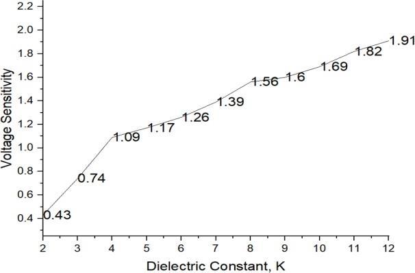
Fig.2(a): VoltageSensitivityalongthechangingdielectric constant
Figure 2(a) clearly demonstrates that an increase in the dielectricconstantwithinthenanogapcavityregionresultsina significant enhancement in the voltage sensitivity of the device.Thisobservationunderscoresthecriticalrolethat the dielectric environment plays in determining the device's sensitivity to voltage changes. As the dielectric constant withinthenanogapcavity is increased, thedeviceexhibits a marked improvement in its voltage sensitivity, which directly influences its ability to detect and respond to minute variations in electrical signals. This enhanced sensitivity is particularly important for applications requiring precise measurement and detection, as it enables the device to discern smaller changes in voltage more effectively. The relationship between the dielectric constant and voltage sensitivity highlighted in the figure illustrates the potential for optimizing device performance through adjustments in the dielectric environment, ultimately leading to improved accuracyandreliabilityinitssensingcapabilities.
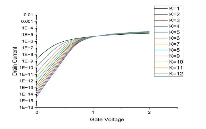
Fig.2(b):DrainCurrentVSGateVoltage
International Research Journal of Engineering and Technology (IRJET) e-ISSN: 2395-0056
Volume: 11 Issue: 08 | Aug 2024 www.irjet.net
Figure 2(b) illustrates that an increase in the dielectric constantwithinthenanogapcavityregionofthedeviceleads toacorrespondingriseinthethresholdvoltage.Thiseffectis crucial in understanding how variations in the dielectric environmentimpacttheperformanceoftheJunctionlessFETbasedbiosensor.Specifically,whenthedielectricconstant(K) is altered, the device's threshold voltage changes significantly.Inthecontextofthebiosensor'soptimaldoping concentration,setat1×10^18cm⁻³,thechangeinthreshold voltageisnotablypronounced.FordielectricconstantsofKfilled = 1 and K-filled = 12, the threshold voltage variation amounts to 400 mV. This substantial shift highlights the sensitivity of the device to changes in the dielectric environment, which is a critical factor in enhancing the biosensor'sdetectioncapabilities.Theabilityofthedeviceto exhibit such a pronounced response to dielectric changes underlines its potential for precise biomolecule sensing applications,where even minor variationsin thedielectric constantcanbedetectedandquantified.Thischaracteristic makestheJunctionlessFET-basedbiosensorapromisingtool foradvancedsensingtechnologies,wherehighsensitivityand accuracyareessential.
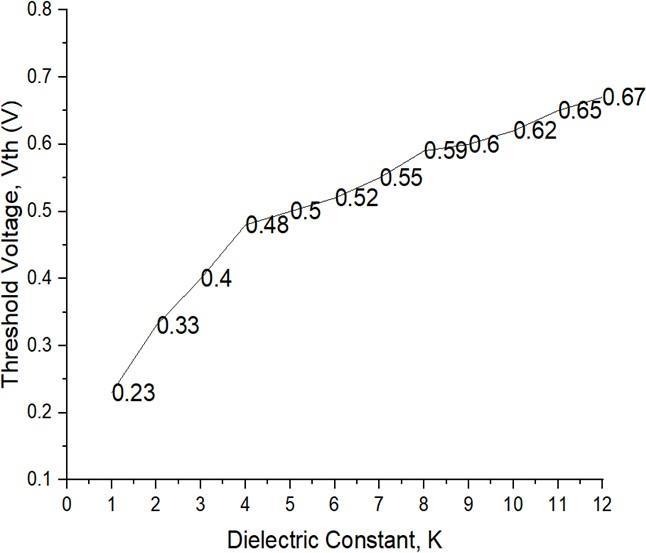
Fig.2(c):ThresholdVoltageVSDielectricConstant
It can be seen that VTH increases with rise in k due to reductioninID.Itisobservedthattheproposedbiosensor gives better discrimination among biomolecules at lower values of k whereas the discriminability of sensor sharply decreaseswithincreaseink.Thisisduetothefactthatthe changeinVTH islesserforhighervaluesofk.Therefore,the proposedbiosensorishighlyselectiveforlowervaluesofk.
In this study, we investigated the performance of a DualmaterialtrigateJLFET forbiomoleculesensing,utilizing simulations conducted in the Silvaco ATLAS device simulator. Our analysis focused on how variations in dielectric constant withinthenanogapcavity affectcritical parameters such as threshold voltage and voltage sensitivity.
Thefindingsrevealedthatanincreaseindielectricconstant significantly enhances both the threshold voltage and voltagesensitivity,demonstratingthedevice'spotentialfor high-sensitivitybiomoleculedetection.
TheDual-materialtrigateJLFETdesign,characterizedby an optimal doping concentration of 1 × 10^18 cm⁻³, exhibited a notable change in threshold voltage, when transitioning from dielectric constants of K-filled = 1 to Kfilled=12.Thissubstantialsensitivitytodielectricchanges underscores the device's suitability for applications requiring precise detection of biomolecular interactions. Furthermore, the implementation of robust meshing strategiesandstandarddensitymodels,includingtheDriftDiffusion model, SRH recombination model, and Lombardi MobilityModel,ensuredaccuratesimulationresults.
Overall, the Dual-material tri gate JLFET presents a promising platform for label-free biosensing, offering significant advantages in sensitivity and simplicity over traditionalbiosensors.Thestudyhighlightstheimportance ofoptimizing dielectric environmentsanddeviceparameters to achieve enhanced performance in semiconductor-based biosensors.Futureworkcouldexplorefurtherrefinementof thedevicestructureandtheintegrationofadditionalsensing modalities to expand its applicability in biomedical and environmentalmonitoring.
We would liketo thank the Department ofElectronicsand Communication Engineering, G.B Pant Institute of Engineering and Technology Pauri for their constant support.
[1] Sahay S, Kumar MJ (2017) Symmetric operation in an extendedbackgateJLFETforscalingtothe5-nmregime considering quantum confinement effects. IEEE Trans Electron Devices 64(1):21–27. https://doi.org/10.1109/TED.2016.2628763
[2] Dash S, Mishra GP (2016) An extensive electrostatic analysis of dual material gate all around tunnel FET (DMGAA TFET). Adv Nat Sci: Nanosci Nanotechnol 7(025012).https://doi.org/10.1088/20436262/7/2/025012
[3] SinghB,GolaD,SinghK,GoelE,KumarS,JitS(2017)2DAnalyticalthresholdvoltagemodelfordielectric pocketdouble-gateJunctionlessFETsbyconsidering source/draindepletioneffect.IEEETransElectron Devices 64(3):901–908.https://doi.org/10.1109/TED.2016.2646460
[4] PratapY,HaldarS,GuptaRS,GuptaM(2015)Localized charge dependent threshold voltage analysis of gate-
International Research Journal of Engineering and Technology (IRJET) e-ISSN: 2395-0056
Volume: 11 Issue: 08 | Aug 2024 www.irjet.net p-ISSN: 2395-0072
material-engineered junctionless nanowire transistor. IEEE Trans Electron Devices 62(8):2598–2605. https://doi.org/10.1016/j.aeue.2019.06.017
[5] MagnoneP, Crupi F, Giusi G, PaceC, SimoenE, Claeys C, Pantisano L, Maji D, Rao VR, Srinivasan P (2009) 1/f NoiseindrainandgatecurrentofMOSFETswithhigh-k gate stacks. IEEE Trans Device Mater Reliab 9(2):180–189.https://doi.org/10.1109/TDMR.2009.2020406
[6] S. Kanungo, S. Chattopadhyay, P. S. Gupta, K. Sinha, and H. Rahaman, “Study and analysis of the effects of SiGe source and pocket-doped channel on sensing performance of dielectrically modulated tunnel FETbasedbiosensors,”IEEETrans.ElectronDevices,vol.63, no.6,pp.2589–2596,Jun.2016.
[7] A. Chakraborty, D. Singha, and A. Sarkar, “Staggered heterojunctions-based tunnel-FET for application as a label-freebiosensor,”Int.J.Nanoparticles,vol.10,nos. 1–2,pp.107–116,2018.
[8] https://doi.org/10.22034/ijnd.2021.681554
Aditya M, Srinivasa Rao K, Sravani K, Guha K (2021) Design, simulation and analysis of high-K gate dielectric FinField effect transistor. International JournalofNanoDimension 12(3):305 309.
[9] LöfflerG,SchreiberH,SteinhauserO(1997)Calculation ofthedielectricpropertiesofaproteinanditssolvent: theoryandacasestudy.JMolBiol270(3):520–534.
[10] Auth C, Plummer JD (1998) A simple model for threshold voltage of surrounding-gate MOSFET’s. IEEE Trans Electron Dev 45(11):2381–2383. https://doi.org/10.1109/16.726665,2381
[11] https://doi.org/10.1109/TED.2003.821384
ZhuW,HanJ,MaTP(2004)Mobilitymeasurementand degradation mechanisms of MOSFETs made with ultrathinhigh-kdielectrics.IEEETransElectronDevices 51(1):98–105.
[12] Houssa M, Pantisano L, Ragnarsson ˚ AL, Degraeve R, Schram T, Pourtois G, De Gendt S, Groeseneken G, HeynsMM(2006)Electrical properties of high-k gate dielectrics: challenges, current issues, and possible solutions. Mater Sci Eng 51(4- 6):37–85. https://doi.org/10.1016/j.mser.2006.04.001