
International Research Journal of Engineering and Technology (IRJET) e-ISSN: 2395-0056
Volume: 11 Issue: 08 | Aug 2024 www.irjet.net p-ISSN: 2395-0072

International Research Journal of Engineering and Technology (IRJET) e-ISSN: 2395-0056
Volume: 11 Issue: 08 | Aug 2024 www.irjet.net p-ISSN: 2395-0072
Sahana J K1, Dr. Anitha G S2, T K Nagaraju3, Bhoopendra Kumar Singh4
1P G Student, RV College of Engineering, Bengaluru
2Associate Professor, RV College of Engineering, Bengaluru
3Assistant Manager, Centum Electronics Limited, Bengaluru
4Director, Centum Electronics Limited, Bengaluru
Abstract This paper focuses on the design of a forward converter for space application to solve major problems in power management, efficiency, and reliability. The converter uses advanced technology to ensure stable operation in harsh environments. It incorporates key features such as EMI filtering, radiationhardened components, and thermal management systems to ensure durability in space. It includes a current transformer for sensing, an input under-voltage shutdown for protection, and a feedforward and PWM controller for output regulation. Magnetic Amplifiers and Optocouplers provide additional stability and isolation. Future advancement includes Al-driven control, and costeffective, eco-friendly designs. Simulation and testing will demonstrate the converter’s performance, ensuring it meetsthespacemissionrequirements.
Index Terms EMI, Magnetic Amplifiers, Optocouplers, PWMcontroller,feedforward.
THE design of power supplies is a crucial factor in determining the performance, efficiency, and reliability ofmodern electronicdevices[1].Amongthe various power supply configurations, Switched-Mode Power Supplies (SMPS) have gained widespread adoption due to their superior efficiency,compactdesign,andadaptabilityto variousapplications. SMPS technologyis utilized ina variety of electronic systems, ranging from consumer electronics to industrialequipment,owingtoitsabilitytoconvertelectrical powerwithminimalenergylossefficiently[2].
ThispaperanalyzesSMPSarchitecturein-depth,emphasizing theessentialfunctionalblockscontributingtoitsoperation.It outlines the core components, including the Electromagnetic Interference (EMI) filter, rectification and filtering stages, Pulse Width Modulation (PWM) control, and output regulation circuits. The EMI filter is vital in reducing noise emissions, and ensuring compliance with electromagnetic
compatibility standards [3]. The rectification and filtering stagestransformtheACinputintoastableDCoutput,which is then regulated by control circuits to maintain consistent powerdeliveryundervaryingloadconditions.
A critical aspect of SMPS design is the choice of topology, which can significantly influence the power supply performance. Common SMPS topologies include buck, boost, buck-boost, and flyback configurations, each with unique characteristics suited to different applications. For instance, the buck converter is ideal for stepping down voltage, while the boost converter is used for stepping up voltage.[4] The flyback topology is popular in low to medium power applications due to its simplicity and ability to provide multipleoutputvoltages.
The efficiency and performance of an SMPS are not only determined by the choice of topology but also by the meticulous design of its control and feedback mechanisms [5]. The Pulse Width Modulation (PWM) controller, a cornerstone of SMPS operation, regulates the duty cycle of the switching transistors, thereby controlling the output voltage and current [6]. Advanced PWM techniques, such as current-mode control and voltage-mode control, offer enhanced stability and response times, which are crucial for managing dynamic loads and minimizing ripple [7]. Additionally,theintegrationoffeedforwardcompensationin the control loop can further improve transient response, makingthepowersupplymoreresilienttosuddenchangesin input voltage or load demand. The design and selection of these components are critical, as they directly influence the power density, efficiency, and thermal management of the power supply.[8] By analyzing these factors, the study aims to provide a holistic understanding of the interplay between topology, control strategies, and component design, all of which contribute to the overall effectiveness of SMPS in variousapplications.Amagampisawirecoilonacorewith a square B-H characteristic. The coil has two operating modes: unsaturated, the core acts as a high inductance,
International Research Journal of Engineering and Technology (IRJET) e-ISSN: 2395-0056
Volume: 11 Issue: 08 | Aug 2024 www.irjet.net
supporting high voltages with minimal current flow. The coil'simpedancelowerstonearzerowhenthecoresaturates, allowingcurrenttoflowwithlittlevoltagedrop.[9]
The forward converter works by isolating the input and transformingitsvoltageusingatransformersothatitcanbe transferred to the output during the "on" phase of the switchingcycle.
Switch On: In the forward converter, a primary-side switch (usually a transistor like a MOSFET) is used to control the flowofcurrentthroughtheprimarywindingofatransformer The steady DC output is produced when the main switch is turnedon byrectifyingtheinducedvoltageinthesecondary winding with a diode and then filtering it with an output filter.Themagneticamplifierfurtherregulatesthesecondary outputbyvaryingthewidthofthepulse.
Switch Off: The transformer's magnetic field collapses and the main current stops when the switch is turned off. The primary and secondary windings experience polarityreversed voltages as a result of this collapse. The reset provides a path for the magnetizing current to dissipate, therebyresettingthecoreforthenextswitchingcycle.

Fig.1.Forwardconverteroperation
3. METHODOLOGY AND BLOCK DIAGRAM
Thesequencetofollowanyconverterafterthespecification detailsknown

Fig.2.Stepstodesignthehardware
p-ISSN: 2395-0072
The Forward Converter topology is used, and the Input DC busvoltageisadjustablewithintherangeof30Vto44V.The diagram above illustrates the intricate block design of a ForwardConverterwithpost-regulationbasedonaMagnetic Amplifier (Mag-Amp). DC-DC Converter is added with an input filter to prevent small AC components from causing performanceissues.Theprimaryfunctionsofthefilterareto attenuate electrical noise originating from the power source and to mitigate the impact of interference on neighboring devices. The start-up circuit supplies power to the ICs until the bias-winding generates the necessary voltage to initiate the converter. Bias winding is employed to produce the bias voltage required to energize the controller circuits. This voltage is maintained at a greater level than the start-up circuitvoltagetoensurethataPWMcontrollercircuitdraws current from the bias winding rather than the start-up circuit. The Forward Converter topology is used, and the InputDCbusvoltageisadjustablewithintherangeof30Vto 44V.
The diagram above illustrates the intricate block design of a ForwardConverterwithpost-regulationbasedonaMagnetic Amplifier (Mag-Amp). DC-DC Converter is added with an input filter to prevent small AC components from causing performanceissues.Theprimaryfunctionsofthefilterareto attenuate electrical noise originating from the power source and to mitigate the impact of interference on neighboring devices.
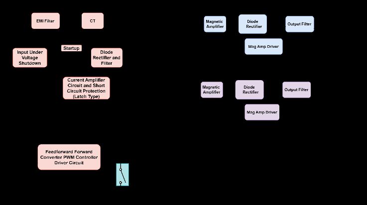
Fig.3Blockdiagramofthesystem
Bias winding is employed to produce the bias voltage required to energize the controller circuits. This voltage is maintainedatagreaterlevelthanthestart-upcircuitvoltage to ensure that a PWM controller circuit draws current from thebiaswindingratherthanthestart-upcircuit Thecurrent Transformer senses the Input current and protects the converterfromovercurrentandshortcircuitcurrent.Forthe controllingSwitchintheInputsideof theforwardConverter because of variation in Input power supply from 34V-44V Another name for a Mag-Amp is a saturable inductor. The typical Transformer and Inductor have ferrite-based high-
International Research Journal of Engineering and Technology (IRJET) e-ISSN: 2395-0056
Volume: 11 Issue: 08 | Aug 2024 www.irjet.net p-ISSN: 2395-0072
impedance cores, which must not reach saturation as their primaryfunctioninthecircuitisenergytransfer.Mag-Ampis employed in circuits as a switch. It should exhibit high impedance while not saturated and zero impedance when saturated,likeanidealswitch.
ThedesignspecificationsoftheproposedForwardConverter areshowninTable1.
Table1SpecificationoftheConverter
Minimuminputvoltage 28V
Maximuminputvoltage 44V
Outputvoltage(Vout1,Vout2) +8.2V,-8.2V
Outputcurrent(Iout1,Iout2) 5.7A,0.5A
Range –55°Cto125°C
4.1.TransformerCoreSelection
Theoptimumdesignisdecidedbythesmallsizeandlower dissipation of transformer, so Window Factor (Kw), Flux Density (Bm) & Current Density (J) values are assumed, for optimaldesigningbypreventinghazardousvoltagecontact
MagneticAmplifiercoreselectionusing
Selected core is P/N: 6-L2016-W763 (Nanocrystalline MagAmpCores)
4.2.SelectionofMOSFETswitch
The choice of MOSFET is contingent upon several factors, includingtheDrain-Sourcevoltage(VDS),Draincurrent(Id), Drain-Source ON resistance (Rds_on), Gate charge (Qg), and OutputCapacitance(Coss).Theselectionanddimensionsofa MOSFETaredeterminedbythelossesthatoccurwithinit.
IRHM57260, 200V, 0.049 Ohm, 32@ 100 Deg has been selected.
4.3.OutputFilter
The secondary output voltage of Transformers is rectified and filtered in order to achieve the desired output parameters.TheproposedconverterutilizesanLCfilter,and it is crucial to select the optimal values for this filter. This ensuresthattheconvertershaveminimalnoise,arecompact, and cost-effective, which are the primary requirements for Spaceapplications.
) ( )
4.4.SecondaryDiodeSelection
The selection of the output diode is contingent upon the magnitude of the secondary current and voltage. The essential requirement for these diodes is that they must operate at high frequencies. During the transition from the ON state to the OFF state, the reverse recovery time of a standard signal or p-n diode typically ranges in the order of hundredsofnanoseconds.However,forfastrecoverydiodes, thisperiod islessthan100 nanoseconds. Ontheother hand, Schottky diodes have an extremely low reverse recovery time,almostnil.Schottkydiodesareveryappropriatedueto their minimal forward voltage drop (VFD), high current capacity(IF),andlowreverserecoverytime(Trr)
Selecteddiodeis35CGQ100,100V,35A,TO-254AA,VFD:0.6.
Core selected is 0R43019UG, material, Ur:5010, AL: 6680mH/1000T
The converter is activated by a direct current (DC) voltage source and its output is linked to an electronic load that measures the output voltage and load current. A digital storage oscilloscope (DSO) is connected to measure the rippleintheoutputs.
International Research Journal of Engineering and Technology (IRJET) e-ISSN: 2395-0056
Volume: 11 Issue: 08 | Aug 2024 www.irjet.net p-ISSN: 2395-0072
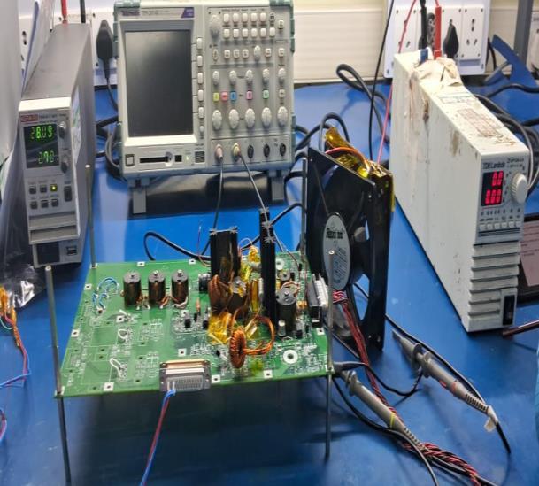
Fig.4.HardwareSetup
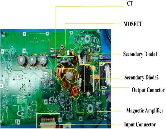
Fig.5.TopView
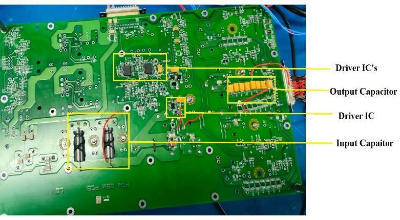
Fig.6.BottomView
Fig 5 The hardware setup includes a Hardware Board, a MultimeterformeasuringVoltageandcurrent,aDCSupplyfor providing input voltage to the converter, a CRO for measuring
and capturing the waveform, and an Electronic Load for measuringtheoutputvoltageandcurrent.
Hardware resultsfortheconverteratvarious loadcondition andinputvoltagearediscussedbelow.
6.1. MOSFET
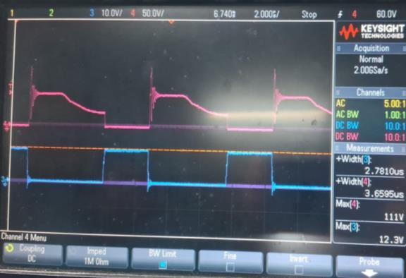
Fig.7.VgsandVdsat34V
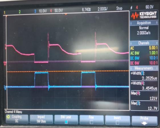
Fig.8.VgsandVdsat38V
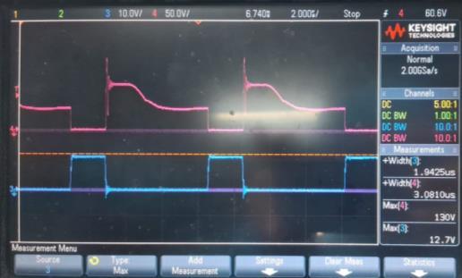
Fig.9.VgsandVdsat43V
International Research Journal of Engineering and Technology (IRJET) e-ISSN: 2395-0056
Volume: 11 Issue: 08 | Aug 2024 www.irjet.net p-ISSN: 2395-0072
TableshowstheMOSFTVgs,VdsandDutycycleReadingsfora VariousInputVoltage
Table2Vgs,VdsandDutyatvariousinputvoltage
6.2.Mag-AmpOutput
MAG-AMP Voltage Waveform output 1 at Full load condition. Fig 10, Fig 11 and Fig 12 shows Voltage across Mag-Amp at 34V, 38V and 43V input voltages respectively measuredatFullloadcurrent(5.7A)conditions.
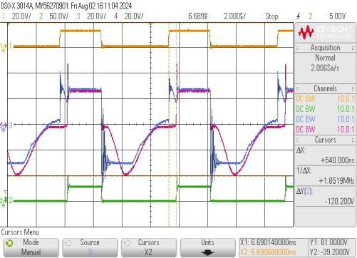
Fig.10.Mag-AmpOutput1at34V
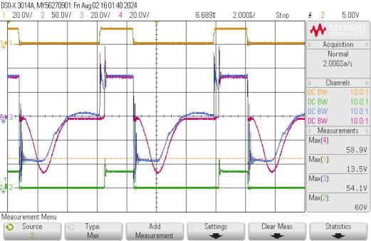
Fig.11.Mag-AmpOutput1at38V
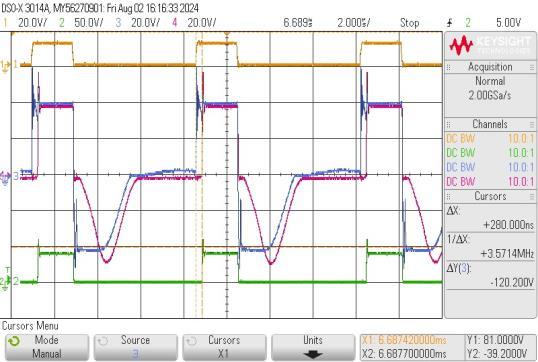
Fig.12.Mag-AmpOutput1at43V
TableshowstheMag-AmpBlockingtimeatvariousinputvoltage andloadcondition
Table3Mag-Ampblockingtime
6.3.EfficiencyatFullload
Table4showstheOutputtransformervoltage,DrainVoltage, Ripple voltage, Output Voltage, and Efficiency calculated at various Voltages. From the table, it is observed that at maximum Efficiency is achieved at 34V. The overall Efficiency of theconverteris>70%isachievedasthespecifiedvalue.
Table4Efficiencycalculationatvariousvoltage
International Research Journal of Engineering and Technology (IRJET) e-ISSN:
Volume: 11 Issue: 08 | Aug 2024 www.irjet.net
6.4.OutputRippleVoltage
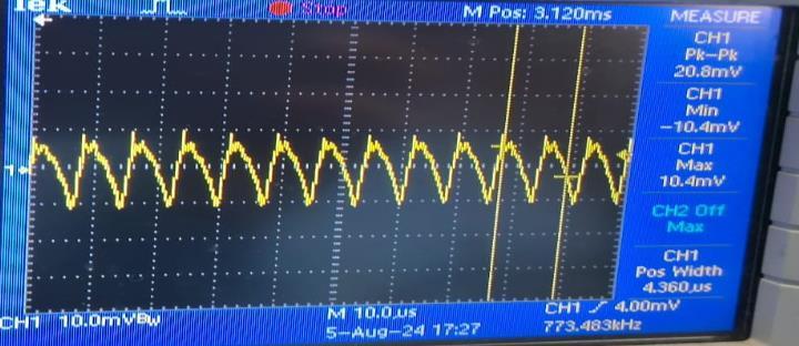
Fig.11.Output1rippleat38V
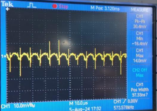
Fig.12.Output2rippleat38V
Table5showstheoutput1ripplevoltageatvariousvoltages
Table5Mag-Ampblockingtime
6.5.Lineand LoadRegulation
Table6showsthelineandloadregulationatvariousinput voltageandloadcondition
Table6Lineandloadregulation
7. CONCLUSION
Line and Load regulations met the required standards and were comfortably within 1% (0.44% and 0.06% respectively).
The output voltage exhibits a maximum change of 5% while the input voltage ranges from 34V to 44V. The converter's efficiency exceeds the specified value of 70% and is deemed satisfactoryaccordingtothespecifications.Hence,thePower Supply is specifically built to meet special needs and is wellsuitedforuseinSpaceapplications.
[1] X. Xiong, X. Ruan, H. Xi and J. Ge, "Feed-Forwarding the Output Voltage to Improve Efficiency for Envelope-Tracking Power Supply Based on a Switch-Linear Hybrid Scheme," in IEEE Transactions on Power Electronics, vol. 26, no. 8, pp. 2106-2111, Aug. 2011, doi: 10.1109/TPEL.2011.2119494.
[2] Suresh Kumar Tummala, Lenine Duraiswamy, “Switched Mode Power Supply: A High Efficient Low Noise Forward Converter Design Topology”, 2022 IEEE 2nd International Conference on Sustainable Energy and Future Electric Transportation (SeFeT), Hyderabad, India (2022), August 04-06. Doi: 10.1109/SeFeT55524.2022.9908809.
[3]NeshJ,BhoopendraKumarSinghet.al,“OverviewofSpaceGrade PowerSupplyModulesforSatellite”,EditedbyPSRSrinivasaSastry, Jiji CVet.al,Advancesin SmallSatellite Technologies,Lecture Notes in Mechanical Engineering. Springer, Singapore, May (2020), pp. 257-271.Doi:10.1007/978-981-15-1724-2_27.
[4] Gerry Moschopoulos, IEEE Press Editorial Board Sarah Spurgeon, Editor in Chief, “DC-DC Converter Topologies: Basic to Advanced”,Wiley-IEEEPress,NewJersey,(2024).
[4] Soumya K, Arpitha Raju B et.al, “Single Output 40W DC-DC Forward Converter for Space Application”, International Research Journal of Engineering and Technology, vol. 09, Issue.05, May (2022),pp.3165-3173.
[5] Guthi Prakash, Santosh B L and Bhoopendra Kumar Singh, “SpaceborneforwardconverterwithdiscreteLDOtopowerOCXO”, 2020 International Conference on Smart Technologies in Computing, Electrical and Electronics (ICSTCEE), Bengaluru, India (2020), December 09-10, Doi: 10.1109/ICSTCEE49637.2020.9276812.
[6] A. Bhat, K. U. Rao, Praveen P K, B. K. Singh and V. Chippalkatti, "Multiple output forward DC-DC converter with Mag-amp post regulators and voltage feedforward control for space application", 2016 Biennial International Conference on Power and Energy Systems: Towards Sustainable Energy (PESTSE), (2016), pp. 1-6, doi:10.1109/PESTSE.2016.7516488.
International Research Journal of Engineering and Technology (IRJET) e-ISSN: 2395-0056
Volume: 11 Issue: 08 | Aug 2024 www.irjet.net p-ISSN: 2395-0072
[7] Abraham I, Pressman et.al, Wendy Rinaldi- Sponsoring Editor, “Switching power supply design”, Third Edition, McGraw-Hill Publication,NewYork,(2009).
[8] Xu Congwen, Ma Qishuang et.al, “Closed-Loop Gate Drive for Single-Ended Forward Converter to Reduce Conducted EMI”, IEEE Access, Vol. 8, June (2020), PP (99):1-1, Doi: 10.1109/ACCESS.2020.3005239
[9] Soumya Patil, R.S. Geetha et.al, “Design and implementation of multiple output forward converter with Mag-Amp and LDO as post regulators for space application”, International Journal of Engineering Science and Technology, vol. 12, Issue.03, May (2020), pp.43-56.,DOI:10.4314/ijest.v12i3.5.
[10] Hesamodin Allahyari, Mohammad Ali Latifzadeh et.al, “An Improved Single Switch Wide Range ZVS Forward Converter Controlled with Variable Magnetizing Inductance”, IEEE Journal of Emerging and Selected Topics in Industrial Electronics, vol. 5, Issue.3, July (2024), pp. 837- 847. Doi:10.1109/JESTIE.2023.3311170.
[11] Jennifer Ian G. Ligtao, Chinet M. et.al, “Implementation of OnchipOVP,OCPandOTPCircuitsforDC-DCConverterDesign”,2018 IEEE10thInternationalConference onHumanoid,Nanotechnology, Information Technology,Communication and Control,Environment and Management (HNICEM), Baguio City, Philippines (2018), November29-December02.Doi:10.1109/HNICEM.2018.8666254.
[12]S.Kuruva,C.G.Satyaraddiet.al,"DesignandImplementationof Multiple Output DC-DC Converter with Output Power Sequencing", 2021 6th International Conference for Convergence in Technology (I2CT), Maharashtra, India (2021), April 02-04, Doi: 10.1109/I2CT51068.2021.9417822. © 2024, IRJET | Impact Factor value: 8.315 |