
International Research Journal of Engineering and Technology (IRJET) e-ISSN: 2395-0056
Volume: 11 Issue: 08 | Aug 2024 www.irjet.net p-ISSN: 2395-0072
International Research Journal of Engineering and Technology (IRJET) e-ISSN: 2395-0056
Volume: 11 Issue: 08 | Aug 2024 www.irjet.net p-ISSN: 2395-0072
Rajashekar D S1 , Vasundhara Patel K S2
1Dept. of ECE, BMS College of Engineering, Bengaluru, India
2Professor, Dept. of ECE, BMS College of Engineering, Bengaluru, India
Abstract - As deep sub-micron systems evolve and incorporate more advanced technologies, such as shrinking transistor sizes and increasing memory densities, the memory arrangement and testing strategies for any post silicon faults can become increasingly complex. Conventional testing using ATE (Automatic Test Equipment) consumes more test time and test cost, so an automated test strategy for such designs is needed. Automated testing strategies like Memory BIST involves incorporatingspecializedcircuitrywithinthememory itself to facilitate self-testing of the memory. This can significantly reduce the need for external test equipment and streamline the testing process while also minimizing the overall testing costs. Taking advantage of the same, Memory BIST architecture is implemented in this project work. The introduction of BIST circuitry on a chip can indeed bring advantages like reduced testing costs and self-testing capabilities, but it also leads to increased power consumption due to the additional logic andincreasedswitchingactivity. To mitigate this issue and maintain low power dissipation, Implementation of a Clock gating technique is done in this project. Clock gating insertion has been done during the synthesis stage in Cadence Genus tool. Memory BIST insertion is carried out in Tessent MBIST Architect and the Power analysis is done in Cadence Genus Joules. Simulation results and Power analysis results proves that the MBIST insertion is done without any mis compares. Also the difference in power consumption before and after the insertion of ICG (Integrated Clock Gating) cells is observed.
Key Words: MBIST; MARCH Algorithm; ICG; Tessent MBISTArchitecttool; CadenceGenusJoulestool
Today's cutting-edge semiconductor industry is characterizedbyarapidpaceofSoCdevelopment.Theneed for embedded memories keeps growing since more and more functions are added to the die. Sub-micron devices have many memories that call for smaller footprints and quickeraccesstimes.Itbecomesveryimportanttotestthese memoriesforpost-silicondefects.
BIST offers several advantages over traditional external testingmethodsthatrelyonspecializedequipmentortest vectors. By enabling circuits to test themselves without externalintervention,BISTreducestheneedforexpensive andcomplextestequipmentandinterfaces.Thissimplifies thetestingprocesswhileincreasingtestcoverage,ascircuits
cangenerateandapplytailoredtestpatterns.Furthermore, BIST facilitates faster and more reliable testing by performingself-checksandself-repairsduringoperationor atpredefinedintervals.Thedifficultiesandconstraintsthat come with using BIST techniques in CMOS circuit design mustbetakenintoconsideration.BISTraisestheoverhead andcomplexityofthecircuit,whichmayhaveanimpacton thecost,area,power,andspeed.
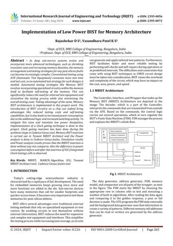
TheController,Interface,andWrapperthatmakeupthe Memory BIST (MBIST) Architecture are depicted in the image. The decoder, which is a part of the Controller, interpretsthecommandsthataretransmittedfromoutside via the ATE. Based on the commands, the control logic carries out several operations, which in turn regulate the BIST'sFiniteStateMachine(FSM).FSMmanagestheprocess andexplainstheMBIST'swholeflow.
The data generator, address generator, FSM, memory model,andcomparatorareallpartsofthewrapper,asseen in the figure. The FSM starts the MBIST by choosing the appropriate row or column cells to test and executing a numberofbuilt-inalgorithms.Afterreadingthedataagain and comparing it to the golden response, a pass or fail decisionismade.TheATEprogramstheFSMstateexternally andthebackgrounddatageneratorusesthatinformationto createavarietyofpatterns.Differentmemorycelladdresses that can be read or written are generated by the address generator.
International Research Journal of Engineering and Technology (IRJET) e-ISSN: 2395-0056
Volume: 11 Issue: 08 | Aug 2024 www.irjet.net p-ISSN: 2395-0072
Memory arrays in integrated circuits are tested for integrityandoperationusingMBIST(MemoryBuilt-InSelfTest)methods.Inordertoidentifydefectsincludingstuck-at faults,transitionfaults,couplingfaults,retentionfaults,and others,thesealgorithmscarryoutavarietyofreadandwrite operations. The following are a few popular MBIST algorithmsandarebroadlyclassifiedintotwotypes,
A Classical Algorithms - They are subdivided into MSCANorZero-OneAlgorithm, CheckerboardAlgorithm, GallopingAlgorithm(GALPAT),ButterflyAlgorithm
B. March Algorithms - MATS Algorithm , MATS+ Algorithm,MATS++Algorithm MarchXAlgorithm,MarchC Algorithm,MarchC-Algorithm
MARCH C- Algorithm Implementation
TheMarchC-algorithmconsistsofasequenceofoperations (read and write) that are applied to each memory cell in ascendinganddescendingaddressorder.Theoperationsare designedtosystematicallytesteachcellforpotentialfaults. Here is the sequence of operations in the March Calgorithm:
{⇕(w0); ⇑(r0,w1); ⇑(r1,w0); ⇓(r0,w1); ⇓(r1,w0);⇕ (r0)}
StepsoftheMarchC-Algorithm
Step 1: Write0toallcells⇕(w0)i.e,Initialiseallcellsto0 bothinascendinganddescendingorder
Step 2: Read0,Write1{⇑(r0,w1)} Foreachcell,readthe valueandensureitis0,thenwrite1tothecell.Thisstepis performedinascendingaddressorder.
Step 3: Read1,Write0{⇑(r1,w0)} Foreachcell,readthe valueandensureitis1,thenwrite0tothecell.Thisstepis performedinascendingaddressorder.
Step 4: Read0,Write1{⇓(r0,w1)} Foreachcell,readthe valueandensureitis0,thenwrite1tothecell.Thisstepis performedindescendingaddressorder.
Step 5: Read1,Write0{⇓(r1,w0)} Foreachcell,readthe valueandensureitis1,thenwrite0tothecell.Thisstepis performedindescendingaddressorder.
Step 6: Read0fromall cells ⇕ (r0)i.e,read0 fromall the cells and ensure it is 0 both in ascending and descending order.
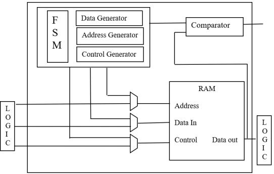
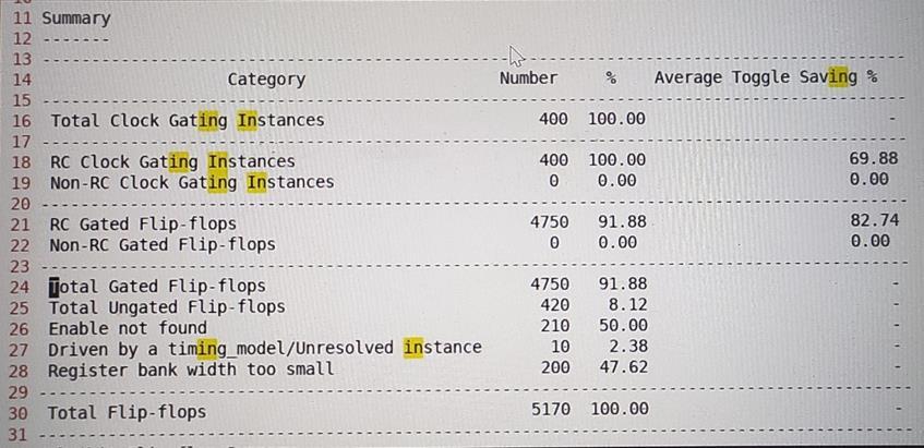
The implemented methodology shown above broadly consistingoffourpartswhichareMBISTinsertion,Power analysis before Clock gating, Clock Gating insertion and PoweranalysisafterClockGating.
Thebriefflowoftheprojectisexplainedasfollows,RTL code has been fed to the tool(Tessent MBIST Architect) which inserts the MBIST logic to the design. Then we performSynthesisontheMBISTinsertedRTLthatconverts RTLcodetoGatelevelNetlist.Thisnetlisthasbeenfedtothe tool(CadenceJoules)whichinsertsICGcellstothedesignthat enablestolowerthedynamicpowerdissipation.Henceable to test and detect the memory faults with reduced power dissipation.The detailed MBISTflowandClock gatingthat hasbeenimplementedisdiscussedinthefurthersections.
Implementation of MBIST Flow
International Research Journal of Engineering and Technology (IRJET) e-ISSN: 2395-0056
Volume: 11 Issue: 08 | Aug 2024 www.irjet.net p-ISSN: 2395-0072
Step 1
RTLdesignisbeingloadedtothetoolalongwiththe necessarylibraries.
SpecifyingMBISTrequirementsinvolvesthedetails aboutdesigninformation,memoryinformationand DFTrequirements.
Design information such as number of clocks, frequencyofclocks,UPF(Unitypowerfactor)files. Memoryinformationsuchasnumberofmemories, typeofmemories,numberofports,testalgorithmto beused.DFTrequirementssuchasMaxpowerper step,Maxtesttimeperstep,Maxmemoriesperstep.
Once the design is loaded and specifying the requirements, we run the Design Rule Checking(DRC) to detect if any design issues are present
Step 2 : CreateandProcessDFTSpecifications
ThisstepinvolvesgenerationofDFTSpecifications that are necessary for MBIST insertion. Also ModificationofDFTSpecificationisalsodoneasper therequirementduringthisstep.
Once the proper DFT Specifications are defined, thenit’llgenerateandinserttheMBISThardware intotheRTLdesignasperthespecifications.
Step 3: ICL
The main goal of ICL Extraction is automated generation of the interconnection information of variousIJTAGbuildingblocks(Instruments,SIBs, TDR’s).
ICL extraction process verifies the proper connectivityoftheICLmodulesthatwereinserted with the process_dft_specification. ICL extraction mustpasswith no violationsinorder togenerate testpatterns.
Step
Pattern specification defines a series of pattern wrappersforagivenviewofadesign
Step
AftercreatingandprocessingPatternspecification, thefinalstepintheMBISTimplementationflowis the Simulation validation. Here we run the simulationusingMemoryBISTverificationpatterns and then check the test bench simulations using Tessentshellenvironment.
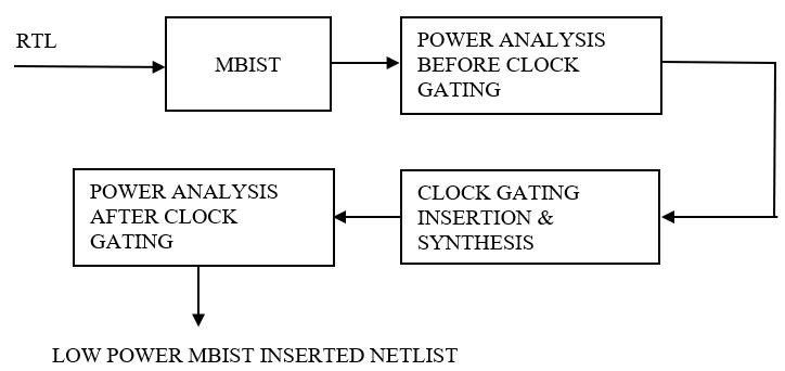
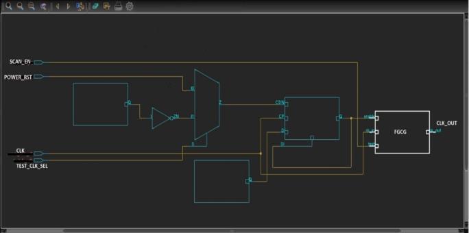
Clock gating technique involves the insertion of ICG (Integrated Clock Gating) cells into the design. When designingdigital circuits,anIntegratedClock Gating(ICG) cellisessential,especiallyforpowercontrol.Bycuttingoff the clock signal to certain circuitry while it's not in use, a techniqueknownasclockgatinghelpssynchronousdigital systemsconsumelessdynamicpower.TheICGcellisbuiltto carry out this method efficiently. The typical ICG cell isas shownbelow.
Operation of ICG
The ICG cell works by taking an enable signal and the original clock signal as inputs. When the enable signal is active, the clock signal is allowed to pass through to the gatedclockoutput.Whentheenablesignalisinactive,the clocksignalisblocked,effectivelydisablingtheclockingof thedownstreamcircuitry.
WhenEN=1,GCLK=CLK(theclocksignalispassed through)
WhenEN=0,GCLK=0(theclocksignalisblocked)
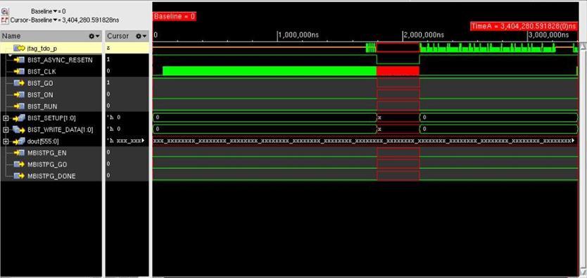
MBIST Insertion & Validation
BIST_CLK -ItcontrolstheentireBISToperationasitdrives theblockthatcontainsmemories.IfBIST_CLKisnotpulsing properly,thentheMBISTinsertionandValidationfails.
MBIST_EN -Thispin/signaldescribeswhethertoperform MBIST insertion or not. i.e, Tool will be able to perform MBISTonlyifMBIST_ENissetHIGH.
MBIST_GO - This signal will be flagged if any errors occurred or not during the execution of MBIST algorithm. MBIST_GO will be HIGH at start of the test. If any error, MBIST_GOtransitionstoLOW.
MBIST_DONE – This signal will be flagged whether the algorithm execution has been completed or not. MBIST_DONEwillbeLOWwhiletestruns,goesHIGHwhen testiscompleted,returnsLOWaftercontroller resultsare extracted.
International Research Journal of Engineering and Technology (IRJET) e-ISSN: 2395-0056
Volume: 11 Issue: 08 | Aug 2024 www.irjet.net p-ISSN: 2395-0072
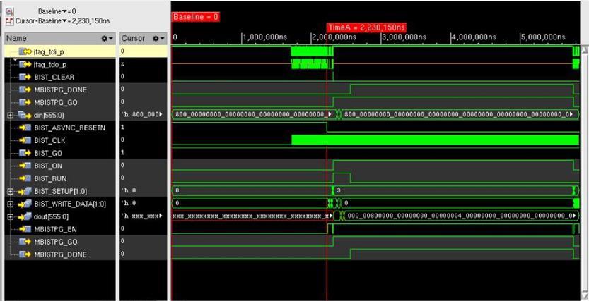
CheckingGOandDONEsignals,
DONEhigh+GOhighmeanstestrantocompletionwithout errors
DONE low + GO high means test not yet complete and no errorsyet
DONE high + GO low means test ran to completion with errors
DONElow+GOlowmeanstestnotyetcompleteanderror alreadyencountered
International Research Journal of Engineering and Technology (IRJET) e-ISSN: 2395-0056
Volume: 11 Issue: 08 | Aug 2024 www.irjet.net p-ISSN: 2395-0072
Power consumption before ICG cell insertion
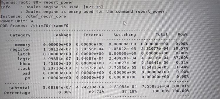
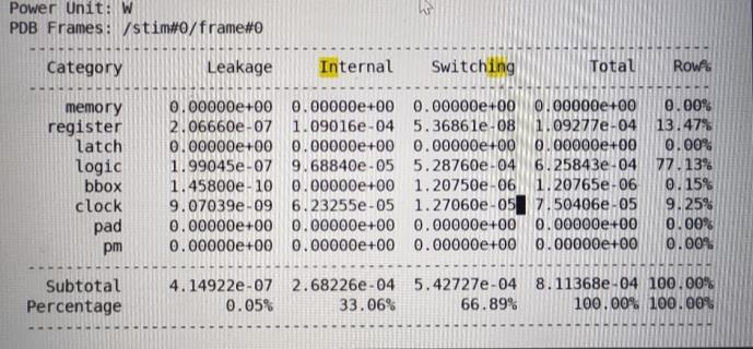
Fig 12. PowerreportafterICGcell
UnlikethepowerreportofthedesignbeforeICGinsertion, whichhasconsumed8113680000nW Itisclearlyevident thatthepowerdissipationaftertheinsertionofICGcellshas beenreducedandconsumedonly7558310000nW,which meansthepowerdissipationhasbeenreducedby7%.The power report is shown above and also the power values obtainedhasbeentabulatedasshownbelow.
Table 1. PowermeasurementsofMBISTinsertednetlist beforeandafterClockGating
Totalpower consumptionbefore clockgating (W)
Totalpower consumptionafter clockgating (W) MBISTinserted Netlist 8.11368E-04 7.55831E-06
The work that has been carried out as a part of this project is majorly on the MBIST Insertion for memory architecturetoenabletheintegratedcircuitsforself-testing on its own and Clock Gating insertion for reduced power consumption.
The implementation has been carried out at RTL level and the design is being synthesized to get the gate level netlistforpoweranalysis.Firstly,MBISTinsertionisdone and power report is generated for that design and the readingsarenotedwithoutinsertionofICGcells.Then,the same MBIST flow is repeated again and power report is generatedaftertheinsertionofICGcells.Itwasclearfrom theobtainedresultsthatthepowerconsumptionhasbeen reducedsignificantly.
Whiletestinganddetectingmemorymoduleerrorswas achievable in this work, but the errors were not repaired. Additionally,thereispotentialtousecuttingedgelowpower implementationapproachestofurtherminimizethepower usage.
Inthefuture,
ItispossibletoaddmoreBISR(BuiltinSelfRepair) hardwaretothefunctionallogictoenableboththe detectionandcorrectionofdefects.
There is a scope to use advanced low power approacheslikeFSMpartitioning,Multilevelvoltage scaling,andSupplyvoltagescaling.
[1] A.Manzone,P.Bernardi,M.Grosso,M.Rebaudengo, E.SanchezandM.S.Reorda,"IntegratingBISTtechniquesfor on-lineSoCtesting,"11thIEEEInternationalOn-LineTesting Symposium,FrenchRiviera,France,2005,pp.235-240,doi: 10.1109/IOLTS.2005.38.
[2] S.B.GhaleandN.P,"DesignandImplementationof Memory BIST for Hybrid Cache Architecture," 2021 6th InternationalConferenceonCommunicationandElectronics Systems (ICCES), Coimbatre, India, 2021, pp. 26-31, doi: 10.1109/ICCES51350.2021.9489225.
[3] T.Q.Bui,L.D.Pham,H.M.Nguyen,V.T.Nguyen,T. C. Le and T. Hoang, "An Effective Architecture of Memory Built-In Self-Test for Wide Range of SRAM," 2016 International Conference on Advanced Computing and Applications(ACOMP),CanTho,Vietnam,2016,pp.121-124, doi:10.1109/ACOMP.2016.026.
[4] S. S. Rao Dannina and U. V. Ratna Kumari, "Error TolerantMBISTDesignwithEfficientHighThroughputand Low Power Reversible Techniques," 2021 10th IEEE International Conference on Communication Systems and NetworkTechnologies(CSNT),Bhopal,India,2021,pp.230235,doi:10.1109/CSNT51715.2021.9509611.
[5] A.S.Abu-Issa,"Energy-EfficientSchemeforMultiple Scan-Chains BIST Using Weight-Based Segmentation," in IEEETransactionsonCircuitsandSystemsII:ExpressBriefs, vol. 65, no. 3, pp. 361-365, March 2018, doi: 10.1109/TCSII.2016.2617160.
[6] M.MosalgiandG.Hegde,"PowerOptimizedTPGfor BISTArchitecture,"2017IEEEInternationalConferenceon ComputationalIntelligenceandComputingResearch(ICCIC), Coimbatore, India, 2017, pp. 1-4, doi: 10.1109/ICCIC.2017.8524577.
[7] P.Liu,J.Wu,Z.You,M.Elimu,W.WangandS.Cai, "DefectAnalysisandParallelMarchTestAlgorithmfor3D Hybrid CMOS-Memristor Memory," 2018 IEEE 27th Asian Test Symposium(ATS),Hefei,China,2018,pp.25-29, doi: 10.1109/ATS.2018.00016.
[8] A.KincelandM.Balaz,"MBISTforLEON3processor core cache," 2013 IEEE 16th International Symposium on
International Research Journal of Engineering and Technology (IRJET) e-ISSN: 2395-0056
Volume: 11 Issue: 08 | Aug 2024 www.irjet.net p-ISSN: 2395-0072
Design and Diagnostics of Electronic Circuits & Systems (DDECS),KarlovyVary,CzechRepublic,2013,pp.287-288, doi:10.1109/DDECS.2013.6549836.
[9] A.S.Abu-IssaandS.F.Quigley,"Bit-SwappingLFSR andScan-ChainOrdering:ANovelTechniqueforPeak-and Average-Power Reduction in Scan-Based BIST," in IEEE Transactions on Computer-Aided Design of Integrated CircuitsandSystems,vol.28,no.5,pp.755-759,May2009, doi:10.1109/TCAD.2009.2015736.
[10] W. Kang, C. Lee, H. Lim and S. Kang, "Optimized Built-In Self-Repair for Multiple Memories," in IEEE TransactionsonVeryLargeScaleIntegration(VLSI)Systems, vol. 24, no. 6, pp. 2174-2183, June 2016, doi: 10.1109/TVLSI.2015.2499387.
[11] Y. J. M. Shirur, H. R. Lakshmi and V. S. Chakravarthi, "ImplementationofAreaEfficientHybridMBISTforMemory Clusters in Asynchronous SoC," 2014 Fifth International SymposiumonElectronicSystemDesign,Surathkal,India, 2014,pp.226-227,doi:10.1109/ISED.2014.57.
[12] T. Tewary and A. Sen, "A novel approach to realize built-in-self-test(BIST) enabled UART using VHDL," 2014 First International Conference on Automation, Control, EnergyandSystems(ACES),Adisaptagram,India,2014,pp. 1-6,doi:10.1109/ACES.2014.6808031.
[13] Dong Xiang, Ming-Jing Chen, Jia-Guang Sun and Fujiwara,"Improvingtestqualityofscan-basedBISTbyscan chain partitioning," 2003 Test Symposium, Xi'an, China, 2003,pp.12-17,doi:10.1109/ATS.2003.1250773.
[14]K.Lee,S.Lee,J.Park,I.LeeandS.Kang,"ALow-Power BIST Scheme Using Weight-Aware Scan Grouping and Scheduling for Automotive ICs," in IEEE Access, vol. 9, pp. 116115-116132,2021,doi:10.1109/ACCESS.2021.3105429.
[15]S.R.Chand,V.Srinivas,T.V.Sai,M.SailajaandT.Madhu, "Fault diagnosis for using TPG low power dissipation and highfaultcoverage,"2010IEEEInternationalConferenceon Computational Intelligence and Computing Research, Coimbatore, India, 2010, pp. 1-5, doi: 10.1109/ICCIC.2010.5705884.
[16]J.WibbenmeyerandC.-I.H.Chen,"Built-InSelf-Testfor Low-Voltage High-Speed Analog-to-Digital Converters," in IEEE Transactions on Instrumentation and Measurement, vol. 56, no. 6, pp. 2748-2756, Dec. 2007, doi: 10.1109/TIM.2007.908343.
[17] D. Xiang, X. Wen and L. -T. Wang, "Low-Power ScanBasedBuilt-InSelf-TestBasedonWeightedPseudorandom Test Pattern Generation and Reseeding," in IEEE TransactionsonVeryLargeScaleIntegration(VLSI)Systems,
2024, IRJET | Impact Factor value: 8.226 |
vol. 25, no. 3, pp. 942-953, March 2017, doi: 10.1109/TVLSI.2016.2606248.
[18]D.Ghosh,S.BhuniaandK.Roy,"Atechniquetoreduce powerandtestapplicationtimeinBIST,"Proceedings.10th IEEE International On-Line Testing Symposium, Funchal, Portugal, 2004, pp. 182-183, doi: 10.1109/OLT.2004.1319684.
[19]V.Thirunavukkarasu,R.SaravananandV.Saminadan, "Performance of low power BIST architecture for UART," 2016InternationalConferenceonCommunicationandSignal Processing(ICCSP),Melmaruvathur,India,2016,pp.22902293,doi:10.1109/ICCSP.2016.7754103.
[20]C.Zoellin,H.-j.Wunderlich,N.MaedingandJ.Leenstra, "BISTPowerReductionUsingScan-ChainDisableintheCell Processor,"2006IEEEInternationalTestConference,Santa Clara, CA, USA, 2006, pp. 1-8, doi: 10.1109/TEST.2006.297695.