
International Research Journal of Engineering and Technology (IRJET) e-ISSN: 2395-0056
Volume: 11 Issue: 08 | Aug 2024 www.irjet.net p-ISSN: 2395-0072

International Research Journal of Engineering and Technology (IRJET) e-ISSN: 2395-0056
Volume: 11 Issue: 08 | Aug 2024 www.irjet.net p-ISSN: 2395-0072
Ashish Kumar N H1, Dr. Anitha G S2, Santosh B L3, Bhoopendra Kumar Singh4, Suriya S5
1Dept of Electrical and Electronics, RV College of Engineering, Bengaluru, India
2Dept of Electrical and Electronics, RV College of Engineering, Bengaluru, India
3Assistant manager, Design, Centum Electronics Ltd, Bangalore, India
4Director, Design, Centum Electronics Ltd, Bangalore, India
5Engineer, Design, Centum Electronics Ltd, Bangalore, India
Abstract- The power supply module in the space application use Forward Converter topology due to its advantage such as reduction in weight and providing the isolation on input & output of the converter. The Forward Converter having the high switching frequency of 140KHz to reduce the size of the converter with the feed forward technique and PWM controllerUC2525IC. MOSFET is used for the switching and RCD snubber are used to decrease the stress of MOSFET. The driver IC used to control the gate pulse of MOSFET and LM358 IC are used. The proposed converter is of 5V/2A single output for the input range of 30V-44V. Output of the converter is controlled by Mag-amp connected across the secondary winding of the transformer with some output filters. The paper describes about design, analysis, hardware implementation of efficient DC DC converter with Forward converter for low power application. The converter requires some major protection such as under voltage protection, over voltage protection, over current protection and short circuit protection. The proposed converter provides the lesser output ripple and better efficiency at the nominal voltage along with full load condition. The hardware of this converter is tested for the various input voltage and different load condition with nearlyconstantoutputvoltage
Keywords Forward converter, PWM controller, Mag amp, Protection Circuit, Filters
Switched-mode power converters are now extensively utilized because they are smaller and more efficientthanconventionalpowersources.Reducedsizeand weight are the advantages of SMPS which is required for space applications. The present space research organizations drive towards lighter, smaller, more efficient, low-cost and high-reliable power supply[1]. Satellites employ a variety of dc/dc converters in their electrical power systems. The heritage design features of the dc/dc convertertopologiesutilizedinsatellitesdifferfromthoseof the dc/dc converters used on Earth[2].The most popular
topologies for isolated output voltage and low power applications are forward converter due to their tiny transformer size, simple structure, and efficiency[3].With theseconverters,transformerdemagnetizationisapotential risk. Different transformer resetting strategies, such as (i) addinganadditionalresetwindingor(ii)utilizingasnubber circuit,canbeusedtodemagnetizetransformers[4].
The use of magnetic amplifiers, or "Mag-amps," is an easy andaffordablewaytomanageauxiliaryoutputs.Asaturable inductorusedforacontrolledswitchiscalledamag-amp[5]. Unsaturated coils have a high impedance and block the entire voltage, while saturated coils have zero voltage and carry the full current. Mag-amps provide several benefits, including low noise, excellent precision, power savings, and dependability[6][7]. An interesting approach to enable output voltage regulation at constant frequency is to increase the energy stored by the inductor and follow a conventional PWM control strategy[8].The most crucial components of the power supply unit are the protection circuits.Inadditiontoinputunder-voltageandoutputovervoltage protection, the proposed converter also includes output over current protection. The protective circuit activates when the output current surpasses 125% of the intended output current, shutting down the converter and preventingaseriousfailureofthepowersupplyunit[9].The core saturation theory underlies the operation of the Magamps.Thesearesaturableinductor,meaningthattheentire voltageappearsacrossthe mag-ampcoil,dropstozero,and carries the entire current when the core hits the saturation level. The coil blocks the entire voltage and no current passes through it when unsaturated[10][11]. Magnetic amplifiers work incredibly well and are simple to utilize as post regulators to control the secondary side's output voltage[12].Aresistor,capacitor,anddiode(RCD)clampcan be used as an alternate technique for resetting a forward convertertransformer.Theresistor,capacitor,anddiodeare theonlythreepartsofthestraightforwardRCDclampcircuit, which only needs a more straightforward two winding transformer. The clamp absorbs the magnetizing inductor energy as well as provides a discharge path for the leakage
International Research Journal of Engineering and Technology (IRJET) e-ISSN: 2395-0056
Volume: 11 Issue: 08 | Aug 2024 www.irjet.net p-ISSN: 2395-0072
inductance[13][14].Therefore, compared to the resetwinding approach, RCDclamp completely resets the transformerandgreatlyreducesvoltagestressonthepower switch. These factors make RCD clamp forward converters popularinthepowersupplysector[15].
Inputvoltage 30V–44DC
Topology ForwardDC-DC IsolatedConverter
Switchingfrequency 140kHz
Timeperiod 7.14uSec
Outputvoltage¤t 5V/2A
Lineregulation <1%
OutputVoltageRipple <50mV
Dutycycle
OutputPower
27%-40%
10W
OperatingTemperature Range –55°Cto125°C
Efficiency >70%
The converters required details are given in the table2.1.Asmentionedinthetable theinputvoltagevaries from 30V to 44V DC supply with the constant output of 5 Voltsand2Amps for the range ofinput.Forwardconverter topology is used with the converter having the switching frequencyof 140KHz.
TheconvertershouldhavetheLineregulationandtheLoad regulationlessthan1%oftheconverter.
The efficiency of the converter should be atleast of 70% or more than 70% which can be done by minimizing various loss.Theoutputvoltageshouldbemaintainedofconstant5 volts with the voltage ripple of less than 50m Volts for the variousloadcondition.
Other than all this specification the converter should have some protection circuit such as Under voltage protection, Overvoltage protection , Short circuit protection & Over currentprotectionforthebetteroperationtheconverter.
Alltheabovespecificationanddetailsareusedfordesigning oftherequiredconverter.
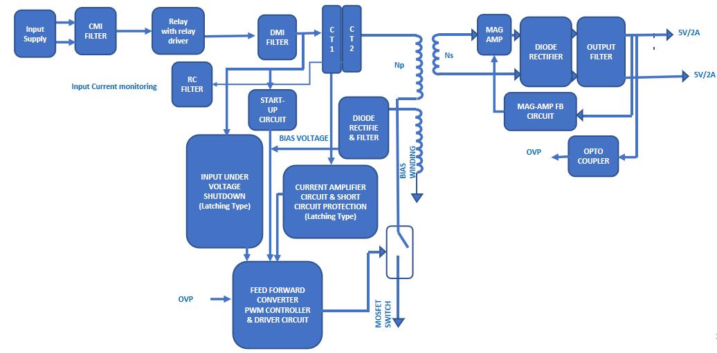
DiagramoftheForwardconverter
TheAbovefigureshowthecompleteblockdiagramofthe forward converter topology with all the essential components such as cmi filter, dmi filter, current transformer ,under voltageprotection ,startup circuit,short circuit protection, diode rectifier and filters, mag-amp, opto coupler,outputfilteretc.
Principle Of Operation Of Designed Forward Converter
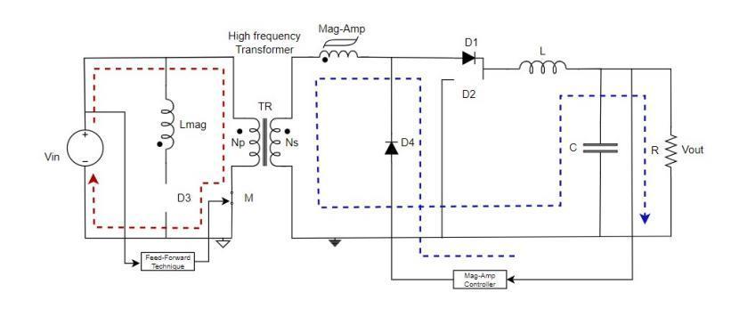
A forward converter is a kind of power converter that usesatransformertoprovideelectricalisolationbetweenthe input and output and to transition a direct current (DC) voltage from one level to a lower level. To put it simply, it safely transforms a greater voltage to a lower voltage and makes sure that the electrical components on the input and outputsidesarekeptapart,whichisessentialforbothsafety and noise reduction. The proposed converter consists of a Forward Converter controlled by voltage feed forward techniquewithMag-AmpaspostregulatorasshowninFig2.
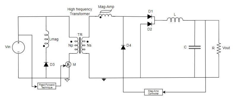
Fig.2:CircuitdiagramofForwardConverterwithvoltage feed-forwardtechniqueandmag-ampcontroller.
As shown in the above Figure, Vin is input supply to the Converterwhosevoltagevariesinrange(30Vto44V).TRis High frequency Transformer of the Converter for Isolation purpose. Lmag is the reset or demagnetizing winding of
International Research Journal of Engineering and Technology (IRJET) e-ISSN: 2395-0056
Volume: 11 Issue: 08 | Aug 2024 www.irjet.net p-ISSN: 2395-0072
Transformer. D3 is a reset winding Diode. M is the Mosfet, controlling switch of the converter. Mag-Amp is on the secondary side which is usually represented as Inductor withasmallBH-curvesymbolontopasshownintheabove diagram. It is connected in series with Secondary winding followingtheOutputrectifyingdiodeD1andD2.LandCare OutputFilters.RistheloadthenthevoltageacrossRisVout (Output Voltage) and then the current flowing is lout (Output Current). Output is regulated by Mag-Amp ControllerFeedback.D4istoblockthecurrentfromflowing intomag-ampcontroller.
Theoperationoftheproposedconvertercanbeexplainedin 4 modes, then the related circuit diagram and waveform is givenbelow:
MODE 1:
Inthismode,ConverterSwitchMisturnedON,and theinputvoltagehasbeenappliedtotheprimarywindingof the transformer. Current starts flowing on the primary side of Transformer, This generates a magnetic field in the transformer’s core, storing energy. Simultaneously, the voltage induced in the secondary winding and then the currentstartsbuildsupslowlyonsecondarysideduetothe samepolarities.D3isreversebiasedsonocurrentwillflow through Lmag winding. Due to the current on Secondary, Mag-amp slowly starts saturating and it blocks the current toflowthroughit.EntireSecondarysidevoltageisappeared acrossmag-ampandthennooutputvoltage.Thisiscalledas Blocking state. Corresponding Circuit diagram with current flowisshowninFig.3(a).
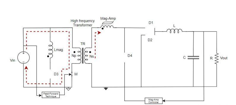
(a):CircuitdiagramofMode1operation(Blocking State).
MODE 2:
Inthismode,MisonconductionMode,mag-ampis fully saturated acts as a short circuit/ switch when closed. CurrentstartsflowinginDiodeD1,whichisforwardbiased. The secondary voltage is rectified by diode D1 and filtered by LC filters then appeared across the load R. This is called
as Conducting state. Corresponding Circuit diagram with currentflowisshowninFig.3(b).
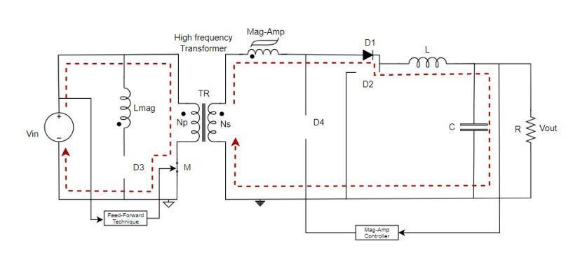
Fig.3(b):CircuitdiagramofMode2operation(Conducting State).
MODE 3:
In this mode, M is on conduction Mode, Output reachedtherequiredvalue.Whenoutputvoltagegoesmore than desired value the mag controller regulates output voltagetotheappropriatevaluebydesaturatingthecoreof mag-amp, thereby blocking the voltage of secondary. Now DiodeD4becomesforwardbiasedandallowsthecurrentto flow through it. This we can call it as controlling state. Corresponding Circuit diagram with current flow is shown inFig.3(c).
(c):CircuitdiagramofMode3operation(Controlling State).
MODE 4:
Inthismode,Misturned OFF,themagneticfieldin the transformer starts to collapse, and voltage across the primary winding reverses polarity. The diode connected in series with the primary winding i.e D3 (often taken as “freewheeling diode”) becomes forward-biased, providing a path for the magnetizing current to flow, thus resetting the transformer’s core. On the secondary side, the output diode D1 becomes reverse-biased. Diode D2 is Forward Biased providingapathforcurrenttoflowandtheenergyisstored in the output inductor L continues to supply the load through the output capacitor C. This we can call it as resetting state. Corresponding Circuit diagram with current flowisshowninFig.3(d).
International Research Journal of Engineering and Technology (IRJET) e-ISSN: 2395-0056
Volume: 11 Issue: 08 | Aug 2024 www.irjet.net p-ISSN: 2395-0072
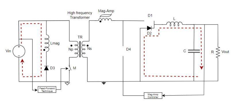
Fig.3(d):CircuitdiagramofMode4operation(Resetting State).
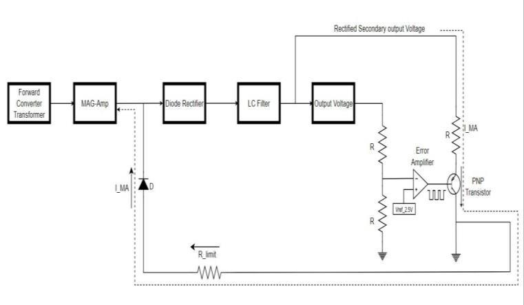
Working of Magnetic Amplifier:
MagneticAmplifierinshortcalledas Mag-Amp.Itis notexactlyamplifyinganygainasthenamesuggestsbutthe magneticpropertyofthecoreisusedtoregulatethevoltage aspertherequirement.Mag-AmpisalsoknownasSaturable Inductor. In the normal Transformer and Inductor ferrite based high impedance cores are used and they shouldn’t saturate, because the necessity of these in circuit is energy transfer.Whenitcomestomag-amptheyareusedincircuit asaswitch,theyshouldofferhighimpedancewhenitisunsaturated and then when saturated it should offer zero impedance/ resistance similar to an Ideal Switch. The working of Mag-Amp can be explained using the equivalent modelasshowninFig.e.
Fig.4:EquivalentmodelofworkingofMag-Amp. As shown in above Fig.4, the circuit has SPST switch (SW), mag-amp(MA),DCvoltagesupply(Vs),andLoadresistance (RL).Mag-Ampworkinglikeaprogrammablecontrolled
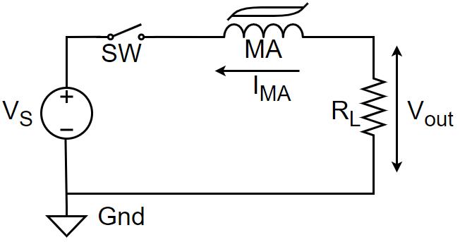
Fig.4:EquivalentmodelofworkingofMag-Amp.
switch. When the switch closes, it offers high relative permeabilityUr,andthushighimpedance.Duetoitsnature of not allowing any sudden change in current the voltage acrossMag-Ampisequaltoinputsupplyvoltage(Vs)andno current will be flowing through it. As the core is made of perm-alloy or Cobalt, the current in the core builds up rapidlywhichsaturatesthecoreandactsasaShortcircuitin turn providing a path for current to flow. The relative
permeability is shift from Ur to 1 and input voltage Vs will appear across load resistor RL. The interruption required because saturation of the MA coil is designed by opposite currentIMAappliedbythefeedbackloop.
Mag-Amp feedback controller will have a voltage feedbackfromOutputwhichisconnectedtoerroramplifier. Non-invertingpinofthisisconnectedtoreferencevoltageof 2.5Vandinvertingpinisconnectedtovoltage divider from output. When output voltage goes above the required value a negative error signal is generated which is amplified by erroramplifier.Thiserrorsignalisconnectedtobaseofthe PNP transistor which will be turning the transistor to conduction mode and a current starts flowing through it, thiscurrentislimitedbyRlimitresistor.NowtheDiodeDis Forward Biased and then a large current starts flowing through Mag-Amp in the reverse direction and desaturates the core thereby regulating the output voltage to appropriatevalue.TheMag-AmpControlCircuitisasshown inFig5.
Variations in input voltage affect the overall performance of the circuit through duty cycle variations. In order to avoid thatthere mustbe a loop which correctsthe dutycycle,sothateventhoughthereisachangeoftheinput voltage the output voltage is not affected. The voltage feed forward mode of PWM control is used which adjusts the dutyratioaccordingtothechangesintheinputvoltage.This typeoffeedforwardtechniqueusesRCnetworktogenerate saw tooth waveform using input voltage which is shown in the Fig 5(a) and also the expected waveform is shown Fig 5(b).
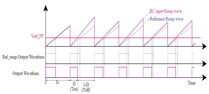
Fig.5 (a) & (b): Voltage Feed Forward Circuit and its waveform.
International Research Journal of Engineering and Technology (IRJET) e-ISSN: 2395-0056
Volume: 11 Issue: 08 | Aug 2024 www.irjet.net p-ISSN: 2395-0072
As the input goes high or doubles, the slope of the comparator will also doubles which causes the duty cycle will immediately be halved. This type of duty cycle correction is very much important for circuit in order to wait for an error amplifier to detect the error in the output voltage.
Design of Transformer,PWM Controller, MOSFET, Diode, Filter. Efficient Converter design depends on optimumselectionofalltherequiredcomponents.
A. Abbreviations and Acronyms
BM:Fluxdensity
VIN(min):Minimuminputvoltage
VOUT:Outputvoltage
∆V:OutputRippleVoltage
Ts:Switchingperiod
POUT:Outputpower
Eff:Efficiency
VD:Diodedrop
Fsw:Switchingfrequency
Dmax:Maximumdutycycle
Dmin:Minimumdutycycle
NP:Primaryno.ofturnsoftransformer
AP:Areaproductofthecore
AC:Cross-sectionalareaoftheselectedcore
NS:Secondaryno.ofturnsoftransformer
Kw:Windowfactor:0.4
J:Currentdensity
I (SFT):Secondarywindingflattoppedpulsed
Current
VIN(max):Maximuminputvoltage
K:Ripplefactor=0.4
B. Equations
i. Core Selection:
The optimum design is decided by the small size and lower dissipation of transformer, so Kw, Bm & J values areassumed,foroptimaldesign.
Kw=0.35
Bm=0.12Tesla
J=6Amp/mm2
Efficiency=70%
Dmax=0.4
Fsw=140kHz
POUT =10W

Therightcorewillbechosenaccordingarea productwhere theselectedcoremusthavetheareaproductmorethanthe calculatedvalue 43536
Selectedpotcore:OR42213UGwhichwillhave

International Research Journal of Engineering and Technology (IRJET) e-ISSN: 2395-0056
Volume: 11 Issue: 08 | Aug 2024 www.irjet.net p-ISSN: 2395-0072
(Rds_on), Gate charge (Qg) and Output Capacitance (Coss). The package and size of MOSFET depends on losses takes placeinit.Normallyit'llhavetwotypesoflosses:
Conductionloss:ItisthepowerlossesoccurringinMOSFET when it is conducting, it mainly depends on rms current flowingintheswitchandONresistancedropbetweendrain tosource.AstheCurrentis notcontrollablesothe designer isleftwithselectingthelowresistancevaluesolossescanbe minimized.
TurnsratioCalculation:
NumberofPrimaryTurnsiscalculatedusingtheformula 11266 12
Transformerratioofprimaryandsecondaryisgiven Therefore,Tratio=0.5643.
Number of Secondary Turns is: ∗ 6772 6
Transformerratioofbiaswindingis =1.0133.
Number of Demagnetizing or reset winding will be equal to numberofprimarywinding. So, 12
ii. Output Filter Design:
Output filters are used to rectify and filters the output voltage and output current to obtain the desired output parameter. The LC filter are used in the proposed converter and these values need to be chosen optimally, so that converters have low noise, less bulky and economical whichisthemainrequirementinSpaceapplication. The filter capacitor has a linear relation between output voltage and the switch Duty ratio, so we need to decide on capacitor value so that output voltage ripples are reduced. The output current needs to be continuous, so choose Inductoraccordingly.
Switching loss: It is the losses associated with transition of switches from ON state to OFF state and vice-versa. It depends on Gate charge (Qg), switching frequency, voltage requiredforGatetoturnONMosfetswitch,thenvoltageand Peak current flowing in Switch when they're taking transition from OFF and ON. The designer needs to choose theMosfetinanoptimalway,sothatlossesareminimized.
The Mosfet must withstand a peak voltage of about 100V andinrushcurrentofabout5A-10A.
Selected MOSEFT; JANSR2N759413 [Vds= 250V, Rds_on= 0.022ohm,Id=32A@100deg].
The proposed converter has protection circuit such as under voltage protection (UVP), over voltage protection (OVP).
Fig.6 shows the design for the undervoltage protection. The UVP threshold voltage is established using a resistor dividerandisthencomparedtothereferencevalue.Forthe 30V–44Vinputrange,thethresholdwouldalwaysbegreater thanthereferencevalue.Whentheinputfallsbelow28V,the comparator output goes high and latches the PWM IC's shutdown pin since the threshold is smaller than the reference. If the input voltage is raised back to 30V, the converterisactivated.
iii. MOSFET Selection:
TheMOSFETselectiondependsontheDrain-Sourcevoltage (VDS), Drain current (Id), Drain-Source ON resistance
Over Voltage Protection (OVP)
The over voltage protection circuitsare used to prevent
harm to devices from exceeding the maximum voltage or Fig.6:UVPcircuit
International Research Journal of Engineering and Technology (IRJET) e-ISSN: 2395-0056
Volume: 11 Issue: 08 | Aug 2024 www.irjet.net p-ISSN: 2395-0072
over voltage. If the voltage exceeds the specified limits, components may sustain damage. Based on the greatest differential voltage at the highest anticipated current, the resistor's value is designed. The device will have a voltage detectingelement.Ifthevoltagerisesbeyondthemaximum voltageor125%oftheratedprimaryvoltage,thePWMIC's shutdownpin gohigh.shuttingoffthedevice.
The converter is protected from damage using the over current protection. The converter's components may be harmedifthecurrentexceedstheallowedlevel.Inthiscase, theinputvoltagesupply'sinputvoltagerangeisbetween30 and 44 volts, so the voltage divider resistor's value is planned accordingly. Once the current reaches 125% of the planned amount, a current limiting resistor is created according to the input and output current. PWM IC's shutdownpingoeshigh,turningofftheconverter.
V. Hardware results
EXPERIMENTAL RESULTS
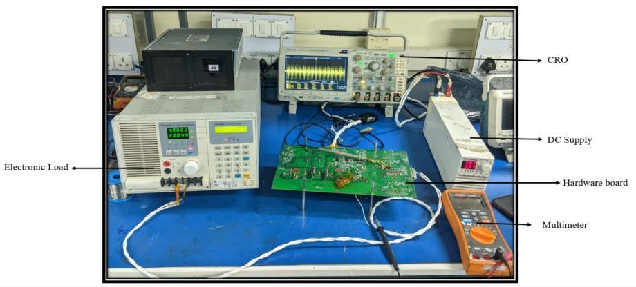
Table4:Ripplevoltageforvariesloadandinput
D. Load regulation and Line regulation
Table2:Outputvoltagesofdifferentloadsanddifferent voltages
Table5:Regulationoflineandload
Table6:VoltageofVDSandVGSfordifferentinput
International Research Journal of Engineering and Technology (IRJET) e-ISSN: 2395-0056
Volume: 11 Issue: 08 | Aug 2024 www.irjet.net p-ISSN: 2395-0072
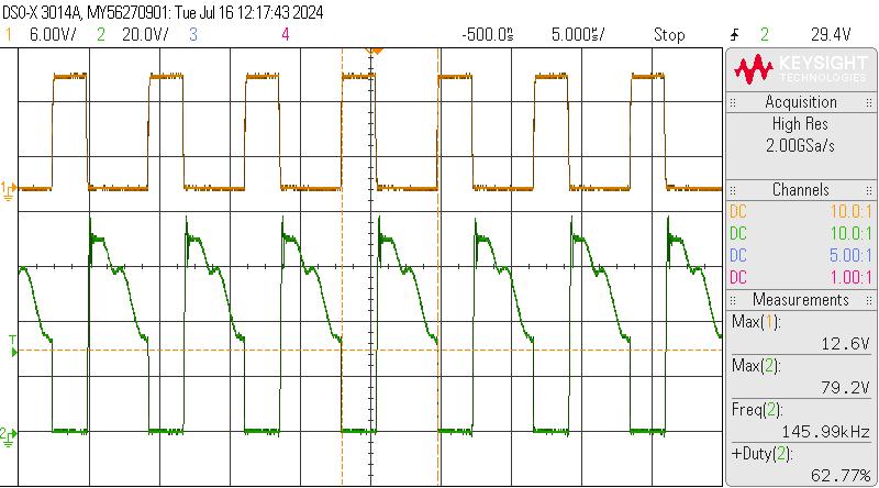
MOSFET Gate to Source and Drain to Source at the nominalvoltage36withfullloadof2AisshowninFig8.
V. Conclusion
TheEfficientDCDCConverterwithForwardConverterfor Low Power Application is designed. The main topology used is Forward converter with the single out of 5V and 2A with the total power of 10 watts. The main components used are Driver circuit , PWM Controller IC , Transformer , MOSFET . The hardware implementation results show results are obtained as per the specification withefficiencyof73%.Thevoltageripplelessthan50mV and the line regulation is below 1% even the Load regulation is also below 1%. The efficiency and the feed forwardPWM techniquecanbeimprovedinfuture.
Reference
1. J. -E. Park, J. -K. Han, S. -H. Choi and G. -W. Moon, "Two-Switch Forward Converter With an Integrated Buck Converter for High Bus Voltage in Satellites," inIEEE Transactions on Power Electronics, vol. 38, no. 2, pp. 2041-2051, Feb. 2023, doi: 10.1109/TPEL.2022.3197610
2. G. Zhou, Q. Tian and H. Li, "Three-Port Forward Converters With Compact Structure and Extended Duty Cycle Range," inIEEE Transactions on IndustrialElectronics,vol.70,no.1,pp.566-581,Jan. 2023,doi:10.1109/TIE.2022.3152015
3. S. K. Tummala and L. Duraiswamy, "Switched Mode Power Supply: A High Efficient Low Noise Forward Converter Design Topology,"2022 IEEE 2nd International Conference on Sustainable Energy and Future Electric Transportation (SeFeT), Hyderabad,
India, 2022, pp. 1-5, doi: 10.1109/SeFeT55524.2022.9908809.
4. J. Rodríguez, J. R. García-Meré, D. G. Lamar, M. M. HernandoandJ.Sebastián,"HighStep-DownIsolated PWM DC–DC Converter Based on Combining a Forward Converter With the Series-Capacitor Structure," inIEEE Access, vol. 11, pp. 131045131063,2023,doi:10.1109/ACCESS.2023.3334794
5. S. Thongmark and W. Wattanapanitch, "Design of a High-Efficiency Low-Ripple Buck Converter for LowPower System-On-Chips," inIEEE Access, vol. 11, pp. 122566-122585, 2023, doi: 10.1109/ACCESS.2023.3328772
6. Y. Zhang, Z. Lian, W. Fu and X. Chen, "An ESR QuasiOnlineIdentificationMethodfortheFractional-Order Capacitor of Forward Converters Based on Variational Mode Decomposition," inIEEE TransactionsonPowerElectronics,vol.37,no.4,pp. 3685-3690, April 2022, doi: 10.1109/TPEL.2021.3119966
7. Phillips,T.Cook,B.WestandB.M.Grainger,"Gallium Nitride Efficacy for High-Reliability Forward Converters in Spacecraft," inIEEE Journal of Emerging and Selected Topics in Power Electronics, vol. 10, no. 5, pp. 5357-5370, Oct. 2022, doi: 10.1109/JESTPE.2022.3175934
8. S.-G.Ryu,S.-Y.Hong,C.-B.Park,H.-W.LeeandJ.-B. Lee, "Design Approach of Planar Transformer-Based 2-TR Phase-Shift Full-Bridge Converter for High Efficiency and High Power Density in LDC," inIEEE Access, vol. 12, pp. 103880-103894, 2024, doi: 10.1109/ACCESS.2024.3434602
9. H. Wu and Y. Xing, "Families of Forward Converters Suitablefor WideInputVoltageRangeApplications," inIEEE Transactions on Power Electronics, vol. 29, no. 11, pp. 6006-6017, Nov. 2014, doi: 10.1109/TPEL.2014.2298617
10. M. Alramlawi and P. Li, “Design optimization of a residential PV-battery microgrid with a detailed battery lifetime estimation model,” IEEE Trans. Ind. Appl.,vol.56,no.2,pp.2020–2030,Mar./Apr.2020
11. Z. Wang, Q. Luo, Y. Wei, D. Mou, X. Lu and P. Sun, "TopologyAnalysisandReviewofThree-PortDC–DC Converters," inIEEE Transactions on Power Electronics, vol. 35, no. 11, pp. 11783-11800, Nov. 2020,doi:10.1109/TPEL.2020.2985287
© 2024, IRJET | Impact Factor value: 8.315 | ISO 9001:2008
| Page681
International Research Journal of Engineering and Technology (IRJET) e-ISSN: 2395-0056
Volume: 11 Issue: 08 | Aug 2024 www.irjet.net p-ISSN: 2395-0072
12. D.ShanmugamandK.Indiradevi,"Implementationof multiport dc-dc converter-based Solid State Transformer in smart grid system,"2014 International Conference on Computer Communication and Informatics, Coimbatore, India, 2014,pp.1-6,doi:10.1109/ICCCI.2014.6921847.
13. J. Zeng, W. Qiao and L. Qu, "A LCL-resonant isolated multiportDC-DCconverterforpowermanagementof multiple renewable energy sources,"2013 IEEE EnergyConversionCongressandExposition,Denver, CO, USA, 2013, pp. 2347-2354, doi: 10.1109/ECCE.2013.6647001
14. D.Costinett,D.MaksimovicandR.Zane,"Designand Control for High Efficiency in High Step-Down Dual Active Bridge Converters Operating at High Switching Frequency," inIEEE Transactions on PowerElectronics,vol.28,no.8,pp.3931-3940,Aug. 2013,doi:10.1109/TPEL.2012.2228237
15. H.-f.WuandY. Xing,“Afamilyofforwardconverters withinherentdemagnetizingfeaturesbasedonbasic forward cells,” IEEE Transactions on Power Electronics,vol.25,no.11,pp.2828–2834,2010.