
International Research Journal of Engineering and Technology (IRJET) e-ISSN:2395-0056
Volume: 11 Issue: 09 | Sep 2024 www.irjet.net p-ISSN:2395-0072

International Research Journal of Engineering and Technology (IRJET) e-ISSN:2395-0056
Volume: 11 Issue: 09 | Sep 2024 www.irjet.net p-ISSN:2395-0072
Sumeet G Zalaki1 , Dr. Anitha G S2 , Santosh B L3, Bhoopendra Kumar Singh4
1P G Student, RV College Of Engineering, Bengaluru
2Associate Professor, RV College Of Engineering, Bengaluru
3Assistant Manager, Centum Electronics Limited, Bengaluru
4Director, Centum Electronics Limited, Bengaluru
Abstract - power supply module (PSM) is widely used in modern power electronics to deliver power to the different applications. In this paper, the use of forward converter topology to design step-down dc-dc converter with the help of transformer (to provide isolation between the input and the output) is proposed for application that require low output ripple, high output current and high conversion ratio. The proposed converter uses new generation SiC MOSFET’s in parallel that have good efficiency and better conduction losses. The operating principle and design producers are presented together with analysis. The selected topology provides a better conversion with less ripple voltage at the output, by which the overall energy stored in the inductor can be decreased and/or increase the efficiency of the converter. The circuit is provided with under voltage protection for which the converter shuts down below the minimum voltage. The converter operation is validated for 80W with 5V/8A for each output, which is simulated in LTSPICE & hardware is successfully tested at 150KHz operating frequency.
Key Words: power supply module (PSM), forward converter, high step-down dc-dc converter, under voltageprotection,operatingfrequency
Power supply module is an interface between power sourceandtheelectronicload.Theprimarypurposeofthe power supply unit is to modulate or convert the available electrical energy from the power supply into the form required by the load [1]. It is quite rare that the power source directly matches the requirements of a particular load.So,thepowersupplyunitsfindextensiveapplications that play a crucial part in modern power electronics (like batteryoperateddevices,powersupplydesign,renewable energy system, etc.) that require high conversions ratio. Typically, a high step-down transformer with isolated Pulse-Width-Modulation (PWM) IC plays a major part in thevoltageconversion[2-4]
DC/DC converters are known as power converters that convert electrical power provided from a source at a certainvoltageleveltoelectricalpoweratadifferentlevel, often providing a regulated output. Various applications like power supplies for computers, various consumer electronic goods, uninterrupted power supplies [UPS], telecommunication units and so on by the DC/DC converters. Regulated DC power supplies are required for better and efficient operation of electronic systems. Most of the power supply are designed to meet the basic requirementslikeregulatedoutput,electricalisolationand multiple outputs. In addition to these basic requirements, common goals of any power supply design are to reduce thesize,weightandtoincreaseefficiency[5-7]
The use of SiC MOSFET’s in parallel provides the converters topology with good current handling capacity with the benefits of faster switching characteristics and lower on-state resistance, leading to improved efficiency. The main benefit of the forward converter topology is its increased efficiency over other topologies as a result of lowerswitchingandconductionlosses.Electricalisolation between input and output stage is necessary for applicationwheresafetyisparamount[8]
The transformer used in the converter is modelled with magnetizing inductance and dependent sources. By implementing forward converter with wide input range, thecurrentdistributionacrosstheparallelMOSFET’s,high efficiency, low switching losses etc, is achieved [9]. The converterisapplicablewiththebenefitsinmediumtohigh powerapplicationwiththepowerratingoflessthan200W and which require high efficiency with optimal switching condition [10]. The block diagram of the forward dc-dc converterasshowninFig-1.
International Research Journal of Engineering and Technology (IRJET) e-ISSN:2395-0056
Volume: 11 Issue: 09 | Sep 2024 www.irjet.net p-ISSN:2395-0072
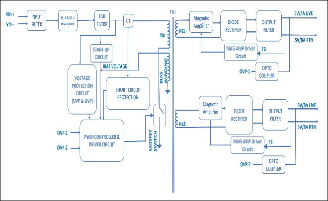
Fig-1 Blockdiagram
Therestofthepaperisorganizedasfollows.Thetopology is described and analyzed in Section II. The specification and design is provided in Section III The experimental resultsaregiveninSectionIV.Finally,SectionVconcludes thispaper.
2. TOPOLOGY SELECTION AND PRINCIPLE OF OPERATION
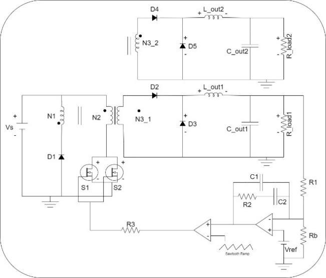
Fig-2 proposedtopology
2.1. Topology selection:
The proposed converter for the application consists of a forward converter with a parallel MOSFET’s anddualoutputisshowninFig-2.
Derived from the buck topology, the single MOSFET forward converter employs a transformer that helpsto providegalvanicisolationaswell asvoltagestepup or step-down, which makes good choice for applications requiring both. The single active switch is
sufficientatlowerpowerlevelsbelow50Wandtwoactive switches connected in parallel can used for application which are greater than 50W and less then 200W, where component stresses are modest and a half- or full-bridge type topology is not needed. This type of converter is commonly used in applications requiring both high efficiency and stability, by providing electrical isolation throughthetransformer.
Includestwomodesofoperation.
(a) Mode 1: This mode is during the time duration whentheswitchis“ON”.
(b) Mode 2: This mode is during the time duration whentheswitchis“OFF”.
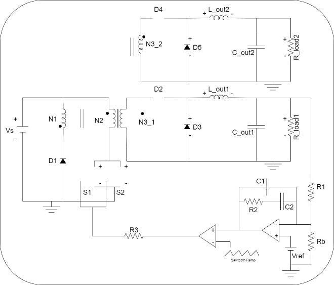
1. Mode1:Theswitchisclosed,andvoltageatinputis applied across the primary winding of the transformer. Primary current starts to flow. The equivalentcircuitisasshowninFig- 2.1.Duetodot polarityoftransformera voltageappearsacross the secondary winding and energy is transferred from primarytosecondary.Thecurrentandvoltageatthe primary and secondary are related through the turn’sratio(N3/N2)ofthetransformer.
Fig-2.1 Forwardconverterequivalentcircuitduring mode1.
As the switch is closed, the forward diode D2& D4 becomes forward biased, and transformer secondary side voltage appears across a low pass filter constituted by L and C. The high frequency ripple is filtered by the low pass filter and output is
International Research Journal of Engineering and Technology (IRJET) e-ISSN:2395-0056
Volume: 11 Issue: 09 | Sep 2024 www.irjet.net p-ISSN:2395-0072
delivered to the load. The freewheeling diode D3& D5 remainsOFFasit’sreversebiasedbythepositive voltage appearing across its cathode. This mode is thepoweringmodeastheinputpoweristransferred to the load. Because of the opposite dot polarity, diodeD1 isreversebiasedandremainsOFF.
2. Mode 2: It is freewheeling mode. This mode begins when the switch opens. The transformer current fallstozero.Butthefilterinductoratsecondaryside maintains a continuous current through load throughthefreewheelingdiodeD3&D5.Theforward diode D2& D4 remains OFF during this state. Due to opposite dot polarity of reset and primary winding, diodeD1 conductsandthemagnetizingcurrentflows in reverse direction, thus resetting the core. The equivalentcircuitisasshowninFig-2.2.
3. SPECIFICATION AND DESIGN OF THE PROPOSED SYSTEM
3.1 Specification:
Thedesignspecificationoftheforwardconverter isrepresentedinTable-1.
Table-1 ConverterSpecification
InputVoltage 30V–42VDC
Topology IsolatedForward Converter
(Vout1& Vout2)
(Iout1& Iout2)
3.2 Design equations:
Mode1:
Theequationsgoverningthemode1areasfollows:
VoltageacrosstheprimarywindingNp isgivenby,

(3.1)
VoltageacrosstheresetwindingNrisgivenby,

(3.2)
VoltageacrossthesecondarywindingNsisgivenby,

(3.3)
VoltageatthecathodeofDiodeD1 isgivenby,

Voltagethroughoutputinductorisgivenby,
(3.4)

(3.5)
Currentflowingthroughtheoutputinductorincreasesand isgivenby,

Mode2:
(3.6)
Theequationsgoverningthemode2areasfollows:
VoltagethroughresetwindingNrisgivenby,

(3.7)
VoltagethroughprimarywindingNp isgivenby,

(3.8)
International Research Journal of Engineering and Technology (IRJET) e-ISSN:2395-0056
Volume: 11 Issue: 09 | Sep 2024 www.irjet.net p-ISSN:2395-0072
Maximum voltage across the switch Q is given by the equation, (3.9)

VoltageatsecondarywindingNs isgivenby, (3.10)

Voltageacrosstheoutputinductorisgivenby, (3.11)
Current through the output inductor decreases and is givenby,


(3.12)
From Volt-Second balance adding equation 2.6 and 2.11 andequatingittozero,theoutputvoltageisobtainedas, (3.13)
Where,
Vin(Vs):Inputvoltage
Np(N2):Numberofturnsinprimarywinding
Nr(N1):Numberofturnsinresetwinding
Ns (N3_1 & N3_2) : Number of turns in the secondary winding
VD3(VD1): dropVoltageacrossdiodeD3
D:Dutyratio
T:Timeperiod
VD1(VD2&VD4):dropVoltageacrossdiodeD1
VQ(Vs1&Vs2):VoltageacrossswitchQ
Vout(Vout&Vout_1):Outputvoltage
4.1 simulation results:
To observe the performance of the converter developed,asimulationcircuitisdevelopedintheLT-spice asshowintheFig-3
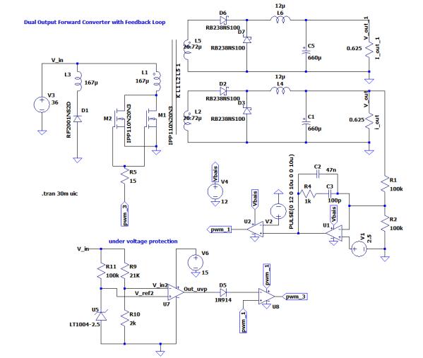
Fig-3 Forwardconvertersimulationcircuit
The simulation waveforms are shown in Fig-3.1, which includes output voltage and output current for both the outputsatnominalvoltage(i.e.36V).

Fig-3.1 Forwardconverteroutputvoltage¤tfor boththeoutputs
4.2 Hardware results:
Fig-4showsthehardwareexperimentalset-upforforward converter. The main components of set-up circuit are as follows:
Powersupply
DigitalCRO
Forwarddc-dcconverter
Electronicload
International Research Journal of Engineering and Technology (IRJET) e-ISSN:2395-0056
Volume: 11 Issue: 09 | Sep 2024 www.irjet.net p-ISSN:2395-0072
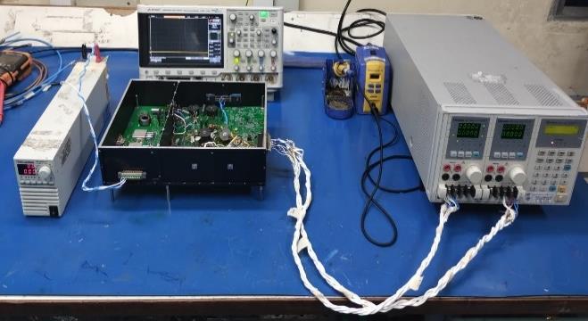
Fig-4 experimentalset-up
Thetopviewandbottomviewoftheforwardconverteras shown in Fig-4.1 & Fig-4.3 The main components of the forwardconverterinthehardwaresetupareasfollows:
EMIfilter
Maintransformer
MOSFET
Biasinductor
Secondarydiodes
Magneticamplifier
Outputinductors
PWMIC&DriverIC
Outputcapacitors
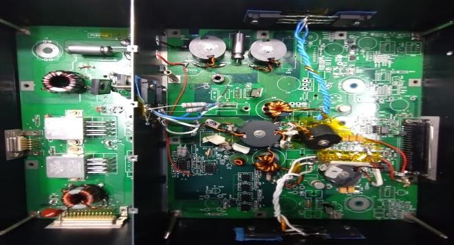
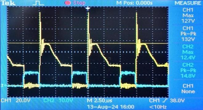
Fig-4.2 shows the gate and drain pulse of the MOSFET in theconverteratthenominalvoltage(i.e.36V).
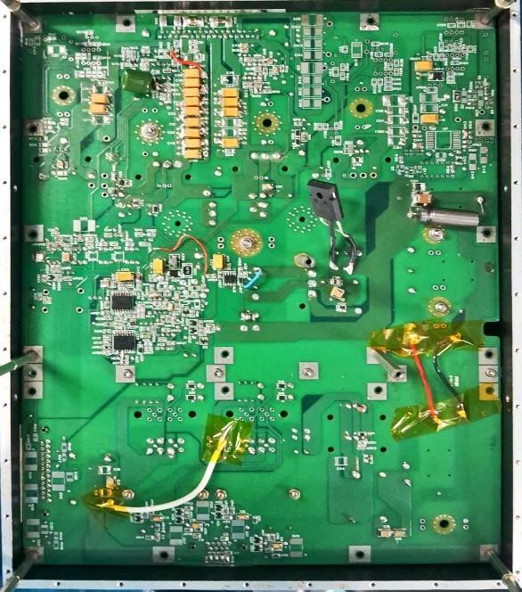
Fig-4.4 shows the output voltage of the tested converter, (as both output are same i.e. 5V) for the nominal voltage (i.e.36V).

Table-2 VDS,VGS &Dutycycleatdifferent inputcondition
International Research Journal of Engineering and Technology (IRJET) e-ISSN:2395-0056
Volume: 11 Issue: 09 | Sep 2024 www.irjet.net p-ISSN:2395-0072
Table-3 outputvoltageat100%loadfordifferentinput conditionandefficiency
Input
Table-2showstheresultsofthegateanddrainvoltagefor different input conditions with duty cycle that is been measured during the testing of the hardware. Whereas Table-3 show output voltage at 100% load condition and inputcurrentatdifferentinputvoltagecondition.
The hardware implementation and test results of the converter are presented. The analysis shows that the converter is operating at efficiency greater than 65% according to the specification. At maximum load conditions an efficiency of 67.17 % is achieved. Line regulation is less than 1%, load regulation and cross regulation less than 2% and thus meet the specifications. Gate, drain and output waveform for varies voltages are presented and analyzed. The experimental observations obtained under input and load conditions validate and justifythedesigntotheproposedtopology.
I deeply express my heartfelt thanks to my guide Dr. Anitha G S, Associate professor, Dept. of EEE, RVCE, Principal and HOD, Dept. of EEE, RVCE and panel members for their essential guidance throughout the project. Also I would like to express my deepest appreciation to Centum Electronics Limited, Bengaluru to provide me an opportunity to carry out the project in their organization and help me to gain hands on experienceabouttheproject.
[1] J. Rodríguez, J. R. García-Meré, D. G. Lamar, M. M. Hernando and J. Sebastián, "High Step-Down Isolated PWM DC–DC Converter Based on Combining a Forward Converter With the Series-
Capacitor Structure," in IEEE Access, vol. 11, pp.
131045-131063,2023.
[2] X. Zhang, B. Nguyen, A. Ferencz, T. Takken, R. Senger, and P. Coteus, ‘‘A 12- or 48-V input, 0.9-V output active-clamp forward converter power block for servers and datacenters,’’ IEEE Trans PowerElectron.,vol.35,no.2,pp.1721–1731,Feb. 2020.S.
[3] M Rodríguez,A Rodríguez,P.F Miaja,D.G Lamar and J. S. Zúniga, "An Insight into the Switching Process of Power MOSFETs: An Improved Analytical Losses Model," in IEEE Transactions on Power Electronics, vol 25, no. 6, pp 1626-1640, June2010
[4] P. Rehlaender, F Schafmeister, and J Böcker, ‘‘Interleaved single-stage LLC converter design using half- and full-bridge configurations for wide voltage transfer ratio applications,’’ IEEE Trans. Power Electron., vol 36, no 9, pp 10065–10080, Sep.2021.
[5] e, Y Lei, and R C N Pilawa-Podgurski, ‘‘The cascaded resonant converter: A hybrid switchedcapacitor topology with high power density and efficiency,’’IEEETrans.PowerElectron.,vol.35,no. 5,pp.4946–4958,May2020
[6] S. Jiang, S. Saggini, C Nan, X Li, C Chung, and M Yazdani, ‘‘Switched tank converters,’’ IEEE Trans. PowerElectron.,vol 34,no.6,pp 5048–5062,Jun 2019.
[7] Z. Ye, S. R. Sanders, and R. C. N. Pilawa-Podgurski, ‘‘Modeling and comparison of passive part volume of hybrid resonant switchedcapacitor converters,’’ IEEE Trans Power Electron., vol 37, no. 9, pp. 10903–10919,Sep.2022
[8] S. Biswas, D. Reusch, and M de Rooij, ‘‘Design of GaN-based multilevel switched capacitor converters Benefits and challenges,’’ IEEE Trans. Ind.Appl.,vol.56,no.2,pp.979–988,Mar.2020.
[9] H. Cao, X. Yang, C. Xue, L. He, Z. Tan, M. Zhao, Y. Ding,W Li,andW Qu,‘‘A12-levelseries-capacitor 48–1 V DC–DC converter with on-chip switch and GaN hybrid power conversion,’’ IEEE J Solid-State Circuits,vol 56,no.12,pp.3628–3638,Dec 2021
International Research Journal of Engineering and Technology (IRJET) e-ISSN:2395-0056
[10] D.-V. Bui, H. Cha, and V.-C. Nguyen, ‘‘Asymmetrical PWM seriescapacitor high-conversion-ratio DC–DC converter,’’ IEEE Trans. Power Electron., vol. 36, no.8,pp.8628–8633,Aug.2021.
Volume: 11 Issue: 09 | Sep 2024 www.irjet.net p-ISSN:2395-0072 © 2024, IRJET | Impact Factor value: 8.315 | ISO 9001:2008 Certified Journal | Page34