
International Research Journal of Engineering and Technology (IRJET) e-ISSN: 2395-0056
Volume: 11 Issue: 09 | Sep 2024 www.irjet.net p-ISSN: 2395-0072

International Research Journal of Engineering and Technology (IRJET) e-ISSN: 2395-0056
Volume: 11 Issue: 09 | Sep 2024 www.irjet.net p-ISSN: 2395-0072
Santoshkumar Gadigeppa Asooti1 , Dr. Parth Sarathi Panigrahy2 , Narendrababu HB3 , Bhoopendra Kumar Singh4
1First Author Affiliation & Address1P G Student, RV College of Engineering, Bengaluru
2Assistant Professor, RV College Of Engineering, Bengaluru
3Assistant Manager, Centum Electronics Limited, Bengaluru 4Director, Centum Electronics Limited, Bengaluru
Abstract - Anelectricalloadisenergizedbyapowersource designed to precisely convert input current into the specific voltage, current, and frequency required for device functionality. Optimized transformer design is employed to minimizeleakage inductance inthecore winding,focusing on reducing energy loss, enhancing efficiency, and decreasing overallsizeandweight.Switched-modepowersupplies(SMPS) are superior to linear supplies in achieving these objectives, with forward topology being particularly suited for low to medium-power applications due to its simplicity, costeffectiveness, and ease of adding multiple outputs. However, forward topology presents challenges such as suboptimal cross-regulation and high voltage stress on the MOSFET switch, which are mitigated through the use of snubber circuits and coupled inductors. This project endeavors to design a triple-output forward converter with integrated protectioncircuitstoenhance reliability.UtilizingtheUC2825 PWM IC for primary side voltage mode control, the converter operates at a 500 KHz switching frequency. The final design, incorporating coupled inductors for improved regulation, achieves the targeted 82% efficiency.
Keywords: Transformer Design, MOSFET Selection, External Synchronous Circuit, Coupled Inductors Topology,UC2825PWMIC,UC2901IsolatedFeedbackIC &Efficiency
Switched-Mode Power Supplies (SMPS) offer advantages like higher efficiency, better voltage regulation,compactsize,andmultipleisolatedoutputs, makingthemapreferredreplacementforlinearpower supplies.SMPSregulatespowerdeliverythroughthe on-offswitchingofsemiconductortransistors.Forlowoutputpowerapplications(afewwattstounder100watts) with isolated inputs and outputs, forward converter topology is simpler and cost-effective, despite being less efficientthanotherSMPScircuits.Forwardconvertersuse outputinductanceandfreewheelingdiodes,andPulseWidth Modulation (PWM) control is employed to maintain
regulated output voltage by varying the MOSFET's duty cycle.Inthisproject,theUC2825PWMICisusedforvoltage modecontrol,providingsimpleforwardcontrol,improved cross regulation, and a good noise margin. However, for betterloadandcrossregulationinmulti-outputconverters, coupled inductors are used. This triple-output forward converter is being designed for space applications, where reduced size, weight, and high reliability are critical. The design achieves the targeted efficiency of 82% as per the specifications.
Table1showsthespecificationsoftheConverter.
Table.1: Converter Specifications
Parameter
InputVoltageRange
Specifications
60V-100VDC
NominalInputVoltage 70VDC
Topology ForwardDC-DCIsolated Converter
SwitchingFrequency 500KHz
OutputVoltage& Current 5V/4A +15V/0.667A -15V/0.667A
Volume: 11 Issue: 09 | Sep 2024 www.irjet.net p-ISSN: 2395-0072
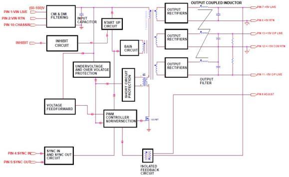
Theschematicrepresentationofthetripleoutputforward converterisdepictedinFigure1.Thesystemcomprisesan inputsection,acontrolsection,aprotectionsection,andan outputstage.Inadditiontothebiasvoltagecircuitderived from the auxiliary winding of a transformer, the input sectionalsoincorporateselectromagneticinterference(EMI) filters,astart-upcircuit,andseveralothercomponents.An integratedcircuit(IC)forPWMcontrol,aMOSFETswitch, and input from the bias winding constitute the control section. Output short circuit safety, input undervoltageprotection,andoutputovervoltageprotection.
Allvoltageprotectionmeasuresareencompassedwithin theprotectionsection.Toprovideisolationamongthethree outputs,eachoutputisassignedadistinctgroundpotential. Anelectromagneticinterference(EMI)filterinterceptsthe input voltage and eliminates noise in both the differential and common modes. The initial power supply for the UC2825PWMICisderivedfromthestart-upcircuit.Once the converter is completely operational, the bias voltage, whichexceedsthestart-upvoltage,willreplacethestart-up circuit.Here,acurrentsenseresistorquantifiestheprimary sidecurrentprovidedtotheUC2825integratedcircuit(IC) andcomparesittothefeedbackerrorsignalfromthebias voltage feedback. This comparison generates pulse width modulation (PWM) signals that control the main MOSFET switch.Byadjustingthegainandcutofffrequenciesofthe PWM integrated circuit, the switching frequency of the converterissubsequentlyadjustedto500kHz. Toprovide the required RAW voltages, the secondary side outputs undergocorrectionandfilteringbytheirrespectiveSchottky diodes and output capacitors. The RAW voltages are transmitted to the corresponding linked inductors to generate the precisely controlled outputs of 5V/4A, +15V/0.667A,and-15V/0.667Aintheoutputstage.Inthe eventofanyfailuresorabnormalsituationsintheprotection circuits, the shutdown pin of the PWM IC is latched to inactivatetheconverter.Furthermore,theconverterwillnot functionunlesstheinputundergoesreprocessing.
Anappropriatecorewillbeselectedwhichmusthavean area productgreaterthanthecalculatedAp.Area product (Ap)isgivenastheproductofthecorecrossselection(Ac) andthewindowarea(Aw).Thesedataareavailablein the ferrite magnetic core design catalog. The area product methodisusedtocalculatethesizeofapowertransformer.
TheselectedcoreisYP-41605-TC,Material:P,Ur:2500with ����:1375mH/1000T.
Ap=Ac∗Aw (1)
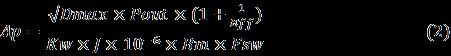
Where, Window factor, ���� = 0.4, Current density, J = 4Amp/����2,Fluxdensity,����=0.1Tesla,Pout=41.21W
TurnsRatio,


The choice of MOSFET is contingent upon several factors, includingtheDrain-Sourcevoltage(VDS),Draincurrent(Id), Drain-SourceONresistance(Rds_on),Gatecharge(Qg),and OutputCapacitance(Coss).Theselectionanddimensionsof aMOSFETaredeterminedbythelossesthatoccurwithinit.

SELECTEDIPP60R125CP/BUY65CS08J,650V,25A, 125mOhm,PG-TO220.
ThesecondaryoutputvoltageofTransformersisrectified and filtered in order to achieve the desired output parameters.TheproposedconverterutilizesanLCfilter,and itiscrucial toselecttheoptimal valuesforthisfilter.This ensures that the converters have minimal noise, are compact, and cost-effective, which are the primary requirementsforSpaceapplications.
International Research Journal of Engineering and Technology (IRJET) e-ISSN: 2395-0056
Volume: 11 Issue: 09 | Sep 2024 www.irjet.net p-ISSN: 2395-0072

The selection of the output diode is contingent upon the magnitude of the secondary current and voltage. The essential requirement for these diodes is that they must operateathighfrequencies.Duringthetransitionfromthe ON state to the OFF state, the reverse recovery time of a standardsignalorp-ndiodetypicallyrangesintheorderof hundredsofnanoseconds.
However,forfastrecoverydiodes,thisperiodislessthan 100nanoseconds.Ontheotherhand,Schottkydiodeshave anextremelylowreverserecoverytime,almostnil.Schottky diodesareveryappropriate duetotheirminimal forward voltage drop (VFD), high current capacity (IF), and low reverserecoverytime(Trr)
Selected diode1 is 35CGQ100, 100V, 16A, 16CYQ100C (Industrial),and a SC105H100SCDV
Selecteddiode2is400V,4A,1N6627
Selected diode3 is 16CYQ150 (Industrial), 150V, 16A, SC125H150ACDV
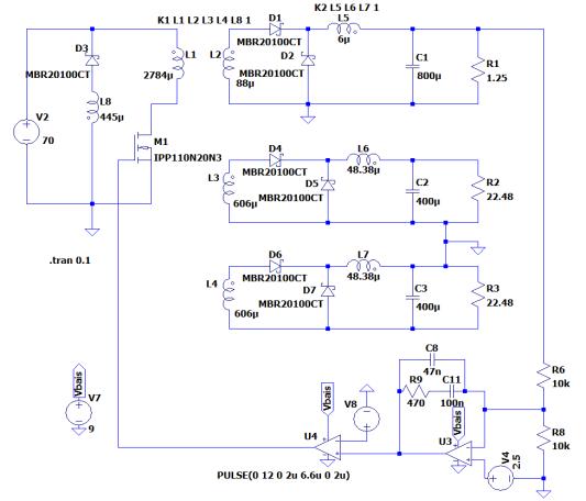
A feedback path is provided to the system to improve its transient and steady-state response. A voltage controller with type 2 Compensation Technique is employed as feedback. Simulation is essential for any system's initial design.Simulationcanbeusedtopredictsystembehavior andperformance.Theoutput-regulatedclosedloopsystem isdesignedinLTspicesoftwareasshowninFig2
SimulationwaveformisshowninFig-3,whichincludesthe firstOutputvoltageof5V
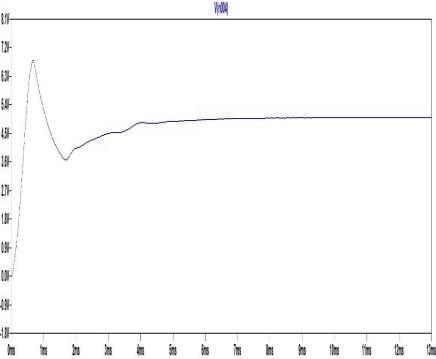
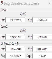
Fig-3: FirstOutputVoltage
ThesimulationwaveformisshowninFig-4,whichincludes thesecondOutputvoltageof+15V
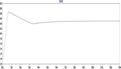
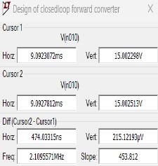
Fig-4: SecondOutputVoltage
ThesimulationwaveformisshowninFig-5,whichincludes thethirdOutputvoltageof-15V
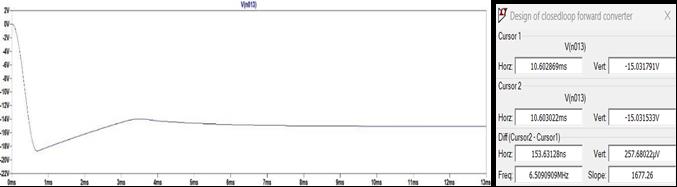
Fig-5: ThirdOutputVoltage
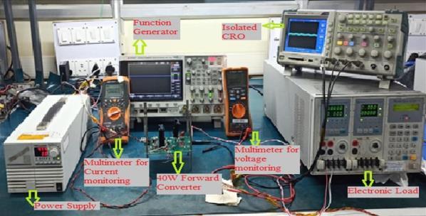
The experimental setup for the triple-output forwardconverterisdepictedinFig-6.Componentsofthe experimental setup include a digital storage oscilloscope (DSO), converter, electronic load, pulse generator, multimeter,andinputpowersupply.Regulationoftheinput voltageispossiblewithin60to100voltsattheminimum, nominal,andmaximumloadlevels.Thetableabovedisplays the statistical measures of efficiency, line regulation, load regulation, cross-regulation, and ripple voltages. Tabular formatdisplaysthetestresultsobtainedunderfullload.
International Research Journal of Engineering and Technology (IRJET) e-ISSN: 2395-0056
Volume: 11 Issue: 09 | Sep 2024 www.irjet.net p-ISSN: 2395-0072
As shown in Table 2 below, the output voltage is determinedatvaryinginputvoltagesandloadconditions At theminimumandthemaximumvalues,inputcurrent,input power,andoutputpower,efficiencyareobservedtobe82%.
Table -2: Outputvoltagesatfullloadfrom60V-100V inputvoltages&efficiency
LineRegulationinTable4islessthan1%asmentionedinthe specification
Table -4: LineRegulationatfullload
TheripplevoltageinTable-3isunder50mVasmentionedin thespecification
Table -3: Outputripplevoltagesat100%loadfrom60V100Vinputvoltages&efficiency
LoadRegulationinTable5islessthan2%asmentionedin thespecification
Table -5: Outputripplevoltagesat100%loadfrom60V100Vinputvoltages&efficiency
Regulation (%)
(V)
O/P +15V O/P -15V O/P Vout1 Vout2 Vout3
16 18 28
30.4 22 22
16 24 22
The 40W DC-DC triple output forward converter has ripplesthatallarewithinspecificationlike30.4mV,22mV, and22mVatmaximumloadandnominalvoltageisshownin Fig.-7
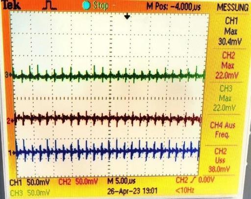
Fiig-7:InputVoltage: 70V,CH1:5V/4A,CH2: +15V/0.667A,CH3:-15V/0.667A
AsshowninFig.5,theMOSFETgatevoltageoutput waveformofthe40WDC-DCtripleoutputforwardconverter has a gate voltage of 10.2V, which is within the specified range.
International Research Journal of Engineering and Technology (IRJET) e-ISSN: 2395-0056
Volume: 11 Issue: 09 | Sep 2024 www.irjet.net p-ISSN: 2395-0072
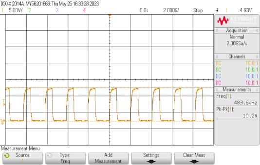
Fig-8: InputVoltage: 70V,Nom.GateVoltage:10.2V
The 40W DC-DC triple output forwardconverter's MOSFET drain voltage output waveform is illustrated in Fig.6 with a full load and the nominal voltage, and it is withinspecificationswitha129Vdrainvoltage.
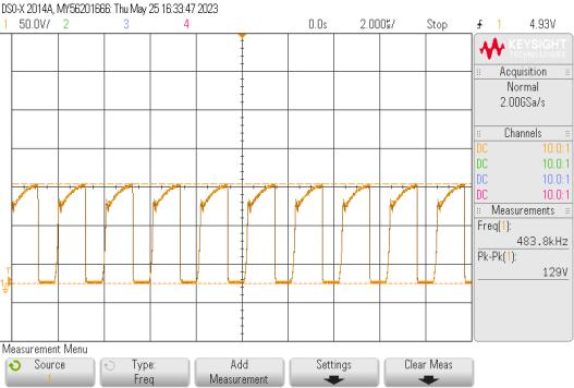
Fig-9: InputVoltage:70V,Nom.DrainVoltage:129V
3. CONCLUSIONS
Thisstudypresentstheimplementationofatripleoutput isolatedforwardconverterusingthevoltagemodecontrol approachandlinkedinductoraspostregulators.Optimally builtpost regulators effectivelycontrol output voltages to fall well within the intended range. Based on the experimentally verified experimental findings obtained at fullload100%withdifferentinputvoltages,itisevidentthat the output ripple, MOSFET stress, Diode stress, Line regulation,and Load regulation all meet the specified requirements. The implementation of a snubber circuit enhancestheoverallefficiencyoftheconverterby4-5%.A potential area for further study is enhancing the digitally controlledMOSFETfeedforward.
Thisanalysisisspecifictospaceapplications.Thehardware verificationofthedesignfollow-uphasbeenconductedfor allthreeoutputs.Thesimulationandhardwareexperimental findings,aswellasthewaveforms,arepresented.
[1] S.Zaharieva,I.Stoev,A.Borodzheva,S.Stoyanov,”Studyof SwitchingForwardSingleEndedDC-DCConverterinthe Course Power Supplies”, 2020 43rd International Convention on Information, Communication and ElectronicTechnology(MIPRD).M.Young,TheTechnical Writer’sHandbook.MillValley,CA:UniversityScience, 1989.
[2] SoumyaK,ArpithaRajuB,BhanuprakashCV,B.K.Singh, “SingleOutput40WDC-DCForwardConverterforSpace Application”, 05 May 2022 International Research JournalofEngineeringandTechnology(IRJET).K.Elissa, “Titleofpaperifknown,”unpublished.
[3] Nagesh L, Bhanuprakash CV, B.K.Singh, Vinod Chippalakatti, “Design and implementation of Triple OutputForwardDC-DCConverterwithCoupledInductor as Post-Regulator for Space Application,” 2020 International Conference on Smart Technologies in Computing,ElectricalandElectronics(ICSTCEE).
[4] Aravind Bhat, K.Uma Rao, Praveen PK, Bhoopendra Kumar Singh, Vinod Chippalkatti,”Multiple Output ForwardDC-DCConverterwithRegenerativeSnubberfor Space Application,” 2016 Biennial International Conference on Power and Energy Systems Towards SustainableEnergy(PESTSE).
[5] SureshKumarTummala,LenineDuraiswamy,”Switched ModePowerSupply:AHighEfficientLowNoiseForward ConverterDesignTopology,”2022IEEE2ndInternational ConferenceonSustainable Energyand FutureElectric Transportation.
[6] Congwen Xu, Qishuang Ma, Ping Xu and Nan Wang,”Closed-Loop Gate Drive for Single-Ended ForwardConvertertoReduceConductedEMI,”26June 2020PublishedinIEEEAccess.
[7] ].G.R.P.Lakshmi,”A Dual-Transformer Active-Clamp Forward Converter using a Single Switch,” 2017 International Conference on Computation of Power, Energy,InformationandCommunication(ICCPEIC).