3 minute read
MATERIALS AUSTRALIA WA Branch Meeting Report - 13 November 2023
How Solar Cells Work at the Atom Scale
Source: Dr Gilles Dour, Advisian
The Western Australia Branch hosted a technical meeting in mid-November. Dr Giles Dour (Principal Integrity Engineer with Advisian) gave a presentation on the topic How solar cells work at the atom scale.
Dr Dour recalled his time as a doctoral candidate in France in the mid-1990s, when he was undertaking research into silicon production for solar cell applications. He has maintained a strong interest in the development of photovoltaics (PV) ever since.
Gilles explained that he had become involved with PV through a family connection. His uncle had founded a solar panel manufacturing business, subsequently sold to EDF. Gilles, who had just completed a Master’s degree in materials engineering, had been just the right person to work on a research project in continuous solidification of PV crystalline silicon. His research extended further into PV manufacturing processes, giving him a solid grounding in the business aspects of PV, and the continuing quest for higher conversion efficiency.
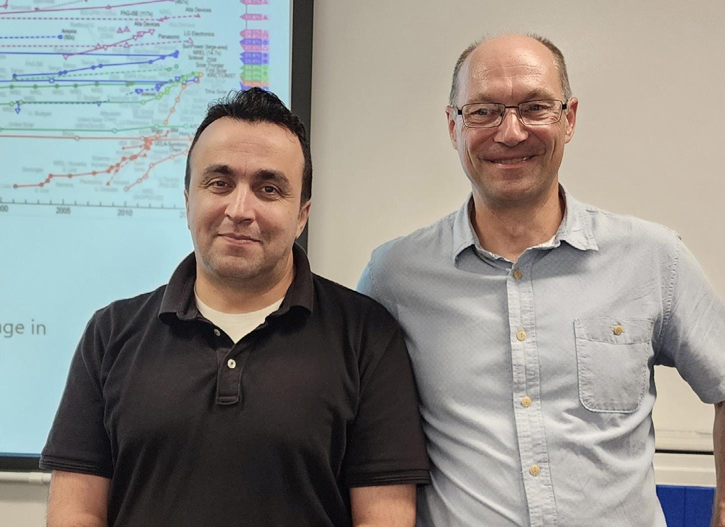
Gilles referred the National Renewable Energy Laboratory (NREL) chart to show the remarkable progress of PV panel efficiency since the 1970s. Each of the silicon-based technologies has shown steady progress, but with step changes between technologies. The efficiency of multi-junction cells has now reached 48% in the laboratory. Some emerging (non-silicon) technologies, although only now approaching 20% efficiency, are advancing at faster rates than silicon technologies.
Gilles’ talk ranged from physics, with the quantised nature of electromagnetic radiation and the relationship between light wavelength and energy, through materials science, and band gaps in semiconductors, on to the materials engineering involved in silicon crystal growth, and then to manufacturing engineering in producing commercial solar PV panels.
The phenomenon at the heart of PV is that when electromagnet radiation of the appropriate wavelength interacts with a semiconducting material, an electron is promoted from the valence band to the conduction band, leaving a positive electron hole. In the absence of an electric field, the electrons and electron holes diffuse separately and at random until they eventually collide and disappear by pair annihilation. Impurities, crystal defects and grain boundaries promote pair annihilation, which is why high-purity single crystal silicon allows higher efficiency, though not necessarily more cost-effective PV cells.
Gilles then outlined the processes using producing high-purity silicon and growing single-crystal ingots.
In explaining this, Gilles noted out the common misconception that the PV phenomenon is a surface effect. In fact, sunlight penetrates silicon to a depth of around 200 μm before it is completely absorbed. This is why the silicon in PV cells is typically in the form of wafers around 250 μm thick.
This led to a description of how silicon ingots are cut into 250 μm wafers; this incurs about 50% wastage, with the waste silicon being diverted to much lower value uses. Gilles went on to describe how he had undertaken research into growing 250 μm ribbons of silicon direct from the melt. These are multi-crystalline, and not as efficient, but much cheaper than single crystal silicon.
Producing free electrons and holes is the start of the process, but the vital step in turning the phenomenon into a useful energy conversion device is creating the cell; this establishes the electric field which imposes a gradient on charge carrier diffusion. The cell is created by doping the silicon so that it is a p-type semiconductor, and then doping a very thin (less than 1 μm) n-type layer, usually on the light-facing (‘top’) surface. Electrical contacts are then formed on the p-type and n-type , typically with a conducting grid, with another electrical connection on the ‘bottom’. These are joined to form a circuit through an electrical load. In the absence of light, this is simply a semiconductor diode, but when light of the right wavelength range falls on the surface and free charge carriers are created in the bulk material, current will flow, with voltage related to current. Holes move through the p-type silicon to the bottom surface, electrons move to the top n-doped surface, are collected, and then flow through the load to return through the bottom connector where they recombine with the holes, thus completing the circuit.
Putting a conducting grid on the surface reduces the light entering the silicon, and hence reduces efficiency. This has led to several other architectures that Gilles summarised briefly. The PERC (passive emitter rear contact) cell developed at UNSW, in now very common, while the IBC (Interdigitated Back Contact) cell, with no contacts on the light-facing surface is another contender. Corrosion of connectors is a major factor in determining the effective life of solar PV panels.
Not all solar PV cells are based on silicon.
The CIGS (Copper, Indium Gallium Selenide) cell has much higher light absorption than silicon, and therefore can be used in thin film form, only around 1 μm thick. These cells can be fabricated in several ways including coevaporation, electrodeposition and by printing. There are several technologies based on hydrogenated amorphous silicon, including multi-junction cells that are effective over wide ranges of light wavelengths.
Among the alternatives, thin film hybrid inorganic-organic materials with the perovskite crystal structure have progressed remarkably in just a few years. These are relatively cheap and easy to manufacture but, at first sight these would hardly seem very practical, as they are relatively unstable in oxygen, moisture, heat and light! Nevertheless, Gilles expressed confidence that these issues would be overcome and that the commercial target of a twenty-year useful life would be achieved.
Silicon is not necessarily the ultimate material for solar PV cells, but the enormous established manufacturing base means that it is likely to remain dominant for a long time.


