

The MEPTEC Report is a Publication of the Microelectronics Packaging & Test Engineering Council
PO Box 1053, Los Altos, CA 94023
+1 (415) 287-3276
Email: rosina@meptec.org
Publisher MEPTEC
Editor Ira Feldman
MEPTEC Executive Director Ira Feldman
MEPTEC Advisory Board
Board Members
Dave Armstrong Advantest
Zoë Conroy Cisco
Abram Detofsky Intel
Neal Edwards AMD
Jaspreet Gandhi Meta
Roger Grace Roger Grace Associates
Ravi Mahajan Intel
Emeritus Advisors
Seth Alavi Sunsil
Anna Gualtieri Elle Technology
Phil Marcoux PPM Associates
Mary Olsson
Herb Reiter eda 2 asic Consulting, Inc., Retired In Memoriam
Joel Camarda Ron Jones
Contributors
Jason Blocklove ECE Ph.D. Candidate at NYU
Ira Feldman Feldman Engineering Corp.
Roger H. Grace Roger Grace Associates
Ron Press Siemens Digital Industries Software
Gaurav Veda Siemens Digital Industries Software
MEPTEC Report Vol. 28, No. 2. Published quarterly by MEPTEC, PO Box 1053, Los Altos, CA 94023. Copyright 2024 by MEPTEC. All rights reserved. Materials may not be reproduced in whole or in part without written permission. MEPTEC Report is sent without charge to members of MEPTEC. For non-members, yearly subscriptions are available for $75 in the United States, $80US in Canada and Mexico, and $95US elsewhere. For advertising rates and information contact Ira Feldman at ira@ meptec.org.

Ira Feldman Executive Director, MEPTEC
Welcome to the “Dog Days of Summer”! Not only is this when the star system Sirius rises as the morning star (hence the name), it is when summer vacations are in full swing in much of North America and Europe. Not to mention the hottest days of summer…
Speaking of hot: Artificial Intelligence (AI) is the topic du jour in terms of reshaping our lives and driving semiconductor industry demand. And the applications that are being built based upon generative AI and machine learning are downright cool! AI has been receiving a lot of attention everywhere including the press and industry events.
MEPTEC recently took a unique look at “AI for Semiconductors” in June. This extremely informative virtual event explored the development and deployment of AI for the design, packaging, and test of semiconductors. In this issue we share the work of Jason Blocklove (New York University) on “How Generative AI Can Simplify Digital Hardware Design” and Ron Press and Gaurav Veda (Siemens) on “Using AI and Domain Knowledge to Simplify Electronics Test and Production” If you enjoy these articles, you can also find the slides and presentations from the event on our website I’d like to thank again all the great presenters as well as our sponsors, ASE Global and AMKOR, who made this event possible!
Roger Grace (Roger Grace Associates) also shares with us the high-level results of their annual “MEMS Industry Commercialization Report Card (Report Card) Study” in this issue. This seminal work has been tracking and guiding the industry for 25 years. Congratulation to Roger and his team for the dedication in achieving this milestone! And for sharing the wealth of knowledge with MEPTEC and the MEMS community.
Development continues for our fall in-person event “Frontiers in Test” which will examine leading edge and emerging test challenges. If you would like to join the Technical Program Committee (TPC) or submit an abstract, please contact us.
I look forward to hearing your suggestions and feedback as to how MEPTEC can best serve you. Please don’t be shy!
Stay Cool!
Ira Feldman Executive Director, MEPTEC
ira@meptec.org
+1 650-472-1192
AEHR RECEIVES
$12.7 MILLION IN ORDERS FOR FOX WAFERPAK™ FULL WAFER CONTACTORS
AEHR TEST SYSTEMS has announced it has received $12.7 million in orders from one of its silicon carbide test and burn-in customers for multiple sets of WaferPak™ full wafer Contactors to be used for production needs for wafer level burn-in and screening of silicon carbide power semiconductors for the electric vehicle market. These WaferPaks are expected to be delivered over the next three months. Aehr’s FOX systems and WaferPaks are currently being used on wafer sizes ranging from 4”, 6”, 8” and 12” wafers and can be configured for a wide range of device applications.
www.aehr.com
AMKOR SIGNS PRELIMINARY MEMORANDUM OF TERMS WITH US DEPARTMENT OF COMMERCE FOR ARIZONA ADVANCED PACKAGING AND TEST FACILITY
AMKOR TECHNOLOGY has signed a non-binding preliminary memorandum of terms with the US Department of Commerce to receive proposed funding as part of the CHIPS and Science Act. Amkor announced last Fall its plans to build its first domestic OSAT facility in Peoria, Arizona. Amkor projects to invest approximately $2 billion and employ approximately 2,000 people at the new facility. Upon completion, this will be the largest outsourced advanced packaging and test facility in the United States.
www.amkor.com
PEEL APART A SMARTPHONE, fitness tracker or virtual reality headset, and inside you’ll find a tiny motion sensor tracking its position and movement. Bigger, more expensive versions of the same technology, about the size of a grapefruit and a thousand times more accurate, help navigate ships, airplanes and other vehicles with GPS assistance.
Now, scientists are attempting to make a motion sensor so precise it could minimize the nation’s reliance on global positioning satellites. Until recently, such a sensor — a thousand times more sensitive than today’s navigation-grade devices would have filled a moving truck. But advancements are dramatically shrinking the size and cost of this technology.
For the first time, researchers from SANDIA NATIONAL LABORATORIES have used silicon photonic microchip components to perform a quantum sensing technique called atom interferometry, an ultra-precise way of measur-

ing acceleration. It is the latest milestone toward developing a kind of quantum compass for navigation when GPS signals are unavailable.
The team published its findings and introduced a new high-performance silicon photonic modulator — a device that controls light on a microchip — as the cover story in the journal Science Advances
The research was supported by Sandia’s Laboratory Directed Research and Development program. It took place, in part, at the National Security Photonics Center, a collaborative research center developing integrated photonics solutions for complex problems in the national security sector. ◆
LATTICE SEMICONDUCTOR ANNOUNCED the addition of new, logic-optimized Lattice Certus™-NX FPGA devices to its leadership small FPGA portfolio. The new offering includes two new capacity points, the Certus™-NX-28 and Certus™-NX-09, and multiple package options that offer class-leading power efficiency, small size, and reliability with flexible migration options. These devices are designed to accelerate a broad range of Communications, Computing, Industrial, and Automotive applications.
“Lattice is committed to delivering continued innovation in small, low power FPGAs to empower our customers with optimized solutions for space-constrained applications ranging from sensor interfacing to co-processing to low power AI,” said Dan Mansur, Corporate Vice President, Product Marketing, Lattice Semiconductor. “We’re excited to expand our Nexus-
based small FPGA offerings by adding more migratable logic and package options including 0.8 mm pitch, ideal for Industrial applications.”
“We are happy to see Lattice introduce new Certus-NX devices offering more low power, small footprint and migration options to the Industrial applications requiring high reliability,” said Alberto Martin-Consuegra, VP Operations & Quality, ABB Process Automation.
Reinhard Heizmann, Head of Distance Sensors R&D, Sensing Efficiency at SICK AG, said “With the new Lattice Certus-NX devices, we are able to optimize the right memory / LUT footprint, low power density, small packages, and migration options required for our sensors.”
The new Certus-NX FPGA devices are shipping now and are supported by the latest release of Lattice Radiant® design software. ◆
MASTER BOND EP21ARHTND-2 IS A TWO part epoxy adhesive, designed to withstand prolonged exposure to a wide range of chemicals. “The system’s chemical resistance was successfully tested in chemicals such as 98% sulfuric acid, 25% hydrochloric acid, 20% phosphoric acid, and 15% nitric acid, by soaking cured samples for more than 12 months”, says Senior Product Engineer Rohit Ramnath. “The product also passes the damp heat reliability testing by withstanding 1000 hours of 85°C and 85% Relative Humidity (RH).”
Although EP21ARHTND-2 is capable of curing at room temperature, to optimize its acid resistance properties, a cure schedule of overnight at ambient temperatures, followed by a heat cure of 150-200°F for 2-4 hours or longer is typically recommended. It is a reliable electrical insulator with a volume resistivity greater than 1014 ohm-

cm at 75°F, and dielectric strength of 440 volts/ mil at 75°F for a 1/8-inch test specimen. Other noteworthy properties include a tensile strength of 9,000-10,000 psi, and a Shore D hardness of 75-85. The adhesive provides good heat resistance and is serviceable from -60°F to +400°F. ◆

AND THE U.S.
Department of Commerce have signed a nonbinding Preliminary Memorandum of Terms for up to $1.6 billion in proposed direct funding under the CHIPS and Science Act to support three 300mm wafer fabs already under construction in Texas and Utah. In addition, TI expects to receive an estimated $6 billion to $8 billion from the U.S. Department of Treasury’s Investment Tax Credit for qualified U.S. manufacturing investments. The proposed direct funding, coupled with the investment tax credit, would help TI provide a geopolitically dependable supply of essential analog and embedded processing semiconductors.
“The historic CHIPS Act is enabling more semiconductor manufacturing capacity in the U.S., making the semiconductor ecosystem stronger and more resilient,” said Haviv Ilan, president and CEO of Texas Instruments. “Our investments further strengthen our competitive advantage in manufacturing and technology as we expand our 300mm manufacturing operations in the U.S. With plans to grow our internal manufacturing to more than 95% by 2030, we’re building geopolitically dependable, 300mm capacity at scale to provide the analog and embedded processing chips our customers will need for years to come.” ◆
DELPHON APPOINTS
BRUCE POTVIN AS VICE PRESIDENT, SALES AND MARKETING
DELPHON the appointment of Bruce Potvin as Vice President, Sales and Marketing. He will replace long time Vice President of Sales and Marketing Darby Davis, who will be transitioning to a senior advisory role prior to his retirement in September of 2024.
In this role, Bruce will be responsible for leading the sales, marketing, and customer service operations for Delphon and its portfolio companies Gel-Pak, UltraTape and TouchMark. This includes developing and implementing innovative strategies to stimulate growth, broaden market presence, and further expand Delphon’s strategic collaborations with leading industry partners. www.delphon.com
FORMFACTOR AGAIN NAMED ONE OF THE BEST SUPPLIERS IN THE SEMICONDUCTOR INDUSTRY
FORMFACTOR, INC. has again been named a top performer in TechInsights’ customer satisfaction survey earning five stars in three categories: 10 BEST Focused Suppliers of Chip Making Equipment, THE BEST Suppliers of Test Subsystems, and THE BEST Suppliers of Assembly Test Equipment. In this survey, worldwide semiconductor manufacturing companies rate their vendors for supplier performance, customer service, and product performance. The results mark eleven years running that FormFactor has been selected in THE BEST Suppliers of Test Subsystems. www.formfactor.com
ISE LABS EXPANDS CAPABILITIES AND DOUBLES LAB SPACE WITH OPENING OF SECOND SILICON
ISE LABS, INC. is broadening customer access to its world-class capabilities with the opening of a second U.S. facility, located in San Jose, Calif. Together, the Fremont and San Jose sites will double ISE’s available R&D lab and business space, reinforcing the company’s commitment to Silicon Valley while expanding its North American footprint and helping to strengthen the U.S. semiconductor supply chain. The San Jose facility will primarily house qualification and reliability process, including environmental, mechanical, electrostatic discharge (ESD), failure analysis, and burnin. ISE Labs’ high-power burn-in solutions – vital to detecting early failures in a semiconductor device – are among the best and highest-performing in the industry.
www.iselabs.com
NAMICS EARNS INTEL’S 2024 EPIC DISTINGUISHED SUPPLIER AWARD NAMICS CORPORATION
is proud to announce that it has earned Intel’s EPIC Distinguished Supplier Award. Through its dedication to Excellence, Partnership, Inclusion, and Continuous (EPIC) quality improvement, NAMICS has achieved a level of performance that consistently exceeds Intel’s expectations. The EPIC Distinguished Award is the second-highest honor a supplier can achieve. In 2024, only 27 suppliers in the Intel supply chain network earned this award. www.namics-usa.com
INTEGRA TECHNOLOGIES IS PLEASED to announce that it has been working as part of a collaborative group headed by the NATIONAL CENTER FOR MANUFACTURING SCIENCES (NCMS). The initiative is a cooperatively defined research project generally dealing with Integrated Photonics for Sustained Operations that includes Positional Navigational and Timing (PNT) elements.
The project is sponsored by the U.S. Department of Defense through Cooperative Agreement Award No. HQ0034-20-2-0007, under NCMS’s Commercial Technologies for Maintenance Activities (CTMA) program. Project participants include the U.S. Army Combat Capabilities Development Command Army Research Laboratory, commonly referred to as DEVCOM ARL.
“We’re pleased to participate with the

NCMS, ARL and the other participants on this exciting opportunity to develop next generation technology and establish advanced manufacturing capability in the United States,” said Brett Robinson, CEO, of Integra Technologies. “As the U.S.’s largest OSAT, Integra is privileged to be selected to participate in this program.” ◆
has officially opened the first phase of a new fab in Malaysia that will become the world’s largest and most competitive 200-millimeter silicon carbide (SiC) power semiconductor fab. The highly efficient 200-millimeter SiC power fab will strengthen Infineon’s role as the global leader in power semiconductors. The first phase of the fab, with an investment volume of two billion euros, will focus on the production of silicon carbide power semiconductors and will include gallium nitride (GaN) epitaxy. SiC semiconductors have revolutionized high-power applications because they switch electricity even more efficiently and enable even smaller designs. SiC semiconductors increase efficiency in electric vehicles, fast charging stations and trains as well as renewable energy systems and AI data centers. 900 high-value jobs will be created already in the first phase. The second

phase, with an investment of up to five billion euros, will create the world’s largest and most efficient 200-millimeter SiC power fab. Overall, up to 4,000 jobs will be created with the project.
Infineon has secured design wins with a total value of approximately five billion euros and has received approximately one billion euros in prepayments from existing and new customers for the ongoing expansion of the Kulim 3 fab. Notably, these design wins include six OEMs in the automotive sector as well as customers in the renewable energy and indus-
trial segments.
Kulim 3 will be closely connected to the Infineon site in Villach, Austria, Infineon’s global competence center for power semiconductors. Infineon already increased capacity for SiC and GaN power semiconductors in Villach in 2023. As “One Virtual Fab” for wide-bandgap technologies, both manufacturing sites now share technologies and processes which allow for fast ramping and smooth and highly efficient operation. The project also offers a high grade of resilience and flexibility, which will ultimately benefit Infineon’s customers.◆
AMD HAS ANNOUNCED the signing of a definitive agreement to acquire ZT Systems, a leading provider of AI infrastructure for the world’s largest hyperscale computing companies. The strategic transaction marks the next major step in AMD’s AI strategy to deliver leadership AI training and inferencing solutions based on innovating across silicon, software and systems. ZT Systems’ extensive experience designing and optimizing cloud computing solutions will also help cloud and enterprise customers significantly accelerate the deployment of AMD-powered AI infrastructure at scale.
AMD has agreed to acquire ZT Systems in a cash and stock transaction valued at $4.9 billion, inclusive of a contingent payment of up to $400 million based on certain post-closing milestones. AMD expects the transaction to be accretive on a nonGAAP basis by the end of 2025.
Headquartered in Secaucus, New Jersey, ZT Systems has more than 15 years

of experience designing and deploying data center AI compute and storage infrastructure at scale for the largest global cloud companies.
ZT Systems’ design, integration, manufacturing and deployment capabilities have made them one of the leading providers of AI training and inference infrastructure.
“We are excited to join AMD and together play an even larger role designing the AI infrastructure that is defining the future of computing,” said Frank Zhang, CEO of ZT Systems. “For almost 30 years we have evolved our business to become a leading provider of critical computing and storage infrastructure
for the world’s largest cloud companies. AMD shares our vision for the important role our technology and our people play designing and building the computing infrastructure powering the largest data centers in the world.” Following transaction close, ZT Systems will join the AMD Data Center Solutions Business Group. ZT CEO Frank Zhang will lead the manufacturing business and ZT President Doug Huang will lead the design and customer enablement teams, both reporting to AMD Executive Vice President and General Manager Forrest Norrod. ◆
Intel 18A powered on and healthy, on track for next-generation client and server chip production next year
INTEL HAS ANNOUNCED THAT ITS LEAD products on Intel 18A, Panther Lake (AI PC client processor) and Clearwater Forest (server processor), are out of the fab and have powered-on and booted operating systems. These milestones were achieved less than two quarters after tapeout, with both products on track to start production in 2025. The company also announced that the first external customer is expected to tape out on Intel 18A in the first half of next year.
“We are pioneering multiple systems foundry technologies for the AI era and delivering a full stack of innovation that’s essential to the next generation of products for Intel and our foundry
customers. We are encouraged by our progress and are working closely with customers to bring Intel 18A to market in 2025,” stated Kevin O’Buckley, Intel senior vice president and general manager of Foundry Services.
In July, Intel released the 18A Process Design Kit (PDK) 1.0, design tools that enable foundry customers to harness the capabilities of RibbonFET gate-all-around transistor architecture and PowerVia backside power delivery in their designs on Intel 18A. Electronic design automation (EDA) and intellectual property (IP) partners are updating their offerings to enable customers to begin their final production designs. ◆
BY NORDSON NORDSON CORP. has completed the acquisition of Atrion Corporation, a leader in proprietary medical infusion fluid delivery and niche cardiovascular solutions. The completion of the transaction follows the Company’s May 28, 2024 announcement that it had entered into an agreement to acquire the business. This acquisition will expand Nordson’s medical portfolio into new markets and therapies, supported by long-term secular growth trends.
www.nordson.com
and its San Diego-based division QP TECHNOLOGIES, a leading provider of innovative microelectronic packaging and assembly solutions, has announced a sales/marketing reorganization aimed at growing both companies’ core businesses. As part of this effort, key changes have been implemented at the executive level at both sites. Rosie Medina, who has served as vice president of sales and marketing for both companies over the past several years, was named senior vice president of sales and marketing for Promex’ Santa Clara site. On the QP Technologies side, Matt Hansen has been promoted to VP of sales and marketing from his prior position as director of sales and business development for Promex.
www.promex-ind.com ◆
Roger H. Grace
Roger Grace Associates
Introduction
I am truly honored to present here a summary of the results of the annual MEMS Industry Commercialization Report Card (Report Card) Study Final Report once again [1],[2]. This year is very special as it marks the 25th annual (i.e. the Silver anniversary) edition. While the final aggregated grade for 2023 remained constant at B- from the previous year, the big and encouraging story was that there were only a small number of individual grade (critical success factors) changes from the previous year. In 2023 only four grades changed among the fourteen total subjects versus the unprecedented 10 positive grade changes in 2022 and 13 negative grade changes in 2021. This is a strong indication that the microelectro-mechanical systems (MEMS) industry has been truly resilient in its ability to bounce back from the deleterious results caused by COVID-19 and that it is now very much back on track and has clearly demonstrated its maturity. [Figure 1]
While there are currently over a dozen market studies offered by independent market research organizations that are typically limited to tracking the size of the MEMS market vs. time and which are based on limited input from industry participants, the Report Card offers a unique and objective approach to assess a wide spectrum of criteria on MEMS commercialization issues vis-à-vis its 14 subjects. In addition, Report Card participants are asked to provide verbatims as the rationale for the grades provided.
Most interesting and to demonstrate the current popularity and objectivity of a grades-based approach and a resulting report card, notable author and opinion writer David Brooks in a recent issue of the NYTimes [3] provided Report Card

© 2024 Roger Grace Associates
Figure 1. The MEMS Industry Commercialization Report Card (Report Card) was created in 1998 and has been conducted annually. In its 25th. silver anniversary year, the 2023 aggregated grade was B-which it maintained from the previous year. One subject had a one grade decrease, three had a one grade increase and 10 remained constant.
grades on approximately six subjects addressing the US Vice President Kamela Harris’ ability to be an effective future President of the US. Additionally, Peter Drucker, the notable management guru stated…”if you can’t measure it…you can’t manage it”.
It was at the famous 1998 Hilton Head Conference, which successfully celebrated its 40th anniversary this June, where I was recruited to be a panelist and address the topic…”why are there not more MEMS millionaires”. After providing my opinions along with several others on the topic, I concluded that there must be a basis for this problem. Subsequently, an extensive research project was initiated into the field of technology commercialization…including theory and several case studies which initially established nine “critical success factors” which were necessary to achieve successful commercialization. Five addi-
tional were added by the year 2003 bringing the total to 14 where it continues to this day.
The Report Card’s raison d’etre is to objectively and continuously monitor the “health” of the progress of MEMS commercialization over time in the hopes of educating MEMS industry participants and providing guidance to achieve successful commercialization based on lessons learned and influencing positive change. And in the words of the famous Spanish philosopher George Santayana …“Those who do not remember the past are condemned to relive it”. [4]
Unlike the many studies referenced above and the many popular polls that are frequently conducted by organizations attempting to forecast elections e.g. NYTimes/Sienna and NPR/Marist, the
Report Card uses a modified Delphi/ MOP (Mass Observation Process) approach. A total of approximately 100 MEMS industry experts were asked to contribute to the study, of which 54 experts provided letter grades on the 14 subjects along with 80 supporting verbatims. This greater than 50% response rate is exceptionally high in the market research community for this type of research vehicle. N.B. I did not vote.
These “experts” had an average of 25 years of experience in the MEMS industry which cumulatively adds up to over 1,000 years total experience. Additionally, these experts primarily came from the US and Europe with several from Asia and represented the entire supply chain of MEMS industry participants including device suppliers, capital equipment manufacturers, infrastructure providers including professional staffing professionals, foundries, chemicals producers, wafer producers, and design/analysis software.
In reviewing all of the options available to a market research practitioner to objectively assess the current status of the “health” of MEMS commercialization activities, we believe that the approach taken here provides the most logical manner to obtain this highly detailed information. Using classical statistical sampling theory would have required an impractical 1042 responses from the research universe to result in a projectionable outcome with an accuracy of +/- 3.0%... and with no in-depth verbatim responses. The ability of the Report Card to track the specific subjects’ performance over time provides additional value as a “lessons learned” tool. One can use the results of the many years of trend data of the results to be better able to create more accurate strategies going forward.
As previously mentioned, the aggregate final grade for the 2023 Report Card was a B-. A summary of the grade changes are: (1) Three positive grade changes: Established Infrastructure, Management Expertise, Industry Roadmap, and (2) One negative grade change: Venture Capital (VC) Attraction.
This small number of changes is in sharp contrast to the previous two years results where 2021 saw an unprecedented number of 13 negative grade changes with no positive grade changes of the total of

Figure 2. The total number of changes in Report Card grades from 1998 to 2023 demonstrated the high degree of positive correlation of total grade changes with existing socio-economic conditions as evidenced by the large number of change in grades in 2009/2010/2011 as a result of the World Economic Meltdown and during 2021/2022 as a result of the COVID pandemic. Since 2011, and excluding 2021/2022, the total number of grade changes has remained relatively small thus demonstrating MEMS industry maturity.

Figure 3. The 2023 Report Card demonstrated the level of stability, resilience and maturity of the MEMS industry by continuing its grade of B- from 2022 results and its successful bounceback from its C+ grade of 2021 driven by the effects of COVID. The yearly overall grade has not changed more than one level from the previous year and has varied between C+ and B over the 25 years of the conducting of the study. Standard deviation was 0.60 from 1998 to 2023.
14 subjects and the dramatic rebound in 2022 where there was a total of 10 positive grade changes with no negatives. The four grade changes in 2023 is very similar to the results consistent since 2015. [Figure 2] Also, eight of the last nine reporting periods had a grade of B-. [Figure 3] inter-
pretation of these results is that the MEMS industry is back to its “steady state” condition and exists in a “mature” status.
The standard deviations of the 54 respondents’ grades showed the most significant to be: Design for Manufacturing (1.86) and VC Attraction (1.91). The least
significant standard deviation was Cluster Development (1.06) and Marketing (1.24). [Figure 4] The overall standard deviation of the Report Card from 1998-2023 was 0.60.
Has MEMS Transformed Into A Mature Technology?
I have opined [5] that the MEMS industry is now solidly resident in the mature phase of its product life cycle. [Figure 5] In reviewing the general concept of technology life cycles, I have determined that there are currently four technology “platforms” from which sensors can be created and have been realized in the following time-based order (oldest to newer): Electro-mechanical e.g. LVDT Silicon…e.g. MEMS
Printed/Flexible /Stretchable…e.g. force sensors
Functional/Smart Fabric…e.g. temperature sensors
Each of these proceeds sequentially through the four phases of a product’s evolution:
Introduction Growth Maturity Decline
In the conducting of interviews with several of the Report Card respondents to address their opinion on MEMS maturity…the results demonstrated that there was a great deal of consensus in their responses as to MEMS having entered the mature phase of the product life cycle. The rationale provided for their opinions included:
The CAGR of the MEMS industry is approximately 8% from 2023-2033 with 2023 worldwide sales at approximately $14 Billion (US). This is in stark contrast to the double digits of growth achieved in the late 1980 and early 1990s. Thus, growth has significantly stabilized.
The promotion strategy for MEMS has moved from that of educating the target audiences about the unique benefits of MEMS versus other technologies in best solving their design application problems to currently where application engineering has taken the lead to help people designin MEMS devices into their products (assuming that they already know about MEMS and its unique benefits)

value was for Design for Manufacturing and the smallest for Cluster Development.

Technology innovative strategy has moved from disruptive to incremental
The recent limited number of MEMS device startups and related funding by angels and VCs
The acquisition of several MEMS device companies which continue to be acquired by larger companies
The limited number of large MEMS device suppliers hold market share
Most importantly… several of the 80 verbatims established a consensus of MEMS achieving maturity status
Also to be considered is the MEMS commercialization timetable (Figure 6) [6] in which the development of 11 different MEMS devices and their elapsed time from discovery to full commercialization has been tracked, the median was 30 years. Pressure sensors were the first to be fully commercialized in 1989 after 36 years from the date of its technology discovery. The most recent to be commercialized was bio/chemical sensors in 2014 after 35 years. As such, all these MEMS sensor types have had many years since achieving full commercialization to achieve maturity status.

© 2024 Roger Grace Associates
(Courtesy: Roger Grace Associates/Prof. Steve Walsh, Univ. New Mexico)

© 2024 Roger Grace Associates
Figure 7. The 80 verbatims were attributed to each of the 14 subjects. The most number of verbatims were attributed to R&D and VC Attraction and least number to Creation of Wealth and Management Expertise.
As previously mentioned, the Report Card’s uniqueness is based on the large number of valuable, insightful, cogent and pragmatic verbatims provided by the respondents as rationales for their grades. The Final Report provides all 80 verbatims segmented by subject. In addition, a key word search was conducted on critical top-
ics driving successful commercialization including the lingering effects of COVID19, the potential impact of the United States Chips Act and the impact of artificial intelligence (AI). These are also provided in the Final Report appendix and not provided here due to space constraints.
The number of verbatims provided per subject is provided in Figure 7. The most
popular subjects for verbatims were R&D (13) and VC Attraction (12) and the least popular were Creation of Wealth (2) and Management Expertise (0).
Most importantly, a significant number of verbatims addressed two contemporary topics: post-COVID-19 effects and expected outcomes from the adoption of the Chips Act of 2022. Provided here are a selected number of these verbatims with a complete list in the Report Card Final Report.
“The tight capacity seen at the end of COVID has eased due to economic uncertainty. Despite the economic uncertainty, employment opportunities remain abundant”.
“COVID has created a large surplus of inventory with many customers around the world. This will definitely solve the supply chain problem as growth starts to normalize”.
“Pandemic complicated teamwork and this still felt in 2022. In many instances Expenditures for R&D is the first victim in budget reductions”.
“Investments are forthcoming from CHIPS act and the new TIP (Technology, Innovation, and Partnerships) directorate at NSF”.
“The Chips and Science Act of 2022 is expected to increase employment in the MEMS industry”.
“With the Chips and Science Act of 2022, increased funding in the DoD, MEMS is an enabling technology that will be part of several industry roadmaps, from automotive, to aerospace”.
Throughout its 25-year history, the MEMS Industry Commercialization Report Card continues to be considered the “north star” for MEMS industry practitioners to provide candid, objective, and valuable information to help create winning business strategies. And so it is with the 2023 edition. The 2023 Report Card with its aggregated final grade of B- and with its total number of four grade changes from the 2022 Report Card demonstrated the
versatility and resilience of the MEMS industry to get back on track from its unprecedented “fall from Grace” experienced in 2021 because of COVID-19 and to it being solidly in the mature phase of its product life cycle. Additionally, the Report Card accurately tracked the significant downward direction of the MEMS industry directly impacted by the 2008/2009 world economic meltdown. This ability for the Report Card to accurately track and report on the impact of existing socio/economic conditions on MEMS commercialization success truly substantiates its validity and importance.
Finally, the 80 verbatims addressing all the 14 subjects have immense value. Respondents’ verbatims on the post COVID-19 impact and the impact of the US Chips Act were quite insightful, informative, and of great value.
The complimentary 40-page MEMS Commercialization Report Card Final Report including expanded coverage of all of the topics above, the providing
of actionable recommendations and the appendix with all 80 verbatims is available on the Roger Grace Associates web site (www.rgrace.com). ◆
The author wishes to thank all the individuals who participated in this research study for their kind, thoughtful, valuable, and continued contribution to the betterment and success of the MEMS commercialization community.
[1] R. Grace, How COVID and the Downturning Economy Uncertainty are Affecting the Successful Commercialization of MEMS and What to Do About It: The MEMS Industry Commercialization Report Card, MEPTEC Report, Fall 2022, www.rgrace.com.
[2] R. Grace, The 2022 MEMS Industry Commercialization Report Card: Unprecedented Positive Turnaround In Virtually All Grades Demonstrates MEMS Industry Resilience to COVID, MEPTEC Report, Summer 2023, www.rgrace.com.
[3] D. Brooks, NY Times, July 25, 2024
[4] G. Santayana, Reason in the Common Sense, 1905.
[5] R. Grace; The 2023 MEMS Industry Commercialization Report Card; Sensors Converge; June 26, 2024; www.rgrace.com
[6] R. Grace, S. Walsh; MEMS Commercialization Timetable; International MEMS, Microsystems, Top-Down Roadmap; MANCEF 2002; 614 pages.
Roger H. Grace is president of Roger Grace Associates (Bonita Springs, FL) which he founded in 1982 as a marketing consultancy serving the sensor, MEMS, IC, and capital equipment markets and offering a broad spectrum of services including market research, integrated marketing communications, and sales channel development. Roger can be reached at rgrace@rgrace.com and www.rgrace.com. Roger is also a member of the MEPTEC Advisory Board.


Ron Press and Gaurav Veda
Siemens Digital Industries Software Wilsonville, OR
There is a lot of recent excitement about artificial intelligence (AI) throughout society. Large language model (LLM) tools make generative AI accessible to everyone. Now anyone can produce poetry, or a song based on their preferred poet prose or singer’s voice with themes based on words of their choice. However, it is important to keep in mind that the field of AI has been around for quite some time and encompasses a lot more than generative AI and LLMs. AI has been effectively used in electronics design and test for over three decades [1] . Here we present two design-for-test (DFT) workflows where AI has led to significant improvement over existing semiconductor test solutions. The first is a new DFT architecture combined with automatic test program generation (ATPG) which affects design and test engineering. The second is scan diagnosis and yield learning which processes production fail results to highlight systematic defect root causes and improves yield. Through these examples, we demonstrate that the most effective solutions emerge by combining AI techniques with domain knowledge and engineering innovation.
The advent of Electronic Design Automation (EDA) was in response to an increase in the complexity of electronics. EDA tools implement software algorithms to simplify the work of an electronics designer. As electronics complexity continues to increase, so does automation and innovation to reduce the complexity of the design process. This enables the users to work at a higher level of abstraction. The first workflow involves the DFT architecture, DFT insertion, and automatic test pattern generation (ATPG). For many years EDA for semiconductor test worked on the basic principle of divide and conquer. Instead of dealing with the complexity of a full system-on-a -chip (SoC) device, scan technology turned the design’s registers into loadable and observable scan chains with small sets of combinational logic between the loadable registers. Thus, tools could automatically produce test sequences to check that basic faults didn’t exist in the combinational or sequential logic. This is referred to as “structural test”. As design scaling continued, the overall
SoC design was segmented into many separate cores which could mostly be designed and verified individually. Later, they would be integrated into the overall SoC, still utilizing the concept of divide and conquer. The DFT interface also worked in this hierarchical manner with DFT insertion and pattern generation at the core level. Cores and test patterns would be mapped to the full SoC level with EDA automation. Top level input/output (IO) pin bandwidth was shared with the cores for DFT scan data[3]. Eventually, optimizing a full SoC IO pin allocation to cores and pattern sets became insurmountable; there were too many cores, too many and varying scan pins required at the cores, great variation in core test pattern size, and limited top level IO. Optimizing this set of variables by examining all possible combinations became troublesome as the solution space became too large.
Existing AI algorithms can be applied to such a hierarchical DFT architecture to select the best configuration and settings. However, the result would be one configuration of IO pin bandwidth mapped to specific cores which would only be

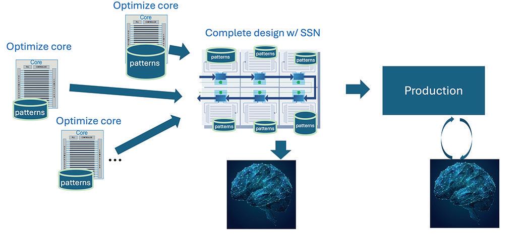
Core DFT & patterns complete as soon as core is ready (no iterations)
optimized for the current pattern sets. In addition, cores are designed and developed at varying times in the design flow and an overall solution would need to be fed back to adjust each core DFT structure as the newer cores are finalized. This traditional hierarchical methodology unable to keep up with the fast design cycles and high complexity scaling currently seen in the industry. Therefore, the overall hierarchical DFT methodology is too static and needed dramatic innovation.
We introduced a novel method to remove most of the variables that needed to be optimized during hierarchical DFT architecture planning. It uses packetized scan data delivery. This had a dramatic reduction in DFT architecture planning and test time, with the side benefit of improvements in power during test, timing closure, and identical core scaling[4]. The solution is completely flexible as opposed to distributing top level IO pin bandwidth between cores. It can optimize any number of IO pins to any number of core channel requirements and pattern sets. The packetized solution can adjust to any changes in core IO requirements or pattern sizes in
SSN optimizes any patterns an cores (at any time)
software alone.
The innovation is to use any size SoC level IO pins as a high-speed packetized bus. Each core is programmed to know when to pull its necessary data off the bus and independently apply it to the core’s scan logic. Thus, any size bus, even onebit can be used to load data for any size core scan channels whether it is one bit or 64 bits. This not only enables cores of different scan channel IO requirements to share the same bus, but also dramatically improves timing closure since each core independently shifts and captures. As a result of shifting the DFT design to a packetized data delivery, the core DFT is independent of its SoC embedding and other core demands. Therefore, complex tradeoffs between SoC IO pins and core requirements are no longer needed. With a packetized data delivery structure, static groups of cores do not need to be pre-defined. It is flexible such that any set of cores or any original or new test patterns can be programmed into the packets at any time. This replaces pre-defining the optimization for a given hierarchical DFT structure prior to design completion. By using packetized delivery software, optimization can occur at any time without changing the design. We refer to this flexibility and automation
Can optimize for different patterns/cores based on production results
as adaptive intelligence using analytical AI as there is no training involved. This analytical AI provides a solution to a very complex optimization challenge. Industrial results report a 10x improvement in productivity and significant test time reduction using this packetized scan delivery method [4] compared to previous methods.
The second workflow uses test patterns generated in the first workflow and applies them to fabricated devices using automatic test equipment (ATE). High volume manufacturing is a nice application of machine learning to highlight systematic defect causes and improve yield since there is a large amount of data available. There are thousands of devices that get tested in production today, each with a large number of test patterns uniquely applied to each device. Furthermore, for each test pattern there are millions of sampled data points with passing and failing scan cell captures. In this workflow, we use unsupervised machine learning on this big data set to improve yield.
A basic workflow for scan diagnosis is shown in Figure 3. Scan diagnosis uses passing and failing production test patterns to explain which physical defects might be
Physical location
Logic location

causing mismatches captured on the ATE. However, the diagnosis report for a single die can still contain a list of 10s to 100s of defect suspects, which can all explain the failing behavior. However, only one of these suspects is actually causing the device to fail. Viewing the data from just one die in isolation, we can’t narrow down this list of defect suspects to the most probably cause. The following solution enables tracking the failures back to the root cause by examining the failures over large qualities of parts.
In volume manufacturing, there are thousands of devices failing in a day. Based on historical experience we assume there are just a handful of defect mechanisms that are causing most of the failures. This enable us to perform a joint probabilistic analysis over all the failing device reports and use the power of machine learning (ML) to further narrow down the list of defects for each failing device. By applying this ML algorithm, referred to as Root Cause Deconvolution (RCD) [5][7], on all the failing devices, we obtain a Pareto. The Pareto informs us about the yield fallout due to each type of defect mechanism. The benefit of this approach is that we do not need anyone telling us the actual defect mechanism for any of the failing devices. RCD is therefore an example of
unsupervised ML, since it doesn’t need any labelled data to operate.
Scan diagnosis can be considered a digital twin of failure analysis (FA). Using only software instead of physical equipment it quickly works out an explanation and root cause for a physical defect in a device. Scan diagnosis enables us to perform a virtual FA on every failing device. Unlike many other methods, we do not consider a suspect in a diagnosis report independent of the other suspects in the report. We consider all the suspected defects together.
It is important to consider what set of diagnosis reports are used for the RCD ML process. The sample set of scan diagnosis reports for RCD needs to have a perceived root cause commonality. For example, it wouldn’t make sense to process wafer scan failures from completely different technology nodes.
Once the root causes have been determined by the AI system, a small number of directed FA can be undertaken, to identify the underlying physical defect mechanisms. As a result of RCD, we can eliminate most of the suspects from a diagnosis report, thereby significantly improving the resolution of a diagnosis report [6] .
The location pinpointed by RCD is typically very small and there is usually no need to do fault isolation before doing FA. This dramatically speeds up FA. Unfortu-
nately, for the latest technology nodes, we can no longer use techniques such as laser voltage imaging / laser probing.
Cell-aware test is a method of modeling physical defects within process technology cells to ensure that all possible potential defects were targeted and detected by ATPG. Cell-aware diagnosis (CAD) takes production failure results and reverse maps it against the cell-aware models to understand and identify potential failure root causes within the cell. RCAD is an extension of RCD to within the cell. This helps identify the problematic root causes within a standard cell [2]
Applying machine learning on scan diagnosis reports for yield improvement has been taking place for over a decade. This is a very practical application of machine learning and results show a 2x improvement in diagnosis resolution [6] .
AI has been a useful aid in EDA software for many years. However, instead of blindly applying AI it is best to combine domain knowledge with AI for effective solutions. For example, packetized scan data network removes many dependencies and variables, greatly simplifying the DFT architecture and planning. The task of optimization was shifted from tedious engineering planning to rapid AI software automation within a flexible DFT archi-
tecture. The results with this method are dramatic and it has quickly become the standard approach for advanced SoCs.
At the same time unsupervised machine learning techniques can be applied to vast amounts of scan failure data. The RCD system quantifies all failures to determine the root causes and significantly improves yield. It also dramatically improves the resolution for individual diagnosis reports.
Over the next few years, we see additional applications of AI in the areas of DFT, test, and production. Basic use cases include expert systems and copilot types of
features which will lead a user to solutions quicker. In addition, training-based systems employed locally within a company will learn the specifics of a company’s design and ATPG trends. This will improve results on future DFT and ATPG. ◆
References
[1] R. Press, F. Aylstock, L. Charles, L. Elerin and J. Hintz, “The application of neural network technology to built-in test false alarm filtering,” in American Institute of Aeronautics and Astronautics, Inc, 1993.
[2] M. Sharma and Y. Pan, “Machine Learning Inside the Cell to Solve Complex FinFET Defect Mechanisms with Volume Scan Diagnosis,” Elec-
tronic Device Failure Analysis, vol. 21, pp. 4-9, 2019.
[3] J. Remmers, M. Villalba and R. Fisette, “Hierarchical DFT Methodology - A Case Study,” in Intl Test Conf. (ITC), 2004, 2004.
[4] J.-F. Côté, M. Kassab, W. Janiszewski, R. Rodrigues, R. Meier, B. Kaczmarek, P. Orlando, G. Eide, J. Rajski, G. Colon-Bonet, N. Mysore, Y. Yin and P. Pant, “Streaming Scan Network (SSN): An Efficient Packetized Data Network for Testing of Complex SoCs,” in 2020 IEEE International Test Conference (ITC), 2020.
[5] B. Benware, C. Schuermyer, M. Sharma and T. Herrmann, “Determining a Failure Root Cause Distribution From a Population of Layout-Aware Scan Diagnosis Results,” IEEE Design & Test of Computers, 2012.

Jason Blocklove
ECE Ph.D. Candidate at NYU
Digital hardware design has primarily been performed by hardware design engineers with specific and niche skill-sets write their designs in hardware description languages (HDLs), such as Verilog or VHDL. While other methodologies have emerged over time, such as highlevel synthesis (HLS), they often have significant drawbacks and are primarily used for only specific applications. The digital design pipeline, as such, has continued to rely on a significant amount of manual effort on the part of the hardware design engineer, even for creating conceptually simple designs. With the advent and mainstream adoption of generative artificial intelligence (AI) large language models (LLMs) in recent years, a new design path has been made available, by which hardware designers can leverage these new technologies to drastically improve their productivity and offload some design and HDL-writing tasks to LLMs.
The process of designing hardware has consistently been a very manual process, requiring engineers with niche skills to architect designs, write hardware description language (HDL), synthesize, implement, and ultimately fabricate a new device. With the creation and widespread use of large language models (LLMs), there are now new ways to potentially simplify some of these tasks. LLMs have, from their inception, been used to generate software code, but HDL has idiosyncrasies that must be accounted for. To this end, over the last several years much work has been done to determine how capable LLMs can be in the digital design workflow. This paper will detail and analyze the steps taken so far in the journey to making the process of
digital hardware design more accessible with generative AI.
The first LLM specifically fine-tuned for Verilog was produced by Pearce et. al., and called DAVE, a pre-trained GPT-2 model for translating natural language into functional Verilog [1] It was trained over a custom, though small, dataset of “Task/Result” pairs, similar to simple textbook-style problems that would be commonly asked of undergraduate digital logic design students. The fine-tuning dataset for DAVE was broken into three categories of task: prescriptive tasks, which only require a simple translation; descriptive tasks, which are more complicated and describe a complete functionality without detailing how it should be implemented; and multi-tasks, which are concatenations of two to four register or assignment templates. A selection of these tasks were set aside from the training set for validation and evaluation.
DAVE performed, on average, quite well. It was able to generate the correct answer in 94.8% of all validation tasks. However, this initial work has significant limitations, primarily in its ability to be “creative” in its responses. Further, the tasks used for training and testing were intentionally simplistic, given the abilities of LLMs at the time. Many of these shortcomings have been addressed in the works since.
Following the success of DAVE and the further increasing use of LLMs in dayto-day activities with the introduction of tools like GitHub’s Copilot, Shakur et. al. sought to improve upon the concept by fine-tuning newer models over a more
significant corpus of data [2]. This new set of models, VeriGen, was fine-tuned using a corpus of both Verilog examples from GitHub, and text from 70 Verilog-based textbooks. The models used included three versions of CodeGen, each with different numbers of parameters, as well as Megatron-LM and J1-Large.
The VeriGen models were then evaluated using two unique problem sets. The first is composed of 17 Verilog problems, once again primarily based on undergraduate classroom exercises. These include problems ranging from simple assignments and basic gates to arithmetic circuits and somewhat abstract state machines. After these initial tests, the models were further evaluated using a significant number of problems from the Verilog training website HDLBits [3], an effort that future works will continue to expand upon.
The VeriGen models, especially the fine-tuned CodeGen model with 16B parameters, showed significantly better results than the non-fine-tuned state of the art models at the time, even performing at or better than GPT-3.5-Turbo and achieving nearly the same performance as the newly released, at the time, GPT-4.
More recently, as fine-tuning has become more accessible and LLMs have become more widespread, an increasing number of models specifically for hardware design have been developed, both open-sourced and commercially. Commercial efforts have come with models like PrimisAI’s RapidGPT, Cadence’s JedAI, Nvidia’s ChipNeMo, all of which have their own methods of generating hardware designs. Further, there are even some models, like ChatEDA, that aim to use LLMs to automate the tooling for chip design.
RTLCoder joins DAVE and VeriGen
as an open-source fine-tuned model for generating Verilog [4]. RTLCoder made use of an automatic training dataset generation, which was able to create a significant corpus over data with over 27,000 labeled training samples. This corpus was used to fine-tune some more recent LLMs, specifically a Mistral and a DeepSeek model. Reported results show that these new models outperform even GPT-4 on a set of benchmarks from HDLBits, provided by VerilogEval [5]
Evaluating the performance of LLMs to design hardware has been a sticking point for many of the works up to this point. Each paper proposed its own set of tests for benchmarking the LLMs being used, often deriving them from textbook questions or previously offered exercises in undergraduate classes. While this was sufficient for a time, as the amount of work in this area increased, so too did the need to be able to compare results across different efforts. Several works have since proposed standard test sets for benchmarking. RTLLM provides an open-source repository of 30 designs intended to evaluate an LLM’s ability to generate Verilog [6]. These benchmarks are separated into “Arithmetic” and “Logic” benchmarks, including things like specific multiplier architectures, state machines, and even a simplified RISC-V CPU. Along with the design specifications which are given to the LLMs, RTLLM also gives complete testbenches for each design to be able to verify the functionality.
Similarly, VerilogEval provides a benchmarking set with the same goal, though it uses prompts and testbenches from HDLBits, similar to those originally used in VeriGen, though standardized with help from the creator of HDLBits. VerilogEval gives two separate benchmark sets with differing prompts made for the same designs, providing some extra insight into how prompting can affect the generated designs. In total, the benchmarking sets include 143 and 156 tests respectively.

With the release and common adoption of conversational LLMs, such as ChatGPT, a new question had to be asked: “Can these LLMs be used to write and fix Verilog like an engineer?” Hardware engineers very often have to hunt down and fix bugs in designs using the feedback from tools and the outputs of design simulations. Can these commercial LLMs now do the same thing? Moreover, can they be used in conjunction with an experienced engineer to define and create a novel design?
To attempt to answer this question, Chip-Chat was made: a work in which an experienced hardware engineer worked with ChatGPT-4 to design and develop a novel resource-constrained 8-bit microprocessor architecture [7]. This was done in an unscripted manner so that the designer could ask questions of and make suggestions to ChatGPT as if it were another engineer. This process led to ChatGPT defining and then implementing a completely new instruction set architecture for an accumulator-based processor. The implementation was done completely by ChatGPT, with the engineer only able to provide feedback on things that would or would not work. Once complete, the processor was taped out as part of Tiny Tapeout 3, in the first
tapeout of completely AI-written hardware. Once the hardware was received it was verified that the design works as expected.
Feedback from an engineer in the manner of Chip-Chat can be nebulous and expensive, though. To begin to address this, a more standardized process of providing this feedback was proposed, detailed in Figure 1 [8] The flow chart provided a standard method by which an engineer could interact with the LLMs to try to prompt for a complete Verilog design and a matching testbench. With the aim of also taping out a set of benchmark circuits on Tiny Tapeout 3, a set of 8 benchmarks was chosen with constrained IO to match the requirements of that iteration of the tapeout. These benchmarks were once again derived from exercises given to undergraduate students, ranging from a simple shift register to a simulated dice roller. To generate the designs, first a base design and testbench was requested, then compiled and simulated with Icarus Verilog (iverilog) to get feedback on the design’s success. That feedback was given back to the LLM in the same conversation and a fix was requested. Should just feedback from the tool not be enough to solve the issue after multiple attempts, feedback from an engineer with varying levels of complexity was provided, following the order of the flowchart.

Ultimately, of the models available at the time, ChatGPT-4 performed the best, completing 12 of the 24 tests with no human feedback necessary. The first test set performed was successfully taped out and the hardware has since been verified to be functioning as expected. However, there were still some notable concerns: that the testbenches generated often had poor test coverage so that even when they passed the design it was not necessarily guaranteed to work, and that generating correct HDL still often had to rely on human feedback which, though more structured than before, still suffers from concerns of cost and repeatability.
To remove the difficult-to-control variable of human feedback from the process
of hardware generation, a tool called AutoChip was developed, which sought to leverage only feedback from tools and testbenches to iteratively correct errors in LLM-generated Verilog, as well as leverage multiple LLMs on a single problem. Figure 2 shows the tool flow, where a design is given to a “small” LLM to generate Verilog, it is evaluated using a compilation tool and provided testbench, any output from the tools is added in to a new prompt and that is given to an LLM again, selecting a “big” LLM for the final iteration.
AutoChip was evaluated using a set of 120 problems from HDLBits, similar to the set of benchmarks proposed in VerilogEval. Four “small” LLMs were tested, with the one evaluated “big” LLM being GPT-4 which was the state of the art at the time. Multiple feedback
strategies were also evaluated, termed “succinct” and “full” feedback: succinct feedback kept only the most recent errors needing correction, while full feedback kept the whole conversation when prompting for corrections. Succinct feedback was tested more thoroughly, as in initial verification tests it showed better performance at the cost of fewer tokens. Table 1 shows the results of evaluating AutoChip with several different configurations of LLM, number of tests done, and maximum number of iterations, finding that GPT-3.5-Turbo followed by one iteration of GPT-4 produced the best results, with 87.15% of tests fully passing.
Figure 3 sheds some further light on these results, showing that while GPT3.5-Turbo performed well on simpler tasks, more complex circuits caused significant issues. With a single iteration of GPT-4 following the attempts by GPT-3.5-Turbo, notably more tests were completed successfully.
Large language models have, in just the last few years, shown themselves to be extremely capable tools for improving productivity in many sectors. As such, researchers have been trying to determine how best they can be used for hardware


design from fine-tuning to frameworks for improving commercial model performance. Ultimately, current results show that while they are promising tools and can be used quite effectively as force-multipliers for experienced engineers, they still fall short of being able to create new complex designs without a significant amount of handholding by an experienced design engineer. ◆
References
[1] H. Pearce, B. Tan, and R. Karri, “DAVE: Deriving Automatically Verilog from English,” in Proceedings of the 2020 ACM/IEEE Workshop on Machine Learning for CAD, Virtual Event Iceland: ACM, Nov. 2020, pp. 27–32. doi: 10.1145/3380446.3430634.
[2] S. Thakur et al., “VeriGen: A Large Language Model for Verilog Code Generation,” ACM Trans Autom Electron Syst, vol. 29, no. 3, p. 46:1-46:31, Apr. 2024, doi: 10.1145/3643681.
[3] H. Wong, “HDLBits Problem Sets.” Accessed: Sep. 23, 2022. [Online]. Available: https://hdlbits.01xz.net/wiki/Problem_sets
[4] S. Liu, W. Fang, Y. Lu, Q. Zhang, H. Zhang, and Z. Xie, “RTLCoder: Outperforming GPT-3.5 in Design RTL Generation with Our Open-Source Dataset and Lightweight Solution,” Feb. 20, 2024, arXiv: arXiv:2312.08617. doi: 10.48550/ arXiv.2312.08617.
[5] M. Liu, N. Pinckney, B. Khailany, and H. Ren, “VerilogEval: Evaluating Large Language Models for Verilog Code Generation,” Sep. 14, 2023, arXiv: arXiv:2309.07544. doi: 10.48550/ arXiv.2309.07544.
[6] Y. Lu, S. Liu, Q. Zhang, and Z. Xie, “RTLLM: An Open-Source Benchmark for Design RTL Generation with Large Language Model,” Nov. 11, 2023, arXiv: arXiv:2308.05345. doi: 10.48550/ arXiv.2308.05345.
[7] J. Blocklove, S. Garg, R. Karri, and H. Pearce, “Chip-Chat: Challenges and Opportunities in Conversational Hardware Design,” in 2023 ACM/IEEE 5th Workshop on Machine Learning for CAD (MLCAD), Sep. 2023, pp. 1–6. doi: 10.1109/MLCAD58807.2023.10299874.
[8] J. Blocklove, S. Garg, R. Karri, and H. Pearce, “Evaluating LLMs for Hard-
ware Design and Test,” Apr. 23, 2024, arXiv: arXiv:2405.02326. doi: 10.48550/ arXiv.2405.02326.
Jason Blocklove is an Electrical and Computer Engineering Ph.D. candidate at New York University, studying under Dr. Ramesh Karri. His research focuses on additive manufacturing security, leveraging generative AI models for hardware design, and security analysis of AI models for generating hardware.
R&D Test Engineer
Broadcom
Owing to a very diverse and accomplished association of MEPTEC members, there are many informative, instructional, and entertaining stories to be told. “Catching Up With...” will feature stories from and about our members.
Phil Nigh (https://www.linkedin.com/ in/phil-nigh-801b719/) is a prominent figure in the test industry and he currently is a R&D Test Engineer at Broadcom. This interview was conducted via email and edited for clarity.
How did get into the Sciences?
I first became interested in Math in high school thanks to my high school math teacher, Chris Leuthold, who I remember fondly. Really engaging in Math in high school started the development of my problem-solving capability. Professor Wojciech Maly, my Carnegie Mellon University PhD advisor, described the benefit of a Math degree a few years later to me and my son: Math teaches you how to think in a logical way. And there are many different professions where you can take advantage of that skill developed with a Math degree.
After earning your Bachelor of Science and Master of Science degrees, where did you head?
I started my career at IBM (over 40 years ago) where my first project was working on mainframe products that had packaged parts with 90-120 chips each. My role was to come up with new tests that would detect defective chips as these chips failed in the system for some reason. However, they had initially passed and would come back and continue to pass all of our production chip tests. I’m sure IBM had low expectations – but we were able to come
up with new tests that would fail most of the defective chips. The failures we found were physical defects, but the behavior was subtle. We were one of the first teams to generate delay fault tests (not just stuckat) and we used methods like adaptive diagnostic methods and circuit defect characterization. This was great work with colleagues like Jim Monzel, David Wu, and many others.
Even though this work was several decades ago, it sounds like many challenges the industry is currently facing.
My career has really gone full circle! It is true that my latest project is similar to the one I worked on as a young engineer at IBM. At Broadcom, we work with our key artificial intelligence (AI) systems customers to develop new test methods to reduce their system test fallout and field failures. Some of the products include multi-die advanced packaging with tens of dies in one package. One of our big challenges today is Silent Data Corruption (SDC) failures. Working with Kamal Jasti, we’ve been able to develop new tests that detect over 50% of the system/field failures. And we’re working hard on the other 50%! Most of the methods implemented were not the typical approach expected but were the results of exploring the behavior of these chips as failures often behave the opposite of defect-free chips.
Obviously, you did a lot of interesting work between that first project and today. How did your career progress?
After working an initial three year stint at IBM, I went back to graduate school in the Electrical & Computer Engineering department at Carnegie Mellon with Professor Wojciech Maly. I studied how

defects behave and methods to detect them and diagnose the failure location. Although my PhD dissertation was specific to designing circuits to detect subtle defects through current measurements, our research project was mainly to understand defective circuit behavior and detection methods. This was an excellent opportunity to focus on a specific project for years and thoroughly understand the complex behavior of subtle defects. Some of the methods we developed in the 1980s are so fundamental they are still relevant to SDCtype failures today.
How did your collaboration in and between both industry and academia start?
It was interesting and useful to start interacting with some of the industry leaders while I was at CMU. This interaction continued beyond CMU with industry projects in the following few years. One of the things I learned is that I liked collaborating with others in industry and academia. I found many people who were smart and interesting. And who were willing to work together to learn from each other! I enjoyed debating the big industry challenges with experts both from both industry & academia.
One particular project we drove through the SEMATECH consortium, with about six companies in the industry and three academic researchers, where we applied a number of different test methods to a large sample of chips. We collected a ton of data from thousands of chips and shared all the results among these companies. We also shared all the raw data with over 25 academic researchers. The researchers then used this data to help drive graduate research with their students. I learned a lot from all the discussions with these industry and academic colleagues.

You worked at IBM for almost 35 years. Are there any collaborations that stand out?
One unique product requirement was that IBM mainframes could never fail, especially for the Z-Series. IBM took this very seriously and the number of field failures was virtually zero. It was a good challenge to contribute to achieving this level of quality and reliability. Most of our systems would have zero failures per year and these were large systems with 1,000s of chips. I learned a lot from distinguished IBMers like Franco Motika, Jody Van Horn, and John Harris. For many years within IBM, we had the advantage of having complete end-to-end quality data from the wafer fab through the end system products. It allowed learning and optimization that would simply not have been possible if each system component were from different companies.
You are also well known for your “rump” sessions at industry test events. Some say they are the best (unofficial) part of the event. Would you tell us more about these?
One of the projects that I’ve liked working on is setting up the “Industry Test Challenges” workshop. Around 1998, we started to setup technical discussions meetings around the International Test Conference and the VLSI Test Symposium. We still do this once a year typically at one of these two events. Industry
experts are invited to present “case study” presentations of the problems that they are working on. Then we encourage back-and-forth discussion during these presentations. The purpose is to discuss leading edge problems and the goal is to have everyone learn from it. I’ve found that people are more than willing to share their experience if they can get something out of it and they see that others also are willing to share. These meetings help the industry learn from some of the experts in attendance. And I’ve learned many useful things from those meetings over the years! There is no cost to attend and we always get more than 100 attendees. I have also setup many smaller, closed meetings where a few key industry people gather to share our experiences. Especially on topics that are not discussed in normal conferences and workshops. These are mainly focused on problems we were having at the time. Some of my best friends in the industry have participated and we jointly have learned a lot over the years. An extra special thanks to Bob Madge, Ken Butler, David O’Brien, Brady Benware, and many others!
In addition to IBM, you worked at GLOBALFOUNDRIES and now Broadcom. All rather different companies and culture. What has Broadcom been like?
I’ve worked at Broadcom for the last five years. It is really interesting to work on some of the most relevant products in the industry – AI processors. It has been crazy at how these products have taken off. Broadcom is a company where decisions are made much more quickly and

without endless debate. That is refreshing and has allowed us to drive quality and test improvements much more quickly than at my past companies.
Driving (new) strategic directions is always one of the most interesting projects. The emergence of Heterogeneous Integration (multi-chip products, chiplets, 2.5D 3D products) significantly changes many of the approaches to test, quality, supply chain, and yield. The best approaches aren’t always clear and the best methods can be different from company-to-company. Our goal should be to enable the industry to use these technologies and ensure that those challenges don’t slow us down.
Working on improvements to product quality and being able to detect Silent Data Corruption failures before they happen has been rewarding. I used to do a talk where I said a role of a Test Engineer was to “predict the future.” We were supposed to identify the chips most likely to fail in the field. And find them during production testing before they were shipped, even though they passed all normal production tests... That is the same challenge today as it was 30 years ago.
My family moved from Vermont to Colorado for me to join Broadcom. We loved Vermont! Summers are great. We have met quite a few people who have moved between Vermont and Colorado – in both directions. However, the golf courses are closed five months of the year in Vermont giving a clear advantage to Colorado.
My favorite hobbies are family time (with my wife Celeste, my son Chris, and my daughter Rachel), travel, puppies ... and sports (mainly golf as I got older). We’ve been very lucky to take a number of great vacations. Our next one may be to Portugal or Argentina. Perhaps to scope out retirement in the not-too-distant future. ◆

SMART MICROSYSTEMS is excited to reside in America’s Silicon Heartland as the Midwest region of the US is now poised to create the next international semiconductor boom. As part of the semiconductor supply chain, SMART Microsystems provides services for microelectronic sub-assembly manufacturing. In addition to process development expertise, SMART Microsystems has in-house Test & Inspection capabilities making it a comprehensive resource for the development and manufacture of the next generation of products that require microelectronic sub-assemblies. Call 440-366-4203 or send us an email at info@smartmicrosystems.com for more information.

Microelectronic Sub-Assembly Manufacturing. 141 Innovation Drive, Elyria, Ohio 44035