9 minute read
Vertically-integrated Packaging Solutions Driven by Innovative Applications
from MEPTEC REPORT WINTER 2022
by MEPTEC
Mark Gerber, Lihong Cao, Vikas Gupta, Patricia MacLeod ASE, Inc.
Editor’s Note: This article is based upon an article originally published in Chip Scale Review (July/August 2022)
THE INCREASE IN TRANSISTOR density continues to challenge foundry companies and integrated device manufacturers (IDM) companies. This is driven by the need for improved performance and higher fab yields, which have led companies to investigate heterogeneously integrated (HI) advanced packaging solutions. Advanced silicon node yield attainment is a key driver for looking at ways to approach intellectual property (IP) block integration and has opened up new creativity on how to bring the SOC building blocks together in a disaggregated format. The advanced silicon high development cost and lower yields are challenging designers to look for new ways of disaggregating system on chips (SoCs), to reduce the die size, by separating IP blocks that may not need to be in the most advanced silicon node. Creating a SoC-like solution with optimized silicon nodes for different portions of the chip is a new key focus. Advanced redistribution layer (RDL) packaging technologies that add a vertical integration element allow for a denser, 3D approach. At the same time, the traditional packaging components, such as substrates and interconnect technologies are also being pushed to limits in which new solutions are needed to extend roadmap requirements. These roadmap requirements are seen across all industry market segments including server, networking, graphics, mobile and telecom infrastructure.
Each market segment has unique requirements to meet their product needs and there are a few common challenges across all these segments. For example, as advanced silicon nodes continue to shrink the die size and increase the power density per square mm, the challenge of signal noise increases dramatically and must be addressed. New ways of providing power into critical areas of the IP block and system design also create power delivery challenges. In addition, the impedance challenges of connecting one chip to another in a system dramatically reduces the performance that can affect battery life, or power requirements in an array bank of processors. The higher density per area of transistors and reduced line width to carry power also challenge the thermal capabilities of the package—and when combined with other areas of impedance in the system, can create larger system-level problems.
These challenges are impacting traditional SOC layout and architecture plans and require a new set of package structures. ASE has developed a series of RDL-based vertically-integrated packaging solutions that continue to evolve to meet these various challenges. These include six pillars underneath the VIPackTM platform include: fan-out system-in-package (FOSiP), fan-out chip-onsubstrate (FOCoS), fan-out chip-on-substrate bridge (FOCoS-B) (embedded), fan-out package-on-package (FO-PoP), 2.5D/3D and co-packaged optics (CPO). Each one of these package pillars addresses specific performance and/or form fit challenges and provides advanced solutions that address the market segments listed above. Packaging innovation within these six technology pillars are being evolved by ASE and these will be reviewed in the sections below.
FOSiP
As more companies look to system-level solutions and integration, system-in-package technology has expanded to leverage some more advanced process tools. The term system-in-package (SiP) has had many definitions over the years and as its umbrella has grown across both the low-end and high-end application spaces, the description must allow for advancements. ASE published its formal definition in 2014, which states that a SiP module is a package that contains an electronic system or sub-system and is min- iaturized through IC assembly technologies. Although this is a broad definition, it still holds true today, as individual silicon solutions are moving toward highly-integrated system or sub-system level solutions.
If we look at the various package platform roadmaps today, we see a trend around miniaturization, not just for final package size, but also for performance. For the mobile space, the original equipment manufacturer (OEM) suppliers are driving component size reduction or integration across all sub-modules to enable more room for new functionality while managing battery space.
FOCoS
The integration of both a substrate-based package technology, with an RDL intermediate routing integration, has enabled a new structure called FOCoS. This package pillar helps to address the limitations of traditional flip-chip packages where a single SoC is assembled on a substrate. Two distinct categories are:
1. Utilizing the fan-out RDL process to redistribute the die-level I/Os to a coarser bump pitch to utilize less aggressive substrate design rules and/or to reduce the number of layers on the substrate. This approach also helps with low-k reliability issues related to chip-package interactions.
2. Multi-die and chiplet integration where two or more dies can be reconstituted into a fan-out module and then assembled on a substrate. The FOCoS platform provides versatility in integrating multiple instances of same dies or different dies across digital/analog and other functionalities to provide a highly integrated heterogeneous solution. Chiplet integration offers a compelling value proposition for yield improvement, IP reuse, performance, and cost optimization. Heterogeneous integration through advanced packaging technology enables chiplet integration with separate designs and different manufacturing process nodes within a single package. It has provided advancement for more intelligence, greater connectivity, and higher performance at a more manageable cost.
Advanced packaging technologies such as flip-chip ball grid array (FCBGA), multi- chip modules (MCMs), and 2.5D Si throughsilicon vias (TSVs) have been widely used for chiplets and die-to-die (D2D) interconnections across various semiconductor segments. However, with increasing demands for high density, high speed and low latency of D2D interconnects, the FC MCM package has reached its limit due to the large Cu interconnect line/space L/S > 5/5 μm in the substrate, and unsustainable costs related to 2.5D Si TSV with larger interposer size (>2X reticle size). Therefore, alternative packaging solutions such as 2.5D TSVless and fan-out RDL interposer have been developed in recent years. Three of the six VIPackTM technology pillars namely, FOCoS, FOCoS-Bridge and 2.5D/3D provide chiplet integration options depending on the bandwidth, latency, and other design/performance requirements.
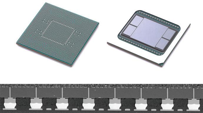
There are a number of FOCoS solutions, e.g., FOCoS chip first (FOCoS-CF) and FOCoS chip last (FOCoS-CL), that have been introduced. The schematic structure of FOCoS is shown in Figure 3 with the cross-section image as shown in Figure 4. The FOCoS package contains different chips and flip-chip devices mounted on a high pin count BGA substrate, and Cu RDL replaces the expense of using a Si TSV interposer to provide interconnects.
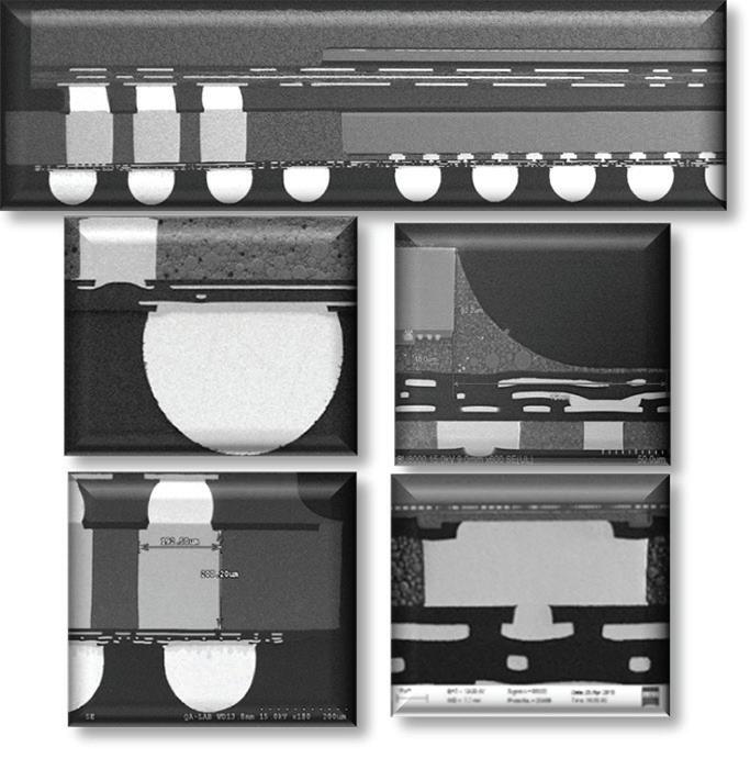
The FOCoS packaging technology has enabled chiplets integration with multiple RDL interconnects up to five layers, a smaller RDL L/S of 1.5/1.5 µm and a large fan-out module size of 32x38 mm2. It also provides a wide portfolio integration, such as an application-specific integrated circuit (ASIC) with high-bandwidth memory (HBM) and ASIC with Serdes across many segments of HPC, networking, artificial intelligence/ machine learning (AI/ML) and the Cloud. Furthermore, FOCoS has demonstrated the better electrical performance and lower cost than 2.5D Si TSV because of the elimination of the Si interposer along with reducing parasitic capacitance.
FOPoP
The Mobile phone space has continued to drive new functionality that has evolved the component level integration as well as the individual package requirements. The trend for most handheld consumer devices development has been towards multi-functional, high-definition display, low power consumption, high performance, and thin/ light packages, that are now commonly found in smartphones, tablets, and wearables. This trend drove the development of complex 3D or 2.XD integration on integrated circuit (IC) packages. Flip-chip package-on-package (FCPoP), initially with traditional C4 solder bump and later with fine-pitch Cu pillar was the primary package used because of the inherent low-inductance package interconnect.
The ever-increasing need for higher performance and thinner form factor drove the accelerated implementation of FOPoP in the mobile processor application space. The fundamental high-density, substrate-less configuration of the FOPoP package results in higher package performance because of the elimination of the substrate parasitic inductance along with a thinner package form factor.
Overall, the FOPoP structure provides 1) higher interconnection density and integration through a finer L/S redistribution layer (RDL) as compared to substrates, and 2) a shorter interconnect length resulting in better electrical performance, and 3) a smaller/thinner form factor because the fan-out technology allows die I/O signals to be fanned-out to a region larger than the die area without an organic substrate to meet a higher I/O count.
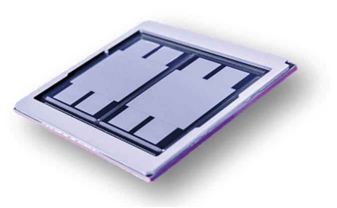
Figure 1 shows a FOPoP package with the cross-section image showing the die, RDLs, and Cu post details. Additional cross-section details are included in Figure 2, where the active side of the die utilizes two routing planes to fan out the I/O signals. Fine-pitch Cu posts are used on the periphery to enable electrical connections for the package on top.
The FOPoP package platform is further enhanced for increasing complexity and high-performance needs by enabling RDL on both sides of the die for increased integration and functionality. Furthermore, both landside caps and near-die deep trench capacitors (DTC) can be implemented to meet the power integrity requirements of advanced nodes. FOPoP is, and will continue to be, a key package platform for application processors, mobile/auto antenna-in-package (AiP), and co-packaged silicon-photonics applications.
FOCoS-Bridge
Consumers with phone storage limitations and companies like Google and Facebook continue to add content to their data storage and cloud accounts. The increasing amount of data from all sectors, driven by digital transformation, is raising a problem of operational and storage costs. Meanwhile, the exponential cost leaps of silicon scaling and the unaffordable increasing of Si die size over the reticle limit have created an inflection point for the semiconductor industry. FOCoS-CF and FOCoS-CL technologies have been developed and introduced by using RDL interconnect for chiplets integration at
ASE. FOCoS-CF has been in mass production since 2016. Because of the inherent fanout RDL process limitation, however, it has hit a bottleneck in the manufacture of RDLs with higher layer counts (>6 layers) and finer line/space dimensions (L/S < 1 µm / 1 µm) for the applications that require high-density D2D connections, high input/output (I/O) counts, and high-speed signal transmission.
To address this, a new technology named as
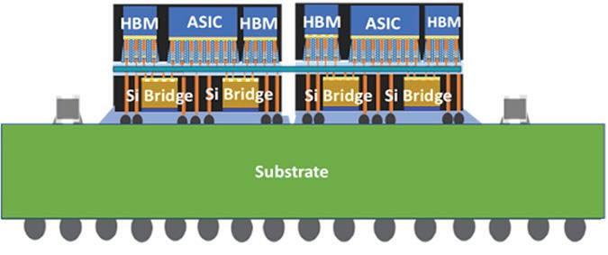
FOCoS embedded Si bridge (FOCoS-B) has been developed to enable ultra-high density D2D interconnection with L/S < 1/1 µm for high-density chiplets integration. FOCoS-B packaging technology enables D2D interconnect by embedded a small Si die in a fan-out RDL interposer. The small Si die plays an interconnection bridge role between chiplets with L/S < 0.8 µm / 0.8 µm. Figure 5 shows the schematic structure of a FOCoS-B pack- age with the optical image. It is composed of two identical fan-out modules, which are assembled on one FCBGA substrate in an MCM arrangement. The fan-out module is integrated by 10 chiplets (two ASICs and 8 HBM2e with 8 Si bridge dies). The FOCoS-B package body size is 78x70 mm2 with two fan-out chip modules at a size of 47x31 mm2, respectively. FOCoSB packages have passed reliability tests and chiplets integration has achieved good integrity. Figure 6 shows the cross-section of a FOCoS-B package; this package has extensive options and flexibility for multiple bridge die integration for mobile products, HPC, AI/ML and server applications.

FOCoS technology has demonstrated better electrical performance for chiplets integration. The fine-pitch RDL in FOCoS is essential to provide lower insertion loss and better signal integrity (SI) because of the thicker Cu RDL with L/S=2/2 µm compared to a thinner Cu RDL with L/ S=0.8/0.8 µm in a 2.5D Si TSV interposer, which results in the lower parasitic capacitance and lower cross talk. Figure 7 shows the insertion loss comparison between FOCoS and 2.5D Si TSV at different frequencies. The better eye diagram performance is also observed in FOCoS compared to 2.5D SI TSV, which is shown in Figure 8.
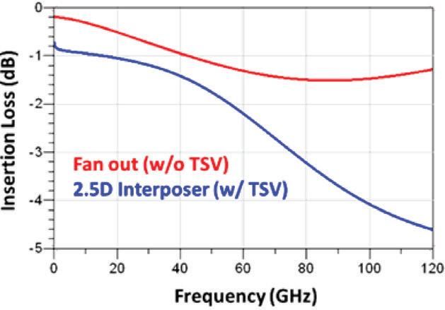
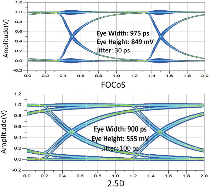
Table 1 by TSR in February 2022 shows the modular adoption rate across various radio frequency (RF) modules. The one reduced adoption is partially due to the exit of LG, shrinkage of Huawei and adoption of the power amplifier module with integrated duplexer (PAMiD). Because of this trend, the need for technology that enables further miniaturization and integration while managing new performance challenges is driving companies to look at fan-out wafer-level packaging (FOWLP)

RDL SiP-based technology. Wi-Fi and ultra-wide band (UWB) RF modules are also leveraging the SiP platform. Figure 9 shows an example of a UWB module in an Apple iPhone 13 Pro with traditional SiP integration tools including packaged IC, discrete and IC components (five die, FC, WLP and shielding).
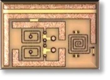
Specific drivers for FOSiP consideration include substrate thickness reduction, line/space control to minimize RF variation, and tighter component spacing for reduced losses for improved battery life (Figure 10). As with most advanced technologies, the key challenge is how to manage cost. When considering SiP, there is the tendency to focus on raw single-package cost vs. the system cost that integrates multiple packages and components. An overall system size reduction is realized by reduced individual component packaging, doublesided RDL for dense component integration (< 50 µm spacing) and a second RDL stack plane can simplify test, and in some cases, eliminating the substrate can help to enable a more competitive system solution.
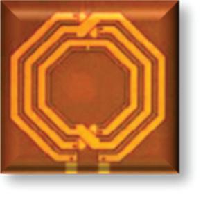
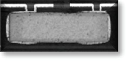
Some of the key tools to consider in a fan-out RDL-based SiP may include chipfirst discrete passives, but this may require a Cu plating termination for integration into the RDL; or if chip last is used, a standard solder termination can be used. In addition, integrated or created passive components can also be beneficial. Both 2D and 3D spiral inductors, and even new inductor passives are being developed – within the RDL layers – to further improve the performance allowing them to be integrated and further miniaturized (see Figure 11).
2.5D/3D

High end processors and the integration of Wide-IO memory originally drove the need for a silicon based substrate to route the connections between processor and die. The 2.5D platform with a silicon interposer evolved as a natural progression from MCM on organic substrate because of readily available sub-micron L/S. This platform enables a greater than 1X reticle size die, and multi-layer sub-micron L/S for high interconnect density at low latency. The coefficient of thermal expansion (CTE) match between the active die and interposer also helps alleviate chip-package interactions that induce failure modes in flip-chip packages. Figure 12 shows the 2.5D package in high-volume production at ASE; an
