
10 minute read
2D materials integrated into semiconductor manufacturing lines
2D MATERIALS
INTEGRATED INTO SEMICONDUCTOR MANUFACTURING LINES
A new method to integrate graphene and 2D materials into semiconductor manufacturing lines has been published in the journal Nature Communications.
The technique was created by researchers from Graphene Flagship partners RWTH Aachen University, Universität der Bundeswehr München and research institute AMO, in collaboration with Graphene Flagship Associate Member KTH Royal Institute of Technology and measurement company Protemics.
Two-dimensional (2D) materials have a huge potential for providing devices with much smaller size and extended functionalities with respect to what can be achieved with today’s silicon technologies. But to exploit this potential we must be able to integrate 2D materials into semiconductor manufacturing lines — a notoriously difficult step, as the integration of 2D materials with silicon or with a substrate with integrated electronics presents a number of challenges.
“There’s always this critical step of transferring from a special growth substrate to the final substrate on which you build sensors or components,” said Arne Quellmalz, a researcher at KTH and lead author of the paper. “You might want to combine a graphene photodetector for optical on-chip communication with silicon read-out electronics, but the growth temperatures of those materials is too high, so you cannot do this directly on the device substrate.”
So far, most of the experimental methods for transferring 2D materials from their growth substrate to the desired electronics are either non-compatible with high-volume manufacturing or lead to a significant degradation of the 2D material and of its electronic properties. The beauty of the solution proposed by Quellmalz and co-workers is that it lies in the existing toolkits of semiconductor manufacturing: to use a standard dielectric material called bisbenzocyclobutene (BCB), along with conventional wafer bonding equipment.
“We basically glue the two wafers together with a resin made of BCB,” Quellmalz said. “We heat the resin until it becomes viscous, like honey, and press the 2D material against it.” At room temperature, the resin becomes solid and forms a stable connection between the 2D material and the wafer.
“To stack materials, we repeat the steps of heating and pressing. The resin becomes viscous again and behaves like a cushion, or a waterbed, which supports the layer stack and adapts to the surface of the new 2D material.”
The researchers demonstrated the transfer of graphene and molybdenum disulfide (MoS2), as a representative for transition metal dichalcogenides, and stacked graphene with hexagonal boron nitride (hBN) and MoS2 to heterostructures. All transferred layers and heterostructures were reportedly of high quality; that is, they featured uniform coverage over up to 100 mm-sized silicon wafers and exhibited little strain in the transferred 2D materials.
“Our transfer method is in principle applicable to any 2D material, independent of the size and the type of growth substrate,” said Professor Max Lemme, from AMO and RWTH Aachen University. “And, since it relies only on tools and methods that are already common in the semiconductor industry, it could substantially accelerate the appearance on the market of a new generation of devices where 2D materials are integrated on top of conventional integrated circuits or microsystems.
“This work is an important step towards this goal and, although many further challenges remain, the range of potential applications is large: from photonics, to sensing, to neuromorphic computing. The integration of 2D materials could be a real game changer for the European high-tech industry.”
The European Commission recently launched a ¤20 million project to bridge the gap between lab-scale manufacturing and large-volume production of electronic devices based on two-dimensional materials: the 2D Experimental Pilot Line (2D-EPL). According to the technical leader of the project, Cedric Huyghebaert, “This paper is a good example of the work that we carry out in the 2D-EPL project.
“One of our urgent tasks at the moment is to develop tool kits and design manuals for manufacturing devices based on 2D materials that are compatible with the standards of semiconductor industry,” Huyghebaert said. “The next step will be to demonstrate the potential of these processes for producing innovative sensors and optoelectronic devices on a pilot line.”
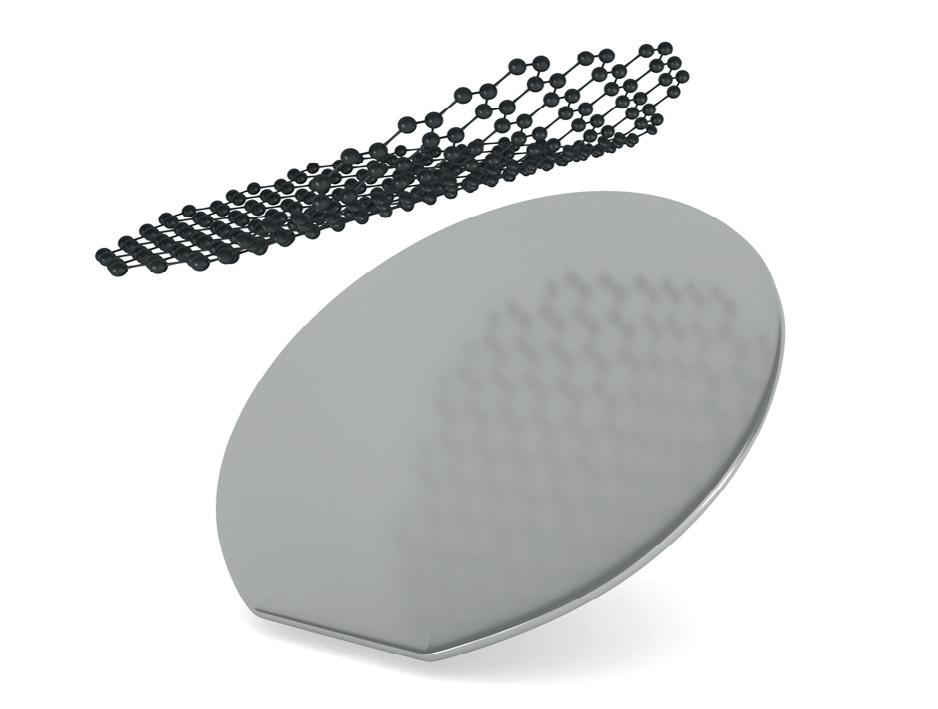
Graphene Flagship researchers report a new method to integrate graphene and 2D materials into semiconductor manufacturing lines. Image credit: A Quellmalz, KTH.
INDUSTRIAL-GRADE ATX MOTHERBOARD
iEi’s IMBA-C2460 ATX motherboard supports 14 nm LGA1151 Intel 8th/9th Generation Xeon E, Core i9/i7/i5/i3, Celeron and Pentium processors with the Intel C246 Chipset. Furthermore, the product features dual-channel ECC supported memory of up to 64 GB for optimal functionality.
The motherboard accommodates triple independent displays (VGA, HDMI and DP++), dual GbE LAN, HD Audio and 6x SATA 6 Gbps ports with RAID 0/1/5/10 for optimal operation. In terms of external I/O interfaces, the product supports 2x USB 2.0 and 2x USB 3.2 Gen 2, 2x USB 3.2 Gen 1, 1x RS-232 and 1x PS/2 port for a legacy keyboard or mouse.
The device is constructed in an effective manner to withstand tough conditions. It has an operating temperature of -20 to +60°C, supported by 1x CPU fan connector and 2x system fan connectors. It holds safety and EMC certifications, as it is CE/FCC compliant. The multifaceted motherboard is therefore suitable when carrying out industrial, medical, transportation, military or other commercial activities requiring long-term product availability. ICP Electronics Australia Pty Ltd www.icp-australia.com.au

Accredited testing and global product approvals since 1992
Bayswater


FLOW METERS/CONTROLLERS WITH ETHERNET POWERLINK
Bronkhorst is a versatile supplier of digital flow and pressure meters and controllers, available in both IP40 and IP65 versions. The company has now added POWERLINK as its 10th onboard fieldbus interface option.
Ethernet POWERLINK (EPL) is a patent-free, manufacturer-independent and completely software-based communication system that delivers real-time performance. Since the fieldbus is based on Ethernet communication, it can be applied with standard Ethernet cabling and support an unlimited number of nodes.
With Bronkhorst’s ‘multi-bus’ concept, the company offers users an extensive choice of 10 fieldbus interface options. The wide range of digital metering and control devices is suitable for many different applications, including the food, beverage and chemical industries; gas and fluid analysis equipment; glass and tool coating processes; testing fuel cells for the automotive industry; and in machinery used to produce electronic chips, LED lights and solar cells. AMS Instrumentation & Calibration Pty Ltd www.ams-ic.com.au
AQUEOUS ASSEMBLY CLEANER
KYZEN’s AQUANOX A4727 aqueous assembly cleaner helps users meet their performance cleaning requirements, with technology that provides a stable pH and predictable compatibility throughout its long bath life.
The product has undergone thousands of hours of laboratory tests and live beta site testing, scientifically validating its good rinsability, long bath life and long-term performance advantages. Its stable chemistry is compatible with a wide variety of components, coatings, labels and equipment.
Engineered to be effective, stable and predictable, the product has been designed to enable ongoing production and assembly operations. Kyzen www.kyzen.com

EXTRUDED ALUMINIUM ENCLOSURES
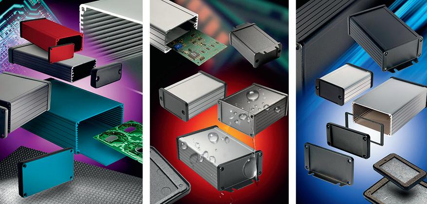
Hammond has introduced additional standard sizes to the 1455U family, available in three standard sizes of 160, 220 and 280 x 191 x 66 mm, in clear and black anodised finish and with aluminium and plastic removable end panels. The family now consists of 32 separate sizes, ranging from 60 x 45 x 25 to 280 x 191 x 66 mm.
There are 15 slot positions for mounting single or multiple PCBs directly into the body. Black, red, yellow, translucent red and translucent blue plastic end panels complete with bezel can be mixed and matched for colour coding. Optional flanged aluminium end panels that enable the unit to be mounted directly to a shelf or wall are also available as an optional accessory to replace the flat panels.
The 1457 IP65 sealed and 1457-EMI screened versions complete the range of options in the new sizes. The 1457U and 1457U-EMI are available in three standard lengths, with clear anodised or black powder-coated bodies and clear or black die-cast aluminium end panels. The 1457 IP65 features a self-adhesive gasket and O rings for the securing screws; the 1457-EMI has a nickel/copper conductive closed foam gasket to preserve continuity between the body and the end panel to give enhanced screening for use in electrically noisy environments.
The enclosures are primarily designed to house PCBs, mounted horizontally into internal slots in the body of the case; they can also be used to house any small electronic, electrical or pneumatic components. All sizes of the 1455 are supplied complete with fixings and self-adhesive rubber feet. Hammond Electronics Pty Ltd www.hammondmfg.com
Expertise you need. Service you deserve.
Test Equipment | Programmable Power | Chambers
• Emissions and immunity testing in a single shielded environment • Meets basic standard: IEC/EN 61000-4-20 • Meets standards for emissions testing: CISPR 14-1, IEC 61000-6-3 and IEC 61000-6-4 for EUT’s without connected cables • Meets standards for immunity testing: EN 60118-13 • Ideal for design qualification and pre-certification
1300 FUSECO (1300 387 326) sales@fuseco.com.au

18 TB HARD DISK DRIVES
Toshiba Electronic Devices & Storage has announced its 18 TB MG09 Series HDDs. The series features the company’s thirdgeneration, 9-disk helium-sealed design and innovative Flux Control – Microwave Assisted Magnetic Recording (FC-MAMR) technology to advance conventional magnetic recording (CMR) density to 2 TB per disk, achieving a total capacity of 18 TB.
With 12.5% more capacity than prior 16 TB models, the drives are compatible with a wide range of applications and operating systems. They are adapted to mixed random and sequential read and write workloads in both cloud-scale and traditional data centre use cases. The HDD features 7200 rpm performance, a 550 TB per year workload rating and a choice of SATA and SAS interfaces — all in a power-efficient, helium-sealed, industrystandard, 3.5″ form factor.
With its power efficiency and 18 TB capacity, the series is designed to help cloud-scale infrastructure advance storage density to reduce capex and improve TCO. As data growth continues at an explosive pace, 18 TB drives with FC-MAMR technology should help cloud-scale service providers and storage solution designers achieve higher storage densities for cloud, hybrid-cloud and on-premises rack-scale storage. Toshiba (Australia) Pty Ltd www.toshiba.com.au

PORTABLE PXI EXPRESS CHASSIS
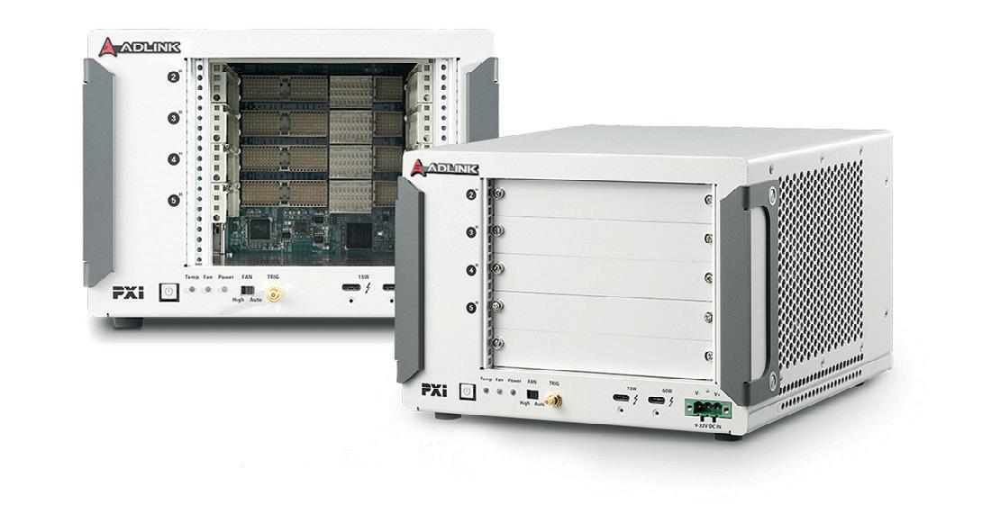
ADLINK Technology has introduced the PXES-2314T PXI Express chassis with versatile, high-bandwidth Thunderbolt 3 interfaces. Unlike traditional PXI Express systems, which are usually large and require complex set-up, the product is a compact test and measurement platform that offers the performance and flexibility of PXI Express but in a portable system, requiring only the small PXES-2314T chassis, a notebook PC with Thunderbolt 3 ports and desired peripheral modules.
The product features two Thunderbolt 3 ports for host PC connections, which use USB Type-C connectors and support USB power delivery up to 60 W and system bandwidth of 40 Gbps. The chassis offers four PXI Express Hybrid slots: two PXIe Hybrid slots up to PCIe Gen2 x1 and two PXIe Hybrid slots up to PCIe Gen3 x4. It measures 207.9 x 148.4 x 220.5 mm, providing a compact system that delivers high performance but saves space, whether on a benchtop or the factory floor.
Targeted use cases for the 4-slot system include performing mobile quality control testing in the production line without sacrificing feature functions or high performance. R&D tests and experiments can be performed flexibly, without requiring investments in older, more cumbersome PXIe systems. The portable device also supports use cases that focus on field troubleshooting, hands-on demos and training for an array of applications in a range of environments. ADLINK Technology Inc www.adlinktech.com
We Stock 1000’s of Plastic Parts for Industry
• Nylon Fasteners • Screws & Nuts • Washers & Spacers • Rivets & Clips • PCB Hardware • Caps & Plugs • Knobs & Handles • Hole Pugs & Bushes • LED Mounts & Light Pipes • Cable Ties & Mounts

avA bali el orf m Q-iH scinortcelE L mi eti d


