A SUPPLEMENT TO DESIGN WORLD MAY 2024 5G,wireless, How do SFP, SFP+, and QSFP compare? Page 19 Wi-fi performance testing now has standards Page 27 Build a 5G open RAN test lab with open-source software tools Page 32 communications handbook & wireline


EDITORIAL
VP, Editorial Director Paul J. Heney pheney@wtwhmedia.com
Editor In-Chief Aimee Kalnoskas akalnoskas@wtwhmedia.com
Senior Technical Editor Martin Rowe mrowe@wtwhmedia.com
Associate Editor Emma Lutjen elutjen@wtwhmedia.com
Managing Editor, EV Engineeering Michelle Froese mfroese@wtwhmedia.com
Design World
CREATIVE SERVICES & PRINT PRODUCTION
VP, Creative Services Matthew Claney mclaney@wtwhmedia.com
Art Director Allison Washko awashko@wtwhmedia.com
Senior Graphic Designer Mariel Evans mevans@wtwhmedia.com
Graphic Designer Shannon Pipik spipik@wtwhmedia.com
Director, Audience Development Bruce Sprague bsprague@wtwhmedia.com
MARKETING
VP, Digital Marketing Virginia Goulding vgoulding@wtwhmedia.com @wtwh_virginia
Digital Marketing Coordinator Francesca Barrett fbarrett@wtwhmedia.com @Francesca_WTWH
Digital Design Manager Samantha King sking@wtwhmedia.com
Marketing Graphic Designer Hannah Bragg hbragg@wtwhmedia.com
Marketing Graphic Designer Nicole Johnson njohnson@wtwhmedia.com
Webinar Manager Matt Boblett mboblett@wtwhmedia.com
Webinar Coordinator Halle Sibly hkirsh@wtwhmedia.com
ONLINE DEVELOPMENT & PRODUCTION
Web Development Manager B. David Miyares dmiyares@wtwhmedia.com
Senior Digital Media Manager Patrick Curran pcurran@wtwhmedia.com
VIDEOGRAPHY SERVICES
Videographer Cole Kistler cole@wtwhmedia.com
Videographer Kara Singleton ksingleton@wtwhmedia.com
PRODUCTION SERVICES
Customer Service Manager Stephanie Hulett shulett@wtwhmedia.com
Customer Service Representative Tracy Powers tpowers@wtwhmedia.com
Customer Service Representative JoAnn Martin jmartin@wtwhmedia.com
Customer Service Representative Renee Massey-Linston renee@wtwhmedia.com
Customer Service Representative Trinidy Longgood tlonggood@wtwhmedia.com
FINANCE
Controller Brian Korsberg bkorsberg@wtwhmedia.com
Accounts Receivable Specialist Jamila Milton jmilton@wtwhmedia.com

WTWH Media, LLC
1111 Superior Ave., Suite 2600
Cleveland, OH 44114
Ph: 888.543.2447
FAX: 888.543.2447


DESIGN WORLD does not pass judgment on subjects of controversy nor enter into dispute with or between any individuals or organizations. DESIGN WORLD is also an independent forum for the expression of opinions relevant to industry issues. Letters to the editor and by-lined articles express the views of the author and not necessarily of the publisher or the publication. Every effort is made to provide accurate information; however, publisher assumes no responsibility for accuracy of submitted advertising and editorial information. Non-commissioned articles and news releases cannot be acknowledged. Unsolicited materials cannot be returned nor will this organization assume responsibility for their care.
DESIGN WORLD does not endorse any products, programs or services of advertisers or editorial contributors. Copyright© 2024 by WTWH Media, LLC. No part of this publication may be reproduced in any form or by any means, electronic or mechanical, or by recording, or by any information storage or retrieval system, without written permission from the publisher.
SUBSCRIPTION RATES: Free and controlled circulation to qualified subscribers. Non-qualified persons may subscribe at the following rates: U.S. and possessions: 1 year: $125; 2 years: $200; 3 years: $275; Canadian and foreign, 1 year: $195; only US funds are accepted. Single copies $15 each. Subscriptions are prepaid, and check or money orders only.
SUBSCRIBER SERVICES: To order a subscription or change your address, please email: designworld@omeda.com, or visit
2 DESIGN WORLD — EE NETWORK 05 • 2024 eeworldonline.com | designworldonline.com
2011 - 2020 2014 Winner 2014 - 2016
2013- 2017


5G, Wireless, & Wired Communications Handbook May 2024
05 Editorial Note
Communications: Its AI or die
06 Flexible PTP profiles ease the transition to 5G
5G brought architecture changes that require synchronization. Depending on the location and network site, those timing requirements require different PTP profiles and PTP capacity.
09 Optimize RF signal quality in 5G power amps
For 5G system performance, obtaining and maintaining the right balance of requirements for high power, power-added efficiency, and signal fidelity is critical. CCDF and PAPR measurements provide insights to help power amplifier designers achieve that goal.
13 How mmWave signals affect cables, connectors, and PCB traces
Millimeter-wave signals used in 5G networks provide wide bandwidth and high data rates. Signal losses, both over the air and through interconnects, bring design challenges.
15 How GaN PAs in 5G radios push test requirements
Proper PA development, validation, and characterization are important because a PA often accounts for a significant portion of a transmitting device's power consumption.
19 How do SFP, SFP+, and QSFP compare?
Pluggable modules come in many variants, each designed for a specific purpose.
24 How to reduce residual noise in 5G NR EVM measurements
Error vector magnitude (EVM) is the most important figure of merit for signal quality in 5G NR. A new method improves measurement accuracy by reducing noise.
27 Wi-Fi performance testing now has standards
Until recently, service providers were unable to predict in-home performance of Wi-Fi devices because they lacked standardized test cases. Now, industry groups have advanced three new standards, each geared toward different Wi-Fi use cases.
29 mmWaves bring challenges to 5G and 6G
Signals in the mmWave range require extra care and more expensive components than at sub-6 GHz frequencies.
32 Build a 5G Open RAN test lab with open-source software tools
Open-source software provides network components that you can use to simulate 5G network functions from the network core to the radio.
34 How do 5G eMBB and FWA data services compare?
Fixed-wireless access is a special use case of enhanced mobile broadband, one of the three use cases specified for 5G. FWA brings different challenges for deployment than eMBB.
Contents
28 16 14 3 DESIGN WORLD — EE NETWORK 05 • 2024 eeworldonline.com | designworldonline.com
Introducing the world’s smallest high-frequency wirewound chip inductor!
Actual Size (Tiny, isn’t it?)
Once again, Coilcraft leads the way with another major size reduction in High-Q wirewound chip inductors
Measuring just 0.47 x 0.28 mm, with an ultra-low height of 0.35 mm, our new 016008C Series Ceramic Chip Inductors offer up to 40% higher Q than all thin film types: up to 62 at 2.4 GHz.
High Q helps minimize insertion loss in RF antenna impedance matching circuits, making the 016008C ideal for high-frequency applications such as cell phones, wearable
devices, and LTE or 5G IoT networks.
The 016008C Series is available in 36 carefully selected inductance values ranging from 0.45 nH to 24 nH, with lower DCR than all thin film counterparts.
Find out why this small part is such a big deal. Download the datasheet and order your free evaluation samples today at www.coilcraft.com.
WWW.COILCRAFT.COM
®
ONMarch 21, 2024, nVIDIA CEO Jensen Huang told us how AI is changing the world. It has surely changed the attitudes of everyone in the data-communications industry.
At OFC 2024, one thing was clear: if you're in the data communications business, you'd better claim that your company helps move AI-related data or risk being left behind. All the data that those GPUs and CPUs need for AI/ML must move in quantities we never dreamed of just two years ago. Yes, AI was already in use before, but now everyone in datacom claims to support it.
Having not attended OFC for several years, I expected to hear the usual claims about the need for faster data rates. Numerous people told me that there was a marked change from 2023, and it was because of AI.
In the recent past, we mostly heard that networks needed more speed for transporting video. We also heard about how 5G would enable those faster mobile downloads. Many people I spoke to at OFC claim that data demands from AI will soon greatly exceed those from video, overwhelming datacenters with data. Everywhere I turned, there was a booth touting AI and how that company's product — be that network switches, optical network components, semiconductors, and test equipment — would enable it. That put people at OFC 2024 on edge, making them a little jittery. They were wondering if optical data rates could keep up with the coming demand for moving data. They were not concerned about AI taking away their jobs but with how the industry could possibly keep up. Moreover, they were feeling the need to beat their competitors to the next speed.
Optical link rates of 400 Gb/sec (4 x 100 Gb/sec) and 800 Gb/ sec (8 x 100 Gb/sec) are in use today, and they were everywhere at OFC. Some companies claimed they are already moving toward 1.6 Tb/sec, known as 1.6T. A few mentioned 3.2T and one presentation included a timeline to 6.4T.
The demand for faster data transport may finally result in the deployment of technologies that have been on the table for some time. Silicon photonics is one such technology. We've been hearing about it for years, but now, moving data electrically on boards and in semiconductors may no longer meet demand. Coherent optics is another technology that has gained importance, both in OFC exhibithall products and technical sessions.


common in wireless communications. Coherent optics modulates amplitude, frequency, and polarization, which increases data rates on a fiber.
Today, DSP chips in the optical modules convert signals from electrical to optical and back. The DSP takes electrical digital signals, retimes them, and converts them into analog to drive the optical engine.
Linear-drive optics (LDO), also called linear-drive pluggable optics (LPO), moves the DSP out of the pluggable optical module and into the network switch. With LDO, the electrical signal arrives in the module in analog form, ready to drive the laser. Shifting to LDO can reduce energy consumption, size, and cost in optical modules. AI is expected to bring many more optical cables to data centers and move computing from the cloud to the network edge. Moving DSP chips to the switch makes them easier to cool, and there's no need to replace the DSP just because the module needs replacement.
The need for speed is already pushing 224 Gb/sec electrical links. Once it's in production, we'll see 800G optical links running on 4 x 200 Gb/sec lanes. The moment that happens, the race for 1.6T (8 x 200 Gb/sec lanes) commences. In my experience, what we hear at OFC regarding data rates translates into talks at the following year's DesignCon.
Cheers,
It uses I/Q modulation, which is
 Martin Rowe, Senior Technical Editor
EDITORIAL NOTE
5 DESIGN WORLD — EE NETWORK 05 • 2024 eeworldonline.com | designworldonline.com
Flexible PTP profiles ease the transition to 5G
5G brought architecture changes that require synchronization. Depending on the location and network site, those timing requirements require different PTP profiles and PTP capacity. Eric Colard, Microchip Technology
AScritical infrastructure such as telecommunications, utilities, transportation, and defense migrate from 4G to 5G, you might assume that these essential services universally adopt the ITU-T G.8275.1 Precision Time Protocol (PTP) profile for time synchronizing their networks [1]. After all, PTP embeds a superior quality PTP boundary clock (BC) compared to 4G. This tendency, however, could understate that 5G mobile synchronization has become more granular.
Time division duplex (TDD) in 5G brings new phase requirements, both relative and absolute. It also introduces Open RAN [2], with baseband unit (BBU) functions disaggregated into Radio Units (RUs), Distributed Units (DUs), and Centralized Units (CUs). As a result, the telecom industry has standardized two PTP profiles, ITU-T G.8275.1 and ITU-T G.8275.2, to address PTP-aware and PTP-unaware networks, respectively [3].
Synchronization issues
Operators understand the implications of having a backhaul network. Depending on the type of network, packet-delay variation (PDV) can have a major impact on synchronization. In many countries, PTP was deployed in 4G as a backup synchronization mechanism, while Global Navigation Satellite System (GNSS) was the primary synchronization source. To avoid a situation where a GNSS failure leads to the loss of phase services, the idea of connecting the edge primary reference time clock (PRTC) to the centralized core clock using a PTP flow was developed [4]. It was adopted by the ITU-T as G.8273.4 [5] — Assisted Partial Timing Support (APTS).
In this architecture, the PTP input is calibrated for time error using the local-edge PRTC GNSS. This GNSS has the same reference (Universal Coordinated Time, UTC) as the upstream GNSS. You can consider the incoming PTP flow a proxy GNSS signal from the core with traceability to UTC.

Figure 1. A typical synchronization architecture for mobile 4G uses a grandmaster clock and the G.8275.2 PTP profile.
Figure 1 shows a typical 4G synchronization scenario where a PTP grandmaster serves 4G eNodeBs over a backhaul using PTP unicast G.8275.2 profile.
6 DESIGN WORLD — EE NETWORK 05 • 2024 eeworldonline.com | designworldonline.com 5G, WIRELESS, & WIRED COMMUNICATIONS HANDBOOK
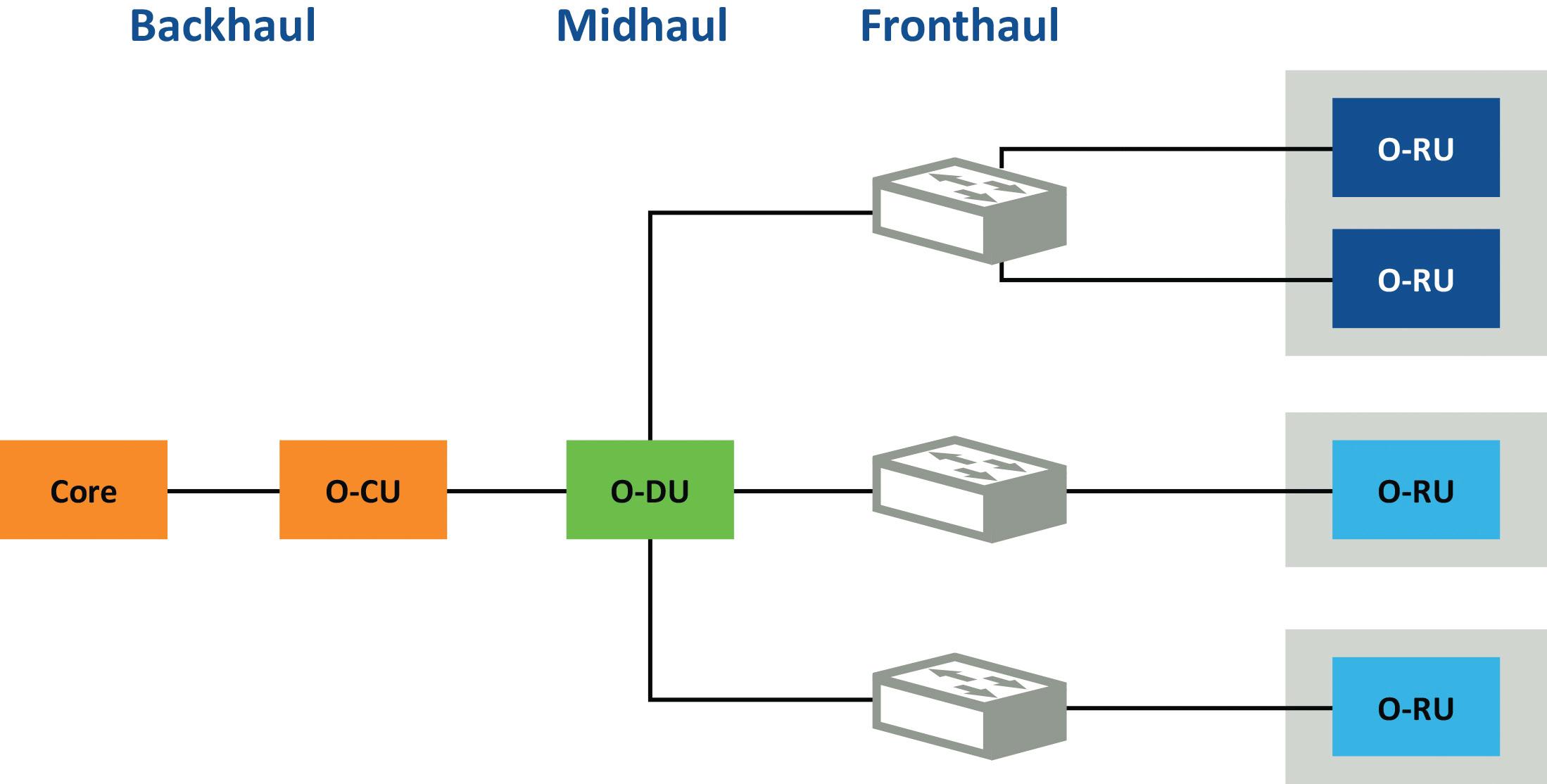
2. An Open RAN 5G network architecture, disaggregates the BBU, which adds devices to the network and makes synchronization more complex.
5G needs a new synchronization architecture because the mobile network has become increasingly complex due to the Open RAN disaggregation. Figure 2 shows the key elements of a 5G architecture.
Operators need to consider the backhaul in addition to a typical 5G architecture. Furthermore, disaggregation introduces fronthaul and mid-haul networks.
From a synchronization standpoint, the fronthaul becomes the focal network point for serving 5G RUs or 5G base stations. Figure 3 shows how a fronthaul network serves 5G base stations (gNodeBs) using G.8275.1 multicast profile. In this scenario, PTP becomes the primary synchronization mechanism.
Important considerations when implementing 5G include the end-toend timing budget (±1.5 µsec) and the 130 nsec/260 nsec relative-time accuracy between adjacent RUs, as shown in Figure 3.
ITU-T G.8275.2 profile, on the other hand, resides at layer 3, unicast. It doesn't require on-path support capability on all the network elements. The PTP protocol flows through those network elements as highpriority traffic. In this use case, the network needs large PTP client capacity support from the PTP grandmaster, typically over one hundred clients and up to several thousand in some cases.
Fronthaul profile
Fronthaul, from a synchronization standpoint, operates from a source of time from a GNSS signal. Assisted Partial Timing Support (APTS) protects it in situations when the GNSS signal is unavailable or intermittent.
Fronthaul typically resides in large cities and metro areas that contain many base stations. PTP grandmasters located nearby serve the base station. In this situation, the network uses a profile based on G.8275.1, a PTP profile defined specifically for the telecom industry with network elements that embed a modern boundary clock. G.8275.1 uses multicasting mode, which doesn't require a lot of capacity.
To date, PTP provides frequency synchronization outside of metro areas.
Grandmaster clocks deployed at these locations serve mainly older FDD radio systems. Increasingly, these clocks are part of a mix of older radios and new environments brought to the deployment by the move to 5G.
Many operators are migrating frequency-focused grandmasters to newer generations of IEEE 1588 PTP grandmasters that support 5G requirements through better time and phase accuracy. These clocks also provide additional capabilities and more PTP ports than prior generations. The new grandmasters must connect to many more devices, including older radios, cell towers, and other PTP grandmasters.
These backhaul sites and grandmasters typically utilize the ITU-T G.8275.2 profile,

7 DESIGN WORLD — EE NETWORK 05 • 2024 eeworldonline.com | designworldonline.com NETWORK TIMING
Figure
Figure 3. A 5G typical synchronization architecture where the fronthaul serves gNodeBs while the backhaul also serves eNodeBs for 4G.
which runs at the internet protocol (IP) layer. The telecom industry focuses on enabling migrations of legacy environments towards newer architectures and devices. Existing legacy signal systems such as Synchronization Supply Units (SSU) and Primary Reference Clocks (PRC) are not going away and need integration into the newer architectures focused on 5G and PTP. Another aspect to consider beyond capacity is the ability to integrate systems located at sites distant from the grandmasters:
Moving into 5G
Operators adding 5G mobile services can leverage existing synchronization investments and build upon them. Typically, large operators will install PTP grandmasters in central offices that support wireline broadband and wireless mobility. This leads to four typical use cases.
• Operators use a dedicated Primary Reference Source (PRS), which is common in North America. In those instances, operators will often replace the legacy PRS systems and migrate to a newer generation grandmaster that can function as a PRS or enhanced PRS (ePRS).
• Operators migrate from a traditional PRTC grandmaster to a more modern platform. This provides more connectivity options and advanced APTS capabilities as well as frequency synchronization for cell site backhaul (thousands of clients) using PTP G.8275.2.
• Operators will deploy new PRTC grandmasters for 5G fronthaul using PTP G.8275.1
• Operators migrate existing synchronization systems to more modern and resilient PTP grandmasters that meet stringent 30 ns accuracy to UTC, as well as 14 days holdover in selected sites.
These installations preserve investments. Over time, operators leverage newer technologies to serve 5G sites through an evolution of existing synchronization infrastructure.
Other market dynamics
Aside from the fronthaul and backhaul considerations for choosing a timing profile and capacity requirements, some countries or operators may not own the infrastructure for part or all their deployments.
In North America, operators commonly lease backhaul lines from third parties. These leased lines, however, don't always meet the operator's time and phase performance requirements. Mobile operators can't always rely on the backhaul links and may lack the means to monitor the synchronization quality that third-party leased-line providers deliver.
To serve mobile operators and ensure high accuracy given the stringent timing requirements for 5G architectures, leased line backhaul providers are upgrading their network elements with boundary clocks to deliver highly accurate time and phase to operators.
New entrants such as satellite providers or cable operators are adding mobile to their portfolio. They also rely on third parties to
deliver precise time over the leased architecture. Legacy wireline providers often lease their wireline infrastructure to mobile operators and new mobile entrants. Leased-line providers may need to upgrade their infrastructure to serve mobile operators with accurate time and phase. Mobile operators can then run either G.8275.1 or G.8275.2 over the leased backhaul layer. Operators leasing lines should make sure third-party providers can guarantee a level of time accuracy.
No one-size-fits-all
A mobile operator deploying a 5G architecture or launching a 5G service has options based on standards that can be deployed at the fronthaul network and the backhaul network. This will lead to various PTP profiles as well as various PTP capacity levels depending on the region, network transport, and integration requirements.
References
1. G.8275.1: Precision time protocol telecom profile for phase/ time synchronization with full timing support from the network. International Telecommunications Union. https://www.itu.int/rec/TREC-G.8275.1-202211-I/en
2. Gile, Darrin, "Open RAN Networks pass the time," 5G Technology World, April 4, 2023. https://www.5gtechnologyworld. com/open-ran-networks-pass-the-time/
3. G.8275.2: Precision time protocol telecom profile for phase/ time synchronization with partial timing support from the network. International Telecommunications Union. https://www.itu.int/rec/TREC-G.8275.2/en
4. Olsen, Jim, "How Virtual Primary Reference Time Clocks improve 5G network timing," 5G Technology World, March 3, 2021. https:// www.5gtechnologyworld.com/how-virtual-primary-reference-timeclocks-improve-5g-network-timing/
5. G.8273.4: Timing characteristics of telecom boundary clocks and telecom time slave clocks for use with partial timing support from the network, International Telecommunications Union, https://www. itu.int/rec/T-REC-G.8273.4/en
8 DESIGN WORLD — EE NETWORK 05 • 2024 eeworldonline.com | designworldonline.com 5G, WIRELESS, & WIRED COMMUNICATIONS HANDBOOK
Optimize RF signal quality in 5G power amps
For 5G system performance, obtaining and maintaining the right balance of requirements for high power, power-added efficiency, and signal fidelity is critical. CCDF and PAPR measurements provide insights to help power amplifier designers achieve that goal.
Bob
Buxton, Boonton/Wireless Telecom Group, Maury Microwave
WHILE
all parts of the 5G RF signal chain contribute to overall system performance, the transmitter power amplifier (PA) has characteristics that require careful attention. Nonlinear PA performance can be a critical factor that negatively impacts error-vector magnitude (EVM) and bit-error rate (BER).
Insufficient input back-off (IBO) causes compression leading to EVM degradation, which reduces the peak-to-average power ratio (PAPR) of OFDM/m-QAM signals. Increasing IBO will restore PAPR to the required level but with a penalty for amplifier efficiency and the costly need to use a higher power PA. For these reasons, you need to find the optimum IBO setting point.
5G signal chain
The 5G transmitter signal chain starts with a digital baseband and beamforming processing and extends to the antenna array. Figure 1 shows the PA as the active component at the end of the line. PAs often use Doherty amplifiers to maximize efficiency [1].
PAs often use GaN technology, although other technologies, such as CMOS-SOI, are under consideration for the FR3 band [2]. The telecom industry has its sights set on FR3, which runs roughly from 7 GHz to 24 GHz. Whatever technology is used, obtaining a balance


Figure 2. Orthogonality in OFDM signals occurs through proper subcarrier spacing.
between high output power, power-added efficiency (PAE), and signal fidelity is always a major consideration. To see how these factors interrelate, we’ll start with a look at the nature of 5G signals.
5G RF signals
5G uses orthogonal frequency division multiplexing (OFDM), where the multiple subcarriers are modulated by quadrature amplitude modulation (m-QAM) of up to 1024-QAM. Orthogonality occurs through spacing the subcarriers by the inverse of the symbol time (T). As shown in Figure 2, this ensures that subcarrier peaks align with the nulls of the other subcarriers, which prevents inter-subcarrier interference.
5G’s numerology defines a range of subcarrier spacings. In the sub-6 GHz FR1 band, these are 15 kHz, 30 kHz, and 60 kHz [3]. 30 kHz corresponds with an OFDM symbol time of 33.3 µs.
Because the subcarriers are transmitted simultaneously with a continually varying phase relationship determined by their frequency
Figure 1. This simplified block diagram of a 5G massive MIMO transmitter chain highlights power amplifiers.
9 DESIGN WORLD — EE NETWORK 05 • 2024 eeworldonline.com | designworldonline.com POWER AMPLIFIERS

3. A summation of the signals shown in the time domain shows a high PAPR (solid trace).
spacing, the subcarriers can sum, causing high power level peaks, as shown in Figure 3. The level of these peaks relative to the average level of the signal is characterized as the signal’s PAPR.
When driving a PA with a high PAPR signal, the peaks of the signal drive into the amplifier’s non-linear region, which can result in spectral regrowth, causing adjacentchannel leakage. IBO can reduce the peak levels, constraining them to the linear region. Unfortunately, doing so also reduces the average power. The amplifier no longer operates at its ideal point for maximum efficiency, as shown in Figure 4.
To regain some efficiency, you can apply various techniques that intentionally reduce PAPR and thus reduce IBO [4]. You must limit the degree of PAPR reduction to that consistent with meeting EVM targets.

4. An amplifier's point of maximum efficiency occurs just before it reaches the saturation region.
Once the PA reaches that level, be sure that PA non-linearity doesn't further reduce PAPR. Otherwise, that could increase EVM and lead to symbol errors, as shown in Figure 5.
Measuring EVM requires equipment such as signal analyzers. Because we are concerned with the impact of an amplifier’s nonlinearity on reducing the signal’s PAPR, you can use a cost-effective, direct measure of that effect.
Linearity characterization
You can apply any of several methods to characterize amplifier linearity. Two common methods are to measure the 1 dB compression point (P1db) and to measure the third-order intercept point (TOI). Both methods use CW signals and average power measurements. Because these methods use
signals that don't represent the OFDM/mQAM signals, they won't provide sufficient information about the response to signals with high PAPR levels.
Noise power ratio (NPR) is another measurement method for assessing amplifier linearity. It is effective as an indicator of spectral regrowth caused by nonlinearity. Because NPR uses additive white-Gaussian noise (AWGN), it's also more representative of real-world performance. It does, however, require expensive test equipment. Strickler, Correa, and Bollendorf compare this and other methods for assessing amplifier nonlinearity [5].

Figure 5. Clipping the peaks reduces the vector length, potentially causing symbol errors.

Figure 6. A plot of EVM vs. PAPR shows their relationship [6].
10 DESIGN WORLD — EE NETWORK 05 • 2024 eeworldonline.com | designworldonline.com 5G, WIRELESS, & WIRED COMMUNICATIONS HANDBOOK
Figure
Figure
A “real-world” view
Getting back to the end objective, how can we assess the effect of an amplifier’s linearity, or rather non-linearity, on EVM performance? Figure 6 shows experimental results for the relationship between EVM and PAPR.
In this case, the slope of the curve is approximately 3% degradation in EVM per 1 dB reduction in PAPR. The slope may differ for different modulation schemes. Establishing the slope through making PAPR and EVM measurements early in development means, however, that you can use PAPR as a simple, quick, and costeffective predictor of amplifier performance on EVM. This avoids making repeated EVM measurements when changing IBO or amplifier design. It also means that you can use PAPR rather than EVM in production tests, which leads to a paradigm shift in amplifier manufacturing.
Measuring PAPR and CCDF
How can you execute a practical method for measuring PAPR? You can use a highsample-rate signal analyzer to make PAPR measurements. Recall that for making EVM measurements, such equipment is expensive, complicated, and occupies significant bench space.
Instead, you can use a power sensor. Available from several manufacturers, power sensors commonly use a diode as the sensing element. Diode-based average power sensors can measure a signal’s average power independent of modulation
type. Because these sensors have a relatively slow response time, they don't provide the instantaneous peak-envelope measurements required to obtain PAPR results.
Peak-power sensors are fast enough to track a signal’s power envelope and provide high-sample-rate instantaneous peak power results. They have sample rates of some 100 MSamples/sec, and when measuring repetitive signals, random interleaved sampling can yield effective sample rates of 10 GSamples/sec. That enables 100 ps time resolution.
To faithfully track the power envelope fluctuations of a wideband modulated signal, the sensor needs to have a wide video bandwidth and an associated fast rise time. In the case of a 100 MHz wide 5G FR1 channel, a sensor with less than 100 MHz video bandwidth (VBW) would not provide accurate results, whereas a sensor with, say, 165 MHz VBW would. Such sensors are available from several manufacturers.
Using peak-power sensors configured as shown in Figure 7, you can the measure RF signal's peak, average, and minimum power at the amplifier's input and output.
Figures 8a and 8b show instantaneous envelope power vs. time for signals with light and heavy signal compression. Figure 8a shows the input signal (CH1) and the output signal (CH2) from an amplifier operated mainly in its linear region. The output crest factor, another way of saying its maximum PAPR, reduces by just 0.6 dB compared to the input signal. In Figure 8b, with a reduced


Figure 8. Light compression of peaks (a) shows a 0.6 dB difference in PAPR, while (b) heavier peak compression increases PAPR to 3 dB.
IBO, that difference increases to 3 dB, which indicates that the amplifier is operating further into its nonlinear region and imposing a much higher degree of compression.
Measuring the crest factor alone provides no statistical context. The complementary cumulative distribution function (CCDF) provides valuable additional information.
CCDF curves show the percentage of time (Y-axis) that the PAPR (X-axis) is greater than a specific value. Figures 9a and 9b show
Figure 7. Using two peak-power sensors, you can simultaneously characterize a 5G power amplifier.
11 DESIGN WORLD — EE NETWORK 05 • 2024 eeworldonline.com | designworldonline.com POWER AMPLIFIERS

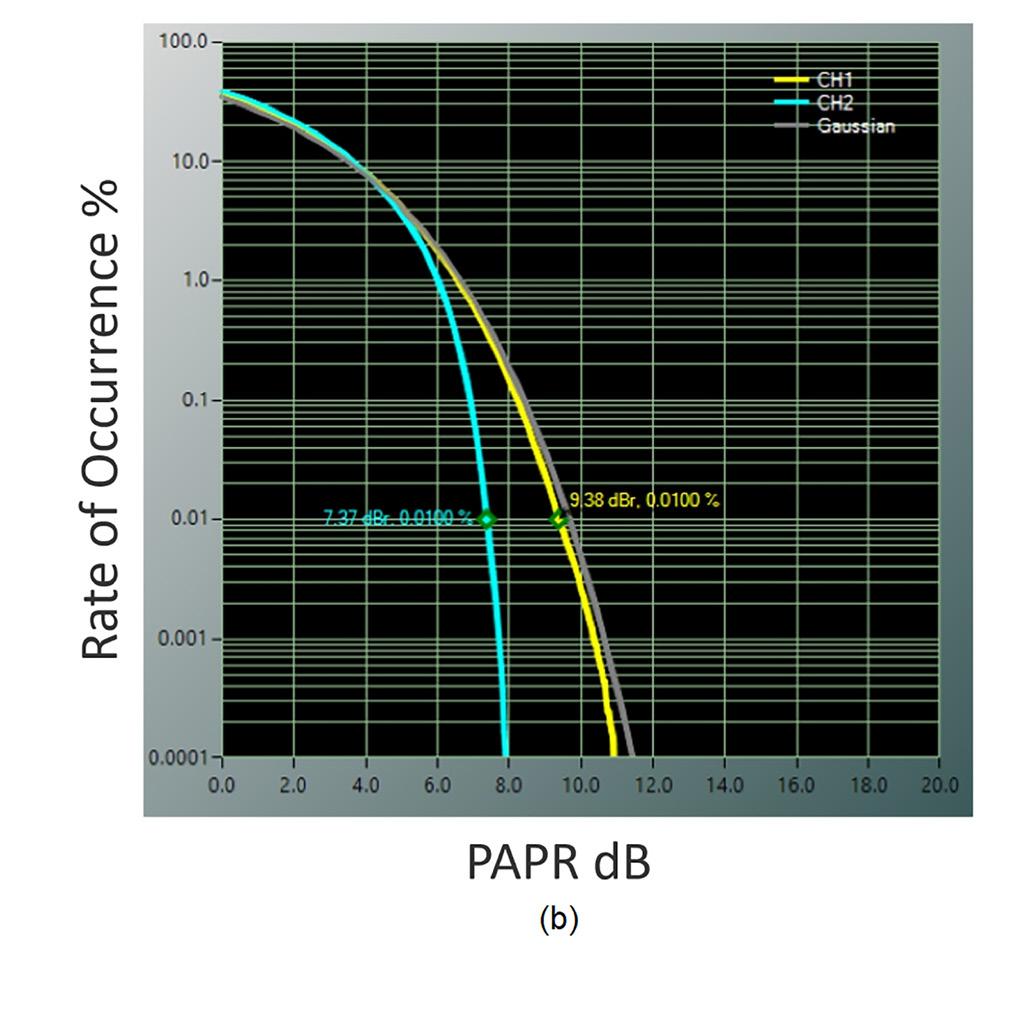
Figure 9. CCDF curves show that hanging the IBO, as done in Figure 8, reduces PAPR 99.99% of the time.
CCDF curves for the same signals shown in Figures 8a and 8b. Plot 9a shows the results when an amplifier is operated in what is essentially its linear region for all but the highest peaks. The input signal (CH1) peaks are >9.4 dB relative to the average signal level for 0.01% of the time. The output of the amplifier (CH2) has peaks >9.2 dB relative to the average signal level for 0.01% of the time.
When the IBO has been reduced, as shown in Figure 9b, the output CCDF (CH2) shows that for 0.01% of the time, the peaks now only exceed 7.4 dB instead of 9.2 dB. Essentially this means the signal’s maximum PAPR had been reduced by 1.8 dB for 99.99% of the time. Using the -3%/dB slope derived from Figure 6, this reduction in PAPR indicates an EVM degradation of approximately 5.4%.
Using a combination of peak power sensors and the CCDF lets you obtain rapid, near real-time results while adjusting IBO or other amplifier parameters. This allows you to find the optimum point on the amplifier’s linearity curve to balance IBO and PAE. In a production test, you need only monitor changes in PAPR to ensure you're meeting EVM targets.
By leveraging a relationship between EVM and PAPR, you can measure PAPR reduction, which indicates EVM degradation, instead of expensive signal analyzers. Once you find the minimum level of PAPR, you can employ peak-power sensors to characterize PAPR and CCDF as a simple, fast, and cost-effective way to verify that you've attained the desired PAPR, and hence EVM.
References
1. Bob Witte, How Doherty Amplifiers improve PA efficiency. 5G Technology World. March 8, 2021. https://www.5gtechnologyworld. com/how-doherty-amplifiers-improve-pa-efficiency/
2. Sravya Alluri, Vinent Leung, Peter Asbeck, A Compact 27 dBm Triple-Stack Power Amplifier for 13 GHz Operation in CMOS-SOI. 2024 IEEE Topical Conference on RF/Microwave Power Amplifiers for Radio and Wireless Applications.
3. ETSI TS 138 101-1 V17.9.0 Table 5.3.2-1
4. Yasir Rahmatallah and Seshadri Mohan, Peak-To-Average Power Ratio Reduction in OFDM Systems: A Survey And Taxonomy. IEEE Communications Surveys & Tutorials, vol. 15, no. 4, fourth quarter 2013.
5. Walt Strickler, Paulo Correa, and George Bollendorf, A Better Approach to Measuring GaN PA Linearity. Microwave Journal, June 14, 2020. https://www.microwavejournal.com/articles/print/34081a-better-approach-to-measuring-gan-pa-linearity
6. Chart Source: Kim, D., An, S. Experimental analysis of PAPR reduction technique using hybrid peak windowing in LTE system. J Wireless Com Network 2015, 75 (2015). https://doi.org/10.1186/ s13638-015-0282-9
12 DESIGN WORLD — EE NETWORK 05 • 2024 eeworldonline.com | designworldonline.com 5G, WIRELESS, & WIRED COMMUNICATIONS HANDBOOK
How mmWave signals affect cables, connectors, and PCB traces
Millimeter-wave signals used in 5G networks provide wide bandwidth and high data rates. Signal losses, both over the air and through interconnects, bring design challenges. Ketan Thakkar, Cinch Connectivity Solutions
MILLIMETER
wave (mmWave) signals offer engineers countless application possibilities, including ranging, object detection, and mapping. Unfortunately, mmWaves bring numerous design challenges. Not only do mmWave signals cover short ranges, but they can suffer from losses as they travel through cables, connectors, and PCB traces. You can, however, minimize losses through solid design practices.
mmWave refers to RF signals with wavelengths typically between 1 mm and 10 mm, covering frequencies from roughly 30 GHz to 300 GHz (Figure 1). In terms of 5G, mmWave starts at 24 GHz. This band of frequencies is often referred to as Extremely High Frequency (EHF), with Super High Frequency (SHF) being below EHF and Tremendously High Frequency (THF) above it.
At mmWave frequencies, signals lose strength from absorption in the atmosphere, which limits their travel distance. This absorption results from the presence
of oxygen in the atmosphere, both in elemental form and in water vapor. While such signal degradation is often a drawback in many radio systems, it is surprisingly useful for high-bandwidth networks.
By preventing signals from traveling too far, you can reuse the same frequencies in other nearby networks without interference. The higher frequency of mmWave compared to Wi-Fi also allows for far more bandwidth, which is one of the many reasons why 5G networks utilize mmWave.
The wide bandwidth of mmWave leaves plenty of room for expansion, meaning that mmWave is unlikely to become congested for the foreseeable future. The high frequency also means that equipment can use small antennas, making them easy to integrate into small devices. This small size also makes the construction of small-scale phased array antennas feasible.
Phased arrays make beamforming possible, which lets multiple devices share the same frequency without interfering with each other. mmWave systems (especially 5G) can handle thousands of

devices simultaneously while ensuring that each device can take full advantage of the bandwidths offered by the higher frequencies.
Unlike signals at lower frequencies, mmWave is extremely directional, operating more like a laser beam than a wave that diverges drastically from its source. This means that mmWave applications operate more on a line-of-sight basis, thereby reducing interference between different mmWave devices.
What challenges does mmWave introduce?
You might think that mmWave's high bandwidth capabilities, lack of interference, and directional nature make it the ideal frequency range for any communication network. That's not necessarily the case. High attenuation from the atmosphere often limits transmission distances to just 100 m, though experiments have reached distances of 10 km under the right conditions. In the case of 5G networks, the high attenuation, and resulting short range requires numerous 5G cells near users, which significantly increases the cost of building and maintaining a reliable network.
Of course, this would apply to any mmWave network, including those used in consumer, commercial, and industrial
Figure 1. RF spectrum highlighting the mmWave region.
13 DESIGN WORLD — EE NETWORK 05 • 2024 eeworldonline.com | designworldonline.com MMWAVE CONNECTIONS
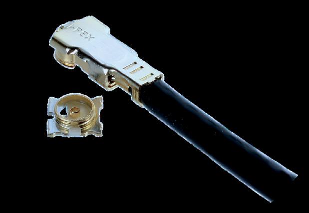
Figure 2. SMA and SMP RF cable assemblies minimize signal losses at mmWave frequencies.
environments. This is why other network technologies utilizing lower frequencies such as 2.4 GHz and 5 GHz Wi-Fi are often preferred.
The high frequencies associated with mmWave can push traditional semiconductors to their limits. For example, circuits utilizing traditional silicon can't go beyond 190 GHz, making the entire frequency range above 190 GHz inaccessible. That's why other processes, such as GaN, come into use.
PCB traces
When operating at mmWave frequencies, PCB traces become more complicated because of signal degradation. Furthermore, PCBs also introduce numerous challenges in their design, including interference from other circuits, the choice of dielectric, subtle variations in identical PCBs, and even environmental conditions of the day. (For example, the direction of cleaning copper clad layers during manufacture can change the signal integrity performance of a trace).
Furthermore, trying to get mmWave frequencies to travel through a PCB can also challenge you because signals can radiate from the tail ends of vias that are not fully connected. The change in material from trace to via can also induce losses and reflections, which are only more problematic in connectors. This is especially true for connectors that utilize mating contacts where the contact point between two connectors isn’t at the ends of the contacts.
If long cable lengths carry mmWave signals, then the exact length of that cable assembly will determine the signal degradation; mismatched lengths and

impendences will result in reflections. At low frequencies, slight mismatches are not massively degrading, but when dealing with mmWave, even the smallest mismatch can destroy signal fidelity.
What can you do?
You can follow numerous steps to solve the numerous challenges that mmWave frequencies bring. Unfortunately, you can’t skip any of these steps.

First, any connector, cable, or PCB trace intended to carry mmWave signals needs construction that uses high-grade materials to minimize signal loss. Furthermore, they should also be rated for the expected frequency ranges.
To minimize signal losses, connectors should make full contact along the entire conductor. All conductors need termination. Connectors often use a cage whereby a socket connector can grab and fully enclose a plug connector from the tip to the base. Figure 2 shows examples of such connectors.
For designs that require PCB traces, you must ensure that traces avoid turns and vias. If you must use vias, then you must terminate the end of the via with a trace. Unconnected vias not only act as reflection points; they can also radiate signals, which introduces EMI issues.
Any mmWave communication between two boards takes place through coax cables or flyover cables, but the length of the cable should carefully match the wavelength of the intended signal.
Cables and connectors
Engineers have numerous options from many companies for connecting mmWave systems, such as quick-connect connectors. These assemblies utilize high-quality dielectrics and conductor materials and are manufactured to specific sizes and lengths to reduce signal reflections. These are commonly used in high-volume manufacturing due to the reduced mating/de-matting time and the availability of ganged connectors.
simplifies the installation of mmWave cabling. For applications that have specific requirements, many manufacturers also offer custom cable assemblies that provide phase matching or can operate in extreme environments.
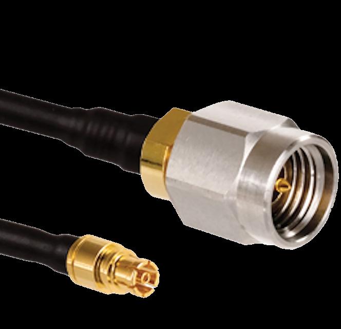
The choice of connector mounting is also essential in any mmWave design. Angled connectors (30° and 45° with respect to PCB) are ideal for use for a wide range of frequencies (up to 26.5 GHz). Angled connectors (Figure 3), available from numerous manufacturers, provide strain relief to cables (essential in mmWave applications) and improve voltage standing wave ratio (VSWR) ratings (up to 1.30) compared to vertical (90°) mount connectors.
Some mmWave systems can experience shock and vibration. For these applications, SMP3 coax connectors can help engineers thanks to their 30% smaller design compared to SMPM and a floating bullet. With a maximum frequency of 67 GHz and a VSWR of 1.50, these connectors offer engineers options for mmWave applications in harsh environments.
Conclusion
mmWave's high frequency, large bandwidth, line-of-sight behavior, and easy manipulation through miniature phased arrays can provide wireless devices with high data rates. For all the benefits that it provides, it also faces numerous challenges if not properly addressed. Thus, you must understand the design constraints that mmWave presents, use best RF practices when designing PCBs, and carefully choose connectors made from high-quality brass, beryllium copper, or stainless steel to ensure ruggedness and high performance.
14 DESIGN WORLD — EE NETWORK 05 • 2024 eeworldonline.com | designworldonline.com 5G, WIRELESS, & WIRED COMMUNICATIONS HANDBOOK
Figure 3. Angled RF connectors reduce cable strain and improve VSWR.
How GaN PAs in 5G radios push test requirements
Proper PA development, validation, and characterization are important because a PA often accounts for a significant portion of a transmitting device's power consumption.
Chen Chang and Alejandro Escobar Calderon, NI
SILICON
has proven a reliable, cost-effective, and easy-to-manufacture material in most chipsets and components. As the world moves more and more to a digital, interconnected, and device-driven ecosystem, however, the need for more performance, throughput, and efficiency increases. While silicon still has endless use cases, it can't meet the performance requirements needed for 5G New Radio (NR), which requires higher power, higher operating temperature, and better efficiency. Wide bandgap semiconductors will help meet this need. When it comes to high-power RF applications, Gallium Nitride (GaN) is set to change the high-power RF power amplifier (PA) game.
Depending on the application, the definition of high-power may change. For now, a high-power PA will have a P1dB compression point of at least 30 dBm, perhaps as high as 70 dBm. Due to the lower bandgap, traditional power-amplifier topologies such as HBTs and pHEMT amplifiers on GaAs substrates are not optimal. Instead, high-power PA designers typically opt for either LDMOS FETs on an SiC substrate or HEMT amplifiers built with a GaN layer on top of a SiC substrate. Figure 1 shows the differences in bandgaps among semiconductor materials.

GaN offers many advantages over traditional semiconductors. Being a wide bandgap device means that it offers better power efficiency at high frequencies, higher operating temperatures, higher power, and better power density than other processes. Because of those differences, you'll need to alter your test strategy.
Although the exceptional power, temperature, efficiency, and frequency properties of GaN have been known for decades, certain technical challenges have limited its viability in commercial applications. For example, the ability for GaN ICs to be produced using traditional silicon semiconductor manufacturing technology has opened the door to GaN
PAs on a larger scale. Furthermore, today’s increased need for higher-power and more efficient components that function across various frequency bands and compatibility with 5G NR and legacy cellular standards (Figure 2) means leads to a significant increase in interest.
Because of their wide bandgap characteristics, GaN PAs are well-suited to address many issues when implementing modern base station infrastructure for cellular communications. GaN PAs could greatly benefit the development of wireless infrastructure. Applications include the need for greater power efficiency, operation across multiple bands and frequencies that accommodate both new and legacy cellular
POWER AMPLIFIERS 15 DESIGN WORLD — EE NETWORK 05 • 2024 eeworldonline.com | designworldonline.com
Figure 1. GaN's wide bandgap makes it the top contender for use in 5G power amplifiers.

standards, and efficient operation across wideband waveforms.
A traditional base station (Figure 3) includes three devices: a baseband unit (BBU) at the base of the tower, a remote radio unit (RRU) at the top of the tower, and an antenna. The RRU will include the hardware for separating the uplink and downlink signals, amplifying the signals, up/ down converting, and signal conditioning. The high-power PA resides on the TX path within the RRU. In the base station, GaN PAs present many benefits, including the ability to accommodate multiple frequency bands to support multiple devices simultaneously.
Despite all the potential benefits, GaN PAs present many challenges in tests due to their unique characteristics. Some of these include:
· Complex test setups
· GaN linearization
· Accurate power measurements
· Time-domain synchronization
· Novel processes and technologies
Complex test setups
A high-power PA is often a combination of multiple smaller PAs. Sometimes multiple stages are cascaded in series into a single
high-gain PA. Another common amplifier architecture is known as a Doherty amplifier, in which two amplifiers connect in parallel, both receiving a split copy of the signal. One amplifier (known as the carrier PA) is tuned to accurately amplify the lower-power portion of the signal while the other amplifier (known as the peaking PA) is tuned for the higher-power portion. The signals are then recombined, giving improved signal fidelity across both operating regions.
Even with these multistage techniques, the amplifier’s output power is often still insufficient for commercial applications. A driver amplifier boosts the signal power ahead of the high-power PA. The driver amplifier is normally optimized for high linearity and low noise figures because its input is closer to the noise floor.
In addition to the physical test setups, the bring-up of GaN PAs can also be more intricate and involved than with other RF power amplifiers. For example, DC biasing must be applied to the DUT before generating or acquiring any RF waveforms.
Linearization
Base stations must analyze uplink signals and generate downlink signals across
compatible with both new and legacy cellular standards.
multiple bands simultaneously. With multiple antennas and signal chains active on a single tower, congestion can occur, both physically as towers become more crowded and spectrally as cellular traffic increases. This drives designers to optimize signal chains in several ways. Some signal chains need optimizing for multiple bands, meaning the PA must operate across these bands simultaneously. This results in strict requirements on out-of-band spectral emissions, as nearby antennas are transmitting and receiving at those nearby frequencies.
In addition, GaN PAs tend to behave with less linearity than more traditional silicon or GaAs-based PAs that operate at lower power. Because of this, digital pre-distortion (DPD) becomes an important method for maintaining a delicate balance between signal fidelity and a clean spectrum.
Power measurements
Operating at high power levels will also impact the accuracy of power measurements. Accurate power measurements require a process called system de-embedding or system calibration, in which the test system compensates for the accuracy of the signal generator and analyzer and for the losses or amplification in your signal chains.
Time-domain synchronizationn
A high-power PA's power consumption pushes designers to invest in optimizing power efficiency. This is a critical metric for any infrastructure hardware provider because

16 DESIGN WORLD — EE NETWORK 05 • 2024 eeworldonline.com | designworldonline.com 5G, WIRELESS, & WIRED COMMUNICATIONS HANDBOOK
Figure 2. Cellular infrastructure must be
Figure 3. A traditional cellular base station contains a baseband, with includes power amplifiers.
energy is a primary cost of operating a base station. Designers should characterize and optimize an amplifier's power efficiency. One important strategy for conserving energy is managing when the PA is enabled. Some PAs provide an enable pin that can be toggled, while others require the power supply to start and stop at the proper time. Either way, a base station needs synchronization among the DUT, power supply, and signal generator. This synchronization is especially important for time-division duplexing (TDD) waveform tests, where certain time slots in the transmission are reserved for uplink communication while disabling the downlink chain.
Novel processes and technologies
The process for creating GaN components is still evolving and has a major influence on performance. For example, impurities in the GaN substrate can lead to charge trapping, which in turn causes gain failure in certain signal situations. Characterizing these types of phenomena is vital to understanding the performance of a full RF system based on GaN components. Using standard testing with small signals or ACLR of wideband modulated signals is not enough. You need more information on the phase impact on real-world signals and very tight synchronization between RF and DC measurements.
Conclusion
A high-power PA test requires careful consideration due to the unique operating conditions and desired data from these highperformance parts. Fully understanding the impacts of the various factors is crucial to properly validating and characterizing GaN PAs.


EE Training Days is a series of interactive, educational webinars designed to provide you with the best solutions to your design challenges, gain insight from industry experts, learn about trends that can impact your work, and discover advancements in electronics engineering.

POWER AMPLIFIER TEST
eetrainingdays.com Brought to you by
2024 Webinar Series
REGISTER TODAY AT

The new Digital Airfast reference design
enables faster time to market for mid-power radio units and small cells
Digital Airfast is a collaboration between NXP, Metanoia Communications, Inc. and ArgoSemi to create an innovative, scalable form factor “digital antenna,” using top-side cooling power amplifiers for size and cost optimization.
Designed as a complete hardware and firmware solution, the reference design includes:
• NXP Airfast power amplifier front-end
• NXP LA12xx programmable baseband for low-PHY processing
• Metanoia Communications, Inc. MT3812 Zero IF RF transceiver
• ArgoSemi antenna
Our 4T4R, n78 band solution offers 10 W per channel with 100 MHz bandwidth and is ideal for private industrial and corporate networks through its unique structure that makes it dust and vibration proof by design.
The Digital Airfast reference design is available to qualified customers. Please contact NXP, Metanoia Communications, Inc. or ArgoSemi for more details.


Visit nxp.com NXP and the NXP logo are trademarks of NXP B.V. All other product or service names are the property of their respective owners. © 2024 NXP B.V. Antenna Array Circulator Filter PCB PA Digital Heatsink/Shield
How do SFP, SFP+, and QSFP compare?
Pluggable modules come in many variants, each designed for a specific purpose. Jeff Shepard
SMALL
form factor pluggable (SPF) technology was developed to support high-speed interconnects between servers, storage, and communications equipment in data centers and similar environments. Over time, the multi-source agreement (MSA) that specifies SPF has evolved to include new formats, including SFP, SFP+, SFP28, QSPF, QSFP+, QSFP28, QSFP-DD, QSFP56, and the new octal SFP (OSFP) and QSFP-112.
As noted above, SPF is specified by an MSA, but it’s not an official standard. That can create some challenges. The physical form factors are well established. Because SFP is not a formal standard, some makers of SFP devices add a check function in the firmware of their modules that supports only the vendor’s own modules as a protection against substandard performance. That has resulted in other SFP makers adding EEPROMs to their modules that can be programmed to match various maker ICs. While there are eight SFP form factors, there are five that are the most common, as shown in Figure 1.
How do they compare?
SFP and SFP+: SFP is for 100BASE or 1000BASE applications while SFP+ is used in 10GBASE applications. SFP+ ports can accept SFP optics but at a reduced speed of 1 Gb/sec, but an SFP+ transceiver cannot be plugged into an SFP port.

SFP+ and SFP28: SFP28 is designed for use with 25GBASE connections. SFP+ and SFP28 have the same form factor, and compatible pinouts. SFP28 transceivers will work with SFP+ optics but at a reduced speed of 10 Gb/sec.
QSFP and QSFP+: QSFP carries 4 x 1 Gb/s channels. QSFP+ supports 4 x 10 Gb/s channels and the channels can be combined into a single 40 Gb/sec connection. A single QSFP+ can replace four SFP+ transceivers resulting in greater port density.
QSFP-DD, QSFP28, and QSFP56: QSFP-DD transceivers have the physical dimensions and same port densities as
the QSFP, QSFP28, and QSFP56 but double the number of lanes to eight. QSFP-DD modules are available that support 400 Gb/sec and 800 Gb/sec. To accommodate the greater number of lanes, the mechanical interface of QSFPDD on the host board is slightly deeper than that of the other QSFP transceivers to support an additional row of contacts.
What’s OSFP?
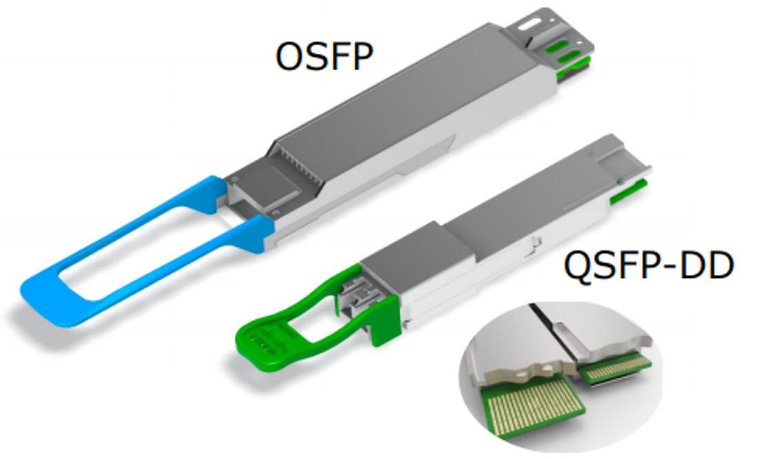
OSFP has 8 lanes in two different configurations, 50 Gb/sec per lane for a total of 400 Gb/sec and 100 Gb/sec per lane for a total of 800 Gb/sec. It’s larger than QSFP-DD and measures 22.58
OPTICAL MODULES 19 DESIGN WORLD — EE NETWORK 05 • 2024 eeworldonline.com | designworldonline.com
Figure 1. Common SPF form factors, SPF28 is an enhanced version of SPF+ in the same mechanical configuration.
x 107.8 x and 13.0 mm compared with 18.35 x 89.4 x 8.5 mm for QSFP-DD. A 1U front panel can accommodate up to 36 OSFP ports for a total of 14.2Tb/sec. There are currently three single-mode fiber implementations that can support distances up to 2 km and three multi-mode fiber implementations that support distances up to 10 km. Since QSFP-DD modules are smaller their thermal capacity is only 7 W to 12 W. The larger OSFP transceivers have a thermal capacity of 12 W to 15 W (Figure 2).


Conclusion
There’s a wide range of SFP form factors that support an equally wide range of speeds and applications. SFP is not an official standard, it’s supported by an MSA that can result in some differences between modules from various vendors. In addition, while it’s mostly associated with optical transport, copper is also an option in some installations.
References
QSFP-DD vs OSFP vs QSFP56 vs QSFP, Fiber Mall
Quickview about SFP, SFP+, SFP28, QSFP+, QSFP28, QSFP-DD and OSFP, LightOptics
SFP vs SFP+ vs SFP28 vs QSFP+ vs QSFP28, What Are the Differences?, FS
Figure 2. OSFP uses a larger module with more thermal capacity compared with QSFP-DD. (Image: Fiber Mall)


5G, WIRELESS, & WIRED COMMUNICATIONS HANDBOOK
EE World Online’s EE LEARNING CENTER An online technical education portal featuring content and multimedia resources focused on electronic engineering challenges. • Training Center Classrooms • Featured FAQs • EE Design Guide Library • EE World Videos + more www.eeworldonline.com/learning-center
Choose a 5G base station’s PA bias control circuit
Bias control of PAs is crucial to ensure optimum radio performance under all conditions. Current sensing and temperature sensing provide the feedback needed to control the PA bias. The choice of sensing and biasing circuits brings design trade-offs.
Ritesh Jain, Pratik Kalyanasundaram, and Himanshu Khatri, Renesas Electronics
5G
base station power amplifiers (PAs) need biasing using a separate bias controller to maintain optimum performance over temperature. When designing a PA bias circuit, you can use current sensing with open-loop control or temperature feedback for closedloop control. Each has advantages and disadvantages.
PAs play a crucial role in delivering RF power to a base station's antenna. Average power for 5G can range from 2 W to 15 W, with peak power ranging from 16 W to 120 W. PAs must maintain linearity and efficiency over varying ambient temperatures as per the mission profile. Because PA bias current is a function of temperature, a PA needs bias-control circuitry to monitor and adjust the PA bias in response to temperature changes. Unlike handset PAs, an envelopetracking-based adaptive biasing scheme may not be optimal owing to the higher RF power.
Figure 1 shows a typical block diagram of a PA and its bias controller in a transmit chain. The bias controller can be a separate package or integrated within the PA module. It operates by sensing the PA bias and adjusting it according to predefined control logic. We will explain the functionality and design

challenges of the bias controller’s three main sub-components: the adjustable bias generation, the bias monitoring, and the control logic.
Adjustable bias generation
First, let’s describe PA biasing with an adjustable gate voltage. To deliver more than 40 dBm (10 W) output power, the circuit needs a high breakdown transistor. This helps to reduce the bias current with a reasonable device size, and it offers broadband input and output matches. Gallium-Nitride (GaN) devices are a popular choice because they typically operate at 28 V to 48 V drain voltage and provide good RF amplification and power-transfer efficiency. Other popular choices for lower power outputs are Gallium-Arsenide
Figure 1. This block diagram of a transmitter chain showsa PA module and bias controller with major subcomponents.
(GaAs) and laterally diffused metal-oxidesemiconductor (LDMOS).
These technologies are, however, expensive, offer lower levels of integration, and suffer from process variations as compared to their silicon counterparts. Under optimal biasing for amplification, the drain current of a transistor is, typically, a polynomial or an exponential function of its gate voltage (we use the general terms "gate" and "drain" even for bipolar transistors where the equivalent terminals are "base" and "collector," respectively). This makes the bias current highly sensitive to gate voltage variations while it exhibits a weak dependence on the drain voltage. In many applications, the gate voltage is typically generated using current-mirror circuits that are themselves driven by
21 DESIGN WORLD — EE NETWORK 05 • 2024 eeworldonline.com | designworldonline.com POWER AMPLIFIERS

precise supply-independent current sources. Furthermore, these current sources may have precise temperature slopes that can help achieve optimal performance over the operating temperature range. Typically, a high-precision digital-to-analog converter (DAC), controlled by the baseband processor, generates the gate voltage.
High die costs, large devices, poor level of integration, device mismatches, and part-to-part variations, however, make this approach impractical for typical base station PA devices based on GaN, GaAs, and LDMOS technologies. Instead, it is advantageous to have a separate bias-controller chip implemented in a silicon-based technology that not only addresses many of these concerns, but offers robust digital integration.
The next important parameter is the DAC output voltage range, which depends
on the transistor technology used in the PA. Table 1 outlines the gate bias voltage ranges for some of the popular technologies.
A driver amplifier typically precedes the power amplifier. Many base-station implementations use different technologies for the PA and driver amplifier. For instance, the PA device may be a GaN transistor, while the driver amplifier may be a GaAs HBT or LDMOS device. Thus, the bias controller DAC needs both positive and negative voltage ranges. It also needs to handle a relatively large voltage while offering low-power transistors for compact digital implementation. Hence, a bipolar-CMOS-DMOS (BCDMOS) process that can handle large dual-rail output voltages and allows for digital system integration on the same die is a popular choice. Modern BCDMOS processes are based on the relatively low-cost and
readily available legacy 180 nm or 130 nm CMOS process nodes. The DAC resolution is also an important design parameter because it determines the bias precision. Here, most of the products on the market provide 12-bit DAC as standard, which leads to 1.2 mV and 2.4 mV bias resolution for 5 V and 10 V voltage-range, respectively. Designers should also consider that the PA transistor remains in an off state before the circuit applies the drain bias. That's especially important for depletion-mode HEMT devices that are fully on at zero gate bias and require an active turn-off (Table 1). Bias controllers also integrate a sequencing logic through a PA enable line that they assert through the powergood logic of the drain supply generator only after asserting the drain voltage. Also, for the depletion HEMTs, the drain voltage should be asserted after the negative supply to ensure that the transistor is off.
PA switching and the DAC
Now, let’s revisit the PA on-off switching through this DAC output. The transmitter switching time in a 5G radio should be a maximum of 10 µsec as specified by 3GPP. The PA switching by itself needs to be much faster. The DAC output loaded with a large PA gate capacitance may, however, lead to a long settling time for the on-and-off voltages.
Table 1. Gate bias voltages for different PA transistor technologies. The exact voltages for different transistors may vary. This table provides a general idea of the voltage range applicable for that process.
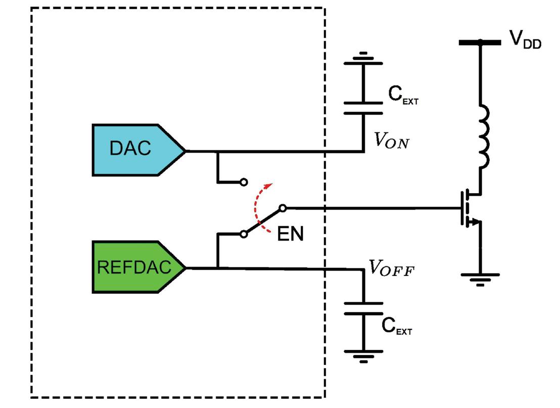
Addressing this issue requires two DACs where the main DAC generates the on voltage while the reference DAC (REFDAC) generates the off voltage. These DACs then feed the gate terminal through an SPDT switch, shown in Figure 2. Large capacitors, typically 10 times the gate bias capacitor, further stabilize the voltage and act as charge reservoirs to assist in the rapid switching.
Modern high-efficiency base transceiver station (BTS) PAs use the Doherty architecture having two transistors per stage. Commercial PA modules may integrate the driver and the final stage within a single package, thus doubling the number of transistors. One PA may require up to four DAC channels for its bias control. Multiple gates may share the reference DAC that generates the off voltage, while the on voltage may differ based on the transistor operation class. Now, modern massive-MIMO (mMIMO) radios may have 64 transmit channels, thus requiring 256 biasing channels. Integrating multiple channels within a package can reduce the bill-of-materials (BOM) and routing complexities. This is also an engineering challenge owing to the die size and thermal constraints.
Bias monitoring
Recall our original problem statement: the PA bias current
Figure 2. Rapid PA switching using an SPDT switch (EN signal) with two DACs generates ON and OFF voltages separately, each stored in external capacitors CEXT
5G, WIRELESS, & WIRED COMMUNICATIONS HANDBOOK 22 DESIGN WORLD — EE NETWORK 05 • 2024 eeworldonline.com | designworldonline.com
is a function of temperature. We need to sense this variation to determine when and how much bias control the PA needs. This is accomplished by directly sensing the bias current and then adjusting the PA bias constant level, thus forming a closedloop control. Another way is to sense the PA temperature and provide a bias voltage based on a predetermined look-up table. Hence, this method is an open-loop control. Each control method brings with it different challenges.
Figure 3 shows the current sensing for the closed-loop control. Here, we place a small external sense resistor between the supply and the choke inductor. Doing so results in a proportional voltage drop amplified with a current-sense amplifier and digitized with an analog-to-digital converter (ADC). This voltage is a direct measure of the current. Note that this voltage drop must be very small because it also reduces the PA voltage headroom, which directly impacts the output power and degrades the efficiency. For a 0.1 V drop with up to 1 A of bias current, a 100 mΩ sense resistor may be used. A 1 mA current sensing resolution implies a 100 μV voltage resolution for this readout, which is an extremely challenging precision to achieve given the supply voltage of 5V to 48 V and the presence of direct and coupled noise.
Therefore, such a sensor must have low noise performance, high gain, and a high common-mode rejection ratio (CMRR), along with proper decoupling and shielding. The sense nodes should also have a strong ESD rating and handle a voltage of 48 V.
Figure 4 shows the temperature sense in the open-
loop control. Use an external temperature sensor, which could be a diode, positioned close to the PA. This sensor gets its power from the bias controller and the resulting output voltage goes to an ADC.
Based on the temperature reading, the control logic may bias the PA according to a predetermined look-up table (LUT). You can automate this process where the circuit periodically measures the temperature and updates the PA bias voltage. This may be a simpler arrangement than the current-sensing method, though it comes with its own obstacles.
First, this method may not allow a precise control of the PA bias. The temperature variation at the sensor depends on its placement and proximity relative to the PA hotspots (Figure 4). The sensor may see a reduced temperature variation, which can impact the biasing precision. As the temperature is only an indirect measure of the bias current, careful calibration is needed to map the two parameters. On the other hand, temperature-based biasing can be used for all the devices, while the current sensor may be implemented on the supply of the main device only. In either of the schemes, the bias controller die should also have an internal temperature sensor to account for any local temperature variations.
Control logic
The control logic adjusts the bias voltage based on the sensed current or temperature. This control logic can't be hardcoded; it must be programmable to account for the PA's process variations. This is one reason why an analog auto-control can't be used for the closedcontrolx. The control logic may


be implemented in an integrated microprocessor, though this is often overkill. An optimum solution is to program the logic in the BTS host controller, which then configures the bias controller through a digital interface such as I2C or SPI (see Figure 1). This may enable radio manufacturers and operators to optimize the control logic based on their mission constraints.
Specifically for open-loop control, a look-up table (LUT) is sometimes integrated within the bias controller's nonvolatile memory to map the temperature to the required PA bias, which reduces the load on the host controller. In such implementations, the LUT may also integrate interpolation logic and an autonomous control mode based on the LUT map.
Summary
While the essential bias-control principle remains the same, there are myriad ways that differ in their implementation details and thus require careful consideration from the system perspective. For the system integration, it is important to understand the bias controller features and their associated trade-offs across the three discussed subcomponents to select the best applicable solution. It is equally important for the IC designers to understand the different challenges and the overall system before designing these solutions.
Figure 3. Current sensing-based closed loop bias control of a PA transistor.
23 DESIGN WORLD — EE NETWORK 05 • 2024 eeworldonline.com | designworldonline.com POWER AMPLIFIERS
Figure 4. The external bipolar transistor functions as a temperature sensor, used for open-loop bias control of a PA.
How to reduce residual noise in 5G NR EVM measurements
Error vector magnitude (EVM) is the most important figure of merit for signal quality in 5G NR. A new method improves measurement accuracy by reducing noise.
Paul Desinowski, Rohde & Schwarz
EACH
new generation of cellular technology increases end-user throughput or bit rate over previous generations. Each new generation accomplished higher data rates through a combination of both wider channel bandwidths and higher-order modulation. Even when we compare LTE and 5G New Radio (NR) with equal channel bandwidth, 5G NR delivers higher throughput through higherorder modulation. Unfortunately, higher-order modulation makes receivers more sensitive to noise and thus bit errors. The good news is you can compensate for the noise in your test equipment.
Both LTE and 5G NR modulate their signal carriers (or rather, subcarriers) using quadrature amplitude modulation (QAM). QAM conveys information by changing the carrier's amplitude and phase between different states or “symbols.” A symbol is a unique combination of amplitude and phase. The number of symbols means the number of bits transmitted with each symbol. For example, a modulation scheme that has 16 symbols can encode 4 bits per symbol, whereas a system using 256 symbols can convey 8 bits per symbol.
A constellation diagram shows the modulation, where each symbol is the endpoint of a vector having a given magnitude and phase. Modulation order is simply the number of possible symbols. The 16QAM constellation shown in Figure 1 has 16 symbols or vector endpoints.
In practice, a signal's amplitudes and phase shifts don't precisely fall on the defined symbol endpoints. The error may be due to magnitude error, phase error, or, most commonly, a combination of both. Should an amplitude and phase combination deviate too far from the ideal point, the receiver could incorrectly decode it, which leads to bit errors.

Figure 1. A 16QAM constellation diagram shows sixteen combinations of amplitude and phase. Each point represents four bits, and the distance from the center to each point is the vector.

Figure 2. The difference between an amplitude and phase point and its ideal location represents an error vector.
24 DESIGN WORLD — EE NETWORK 05 • 2024 eeworldonline.com | designworldonline.com 5G, WIRELESS, & WIRED COMMUNICATIONS HANDBOOK
EVM defined
You can find the difference between ideal and measured symbols by connecting these two points with an error vector (Figure 2). Like all vectors, this vector has a magnitude and a direction. In most cases, the error magnitude, rather than its direction, matters. Therefore, modulation accuracy is quantified as the error-vector magnitude (EVM). Larger values of EVM mean greater distance between the measured and reference points and thus a higher probability of bit errors.
A signal analyzer calculates EVM at each symbol time and reports it as a normalized quantity, either relative to the maximum power or to the RMS power in the received signal constellation. Most standards use RMS, but you must verify the method when comparing EVM values. EVM uses units of percent or dB, usually as statistical values (mean, max, min, etc.) over some period. Analyzers may also plot EVM for successive symbols to see whether EVM remains constant during a transmission. Lower values of EVM, that is, smaller percentage values or lower (more negative) dB values, are always more desirable than greater values. Typical EVM values for 5G NR networks typically run -40 dB to -50 dB or single-digit percent values.
The importance of good EVM increases as the modulation order increases. In higher-order modulation, such as OFDMA, where the symbols or constellation points are close together, errors in the received signal's magnitude and/or phase are more likely to lead to incorrectly decoded symbols because the

4. This EVM measurement setup uses a vector-signal generator and spectrum analyzer to measure EVM in a device under test.
symbols are close together. Figure 3 shows constellation diagrams for 16 QAM, 64 QAM, and 256 QAM.
5G NR achieves higher throughput in part by using higher-order QAM modulation, in particular 64 QAM and 256 QAM. These modulations do, however, require both better performance at the transmitter and receiver, as well as a “cleaner” RF environment than 16QAM. Like many other wireless standards, 5G NR places limits on the maximum permissible EVM, which decreases as modulation order increases. In 5G NR, 16 QAM requires an EVM of no greater than 12.5%, while 256 QAM requires an EVM of 3.5% or less.
Because EVM is the primary “figure of merit” for modulation quality in 5G NR networks, you must accurately and repeatably measure a device's or system's EVM. Use a spectrum analyzer or signal analyzer to make EVM measurements. These instruments can decode the received 5G NR signal and calculate its EVM. In some test scenarios, you need a vector-signal generator to create a modulated 5G NR signal, which serves as the input to a device under test, such as a power amplifier, as shown in Figure 4.

Get the actual EVM
When measuring EVM, remember that the measured EVM is a combination of both the EVM of the device under test (and potentially the channel) and the EVM created by or within the measuring instrument. The contribution of the analyzer to overall EVM is sometimes referred to as residual EVM. Traditionally, the requirement for accurate EVM measurements was that the measuring instrument should have an EVM that was at least 10 dB better than the DUT's EVM. Unfortunately, even with high-performance instruments, this margin can be difficult to obtain. The fact that you must make some 5G NR measurements over-the-air rather than in a conducted test environment further increases the need for good analyzer EVM performance, especially with low signal levels due to free-space path loss or other factors.
An analyzer's residual EVM has four primary sources:
• phase noise,
• frequency response,
• nonlinearities, and
• wideband noise.
The first three are relatively easy to address. Using high-quality local oscillators, high-performance spectrum analyzers can limit the contribution of phase noise to residual EVM. You can calibrate out or compensate for the effects of frequency response, the variation in received-signal characteristics as a function of frequency.
Figure 3. As order modulations (16 QAM, 64 QAM, and 256 QAM) increase, the vector points on a constellation diagram get closer.
25 DESIGN WORLD — EE NETWORK 05 • 2024 eeworldonline.com | designworldonline.com EVM MEASUREMENT
Figure
Figure 5. Improvement in residual EVM using IQ noise cancellation (IQNC) occurs as a function of attenuation and number of captures.
Attenuation addresses nonlinearities such as harmonics and intermodulation products by limiting a received signal's amplitude, which avoids compression within the analyzer.
Wideband noise is, however, a more challenging issue in EVM measurements. This noise is normally characterized using traditional noise-figure measurements. It includes both thermal noise and noise contributions from individual components. Furthermore, this noise scales with bandwidth, meaning that wideband noise is an even greater issue given the wider bandwidth signals commonly used in 5G NR. Because 5G NR often requires the measurement of signals having a wide bandwidth, accurate EVM measurements for 5G NR devices require some method of reducing or mitigating the impact of wideband noise on residual EVM.
Noise reduction methods
Various methods can remove or reduce analyzer-added noise. IQ noise cancellation has emerged as the most promising method. Depending on the amount of input attenuation, IQ noise cancellation can improve EVM measurement performance by approximately 5 dB, a significant improvement when measuring EVM in 5G NR networks.
Performing an IQ noise cancellation procedure requires several measurements. Figure 5 shows the additive effect from noise sources.
1. Make a measurement containing all noise contributions, both internal and external.
2 Make a measurement with the analyzer input terminated to find the noise contribution of the analyzer alone.
3. Make multiple captures on the signal to estimate an ideal, noise-free capture.

Make the measurements on raw IQ data, that is, on the digital representation of the received signals. This method reduces the contribution of wideband noise to residual EVM better than other methods for several reasons.
• IQ noise cancellation requires a single measurement path in the measuring instrument. It can be performed entirely in software and implemented without requiring a hardware change.
• IQ noise cancellation is also independent of the modulation type or order.
• IQ noise cancellation won't cancel out noise from the signal generator noise or from the DUT.
Conclusion
EVM continues to be the most important figure of merit for modulation quality in wireless networks. It quantifies the distance
between the ideal constellation or symbol points and the actual received or measured symbol points. Lower values of EVM (expressed in units of percent or dB) are always desirable. Many standards, including 5G NR standards, specify a required maximum EVM level for a given modulation order.
EVM is normally measured with a signal analyzer or spectrum analyzer. Although this measurement is well understood and has been used in previous generations of cellular technology, EVM measurements are particularly important in 5G NR due to higher modulation orders and wider bandwidths. Accurate EVM measurements of 5G NR signals are, however, challenging. Fortunately, recent developments such as IQ noise cancellation let existing instruments make reliable and repeatable EVM measurements and thus verify compliance with relevant 5G NR modulation quality requirements.
26 DESIGN WORLD — EE NETWORK 05 • 2024 eeworldonline.com | designworldonline.com
5G, WIRELESS, & WIRED COMMUNICATIONS HANDBOOK
Wi-Fi performance testing now has standards
Until recently, service providers were unable to predict in-home performance of Wi-Fi devices because they lacked standardized test cases. Now, industry groups have advanced three new standards, each geared toward different Wi-Fi use cases. Leigh Chinitz, Spirent Communications
THEWi-Fi industry has long had standardized conformance testing to confirm that a device conforms with standards and will interoperate with other Wi-Fi-certified devices. Until recently, though, there was no standardized way to measure Wi-Fi performance or make comparisons across devices. For service providers, this lack of industrywide, vendor-agnostic performance testing has been an ongoing source of frustration.
According to one study, 92% of U.S. households use Wi-Fi for home Internet, and more than 25% of those surveyed value quality of experience (QoE) over price [1]. Given that many subscribers rely on Wi-Fi routers or gateways provided by their service provider, operators get the blame — and support calls — when customers have a bad experience. Providers want as much information as possible when evaluating equipment to deploy to their customers. Service providers have been among the loudest voices advocating for standardized performance testing.
Why has it taken so long for the industry to respond? The answer is a story in itself, though one with a happy ending: There are now three different standardized test sets available, each examining different aspects of WiFi performance in different contexts. As Wi-Fi technology grows more
sophisticated with each new release, and more important to both residential and business users, these efforts couldn’t have come at a better time.
Why so hard?
Conformance testing and performance testing are different. Think of it this way: “Will this device interoperate with that device?” as opposed to “How well will this device perform while interoperating with that device?” Both questions are important, and industry efforts to answer the first have been enormously consequential. The fact that you can buy any Wi-Fi-enabled smart TV, for example, without worrying if it will work with your home router, is a testament to the Wi-Fi Alliance’s conformance testing regime. Arguably, the confidence consumers have that Wi-Fi devices will interoperate is the biggest reason for WiFi’s global success. Performance testing is, however,
another matter. There are, of course, methods to measure how a device performs in each location, but they typically require RF experts to conduct onsite walk tests with specialized equipment. Such tests are useful when outfitting a new enterprise campus but not scalable to millions of subscriber homes. Figure 1 shows just one of countless possible configurations. Coming up with a standardized test set that can be conducted in the lab for this purpose — that will yield consistent data
to
WIRELESS PERFORMANCE 27 DESIGN WORLD — EE NETWORK 05 • 2024 eeworldonline.com | designworldonline.com
Figure 1. Wi-Fi performance testing standards address how well Wi-Fi works in a home setting.
make meaningful comparisons — has proven much more difficult for several reasons.
First, Wi-Fi performance is extremely sensitive to environmental factors. A location’s layout, construction materials, and, especially, other devices sharing its RF airspace can all affect performance. Even in the same location, airspace is highly dynamic, so the same test set can yield different results from one hour to the next. A device’s performance can also fluctuate depending on the types of traffic different devices are transmitting and the specific interference conditions at that moment — factors that are difficult to recreate or control in the lab.
With so much variability, Wi-Fi access point (AP) vendors have been skeptical of any attempt to define testing standards that would rank one device’s performance over another in a purportedly objective way. It’s hard to blame them. We don’t even have a universally accepted definition of what “good Wi-Fi performance” means. What a given customer considers good represents a mix of data rates, range, reliability, supported features, and price. A device that’s an excellent choice for one use case (say, home broadband) might be poorly suited to another (a busy office
environment), and vice-versa.
Use-case testing
If navigating Wi-Fi variability has been the biggest challenge in developing standardized performance testing, embracing that variability has enabled us to finally find a solution. Rather than trying to devise a single, universal test set to compare devices, the industry has adopted a “fit for purpose” approach, advancing three different standards to measure performance for specific Wi-Fi use cases. They are:
• Broadband Forum (BBF) TR-398: Released in 2019, BBF’s Wi-Fi InPremises Performance Testing plan was the first to define specific performance test cases and methodologies for evaluating residential Wi-Fi. True to the fit-for-purpose model, TR-398 focuses exclusively on residential APs (not client devices), measuring in-premises performance in singleAP environments, which is the most common home deployment [2].
The test plan covers RF capability, coverage, stability, and performance, both at baseline and with multiple connected clients, with pass/fail criteria for each test [3].
• Wi-Fi Alliance Device Metrics Test
Figure 2. Performance testing addresses the tradeoff among capacity, latency, throughput, and coverage.
Plan: This 2022 effort from Wi-Fi Alliance’s Customer Experience Group is also geared towards residential Wi-Fi APs. Instead of establishing baseline pass/fail performance tests, however, the Device Metrics Test Plan aims to provide consistent statistical analysis so that testers can compare devices for a specific purpose. Test cases include rate vs. range, AP latency, channel switching, roaming, and augmented reality/virtual reality (AR/VR) performance. The standard focuses on analyzing and presenting data in a clear and consistent way so that prospective buyers can decide for themselves, based on their specific market and end-user requirements, whether a device meets their needs.
• European Telecommunications Standards Institute (ETSI) specification TS 103 754: Also released in 2022, the ETSI Broadband Radio Access Network (BRAN) Multiple Access Points Performance Testing Plan provides a framework specifically for evaluating multi-AP environments, such as Wi-Fi mesh or extender scenarios [4]. It covers roaming time and throughput, one- and two-hop throughput, band steering, and network configuration and self-healing.
While focusing on different use cases, these standards share some commonalities. They all require that tests be conducted in a controlled RF environment (not open air) and that testers use multiple independent, interconnected RF chambers (at least for some of the test cases) to create more complicated and lifelike testing topologies.
New features, new challenges
The release of these standards is good news for service providers and Wi-Fi customers. For the industry groups advancing them, however, the work is only beginning. As useful as these initial test cases are, they still provide only a partial picture of Wi-Fi performance. They don’t address several of
5G, WIRELESS, & WIRED COMMUNICATIONS HANDBOOK 28 DESIGN WORLD — EE NETWORK 05 • 2024 eeworldonline.com | designworldonline.com
the more advanced features in Wi-Fi 6 or Wi-Fi 7, and new features are constantly in development.
In many cases, new Wi-Fi capabilities expand not only the way we define “good performance,” they create new use-case-specific testing considerations. Consider two features introduced in Wi-Fi 6: Multi-user orthogonal frequency-division multiple access (OFDMA) adds new channel and multi-user capabilities, including allowing an AP to communicate with multiple end devices simultaneously [5]. BBF’s TR-398 Issue 2 added some new testing focused on the Wi-Fi 6’s higher throughput, but the standard does not yet address OFDMA performance.
Targeted Wake Time (TWT) enables more flexible sleep time options for Wi-Fi devices. So far, we lack a test to measure this performance — or any other Wi-Fi power-saving features.
As Wi-Fi becomes more important for a wider range of devices and applications, the need to understand how these features perform will grow. For instance, Wi-Fi devices will increasingly use OFDMA to improve throughput and quality for streaming and realtime videoconferencing. Power-saving features such as TWT will connect door locks, alarm systems, home appliances, and other IoT devices. Service providers will need to test device performance with and without these features and under different conditions while sharing a network with other devices. Figure 2 compares capacity, latency, throughput, and coverage parameters and where testing services and technologies fall.
Fortunately, the groups that developed the first wave of performance testing standards continue to expand them. For example, TRF-398 Issue 2 added dual-band and bidirectional throughput tests, channel auto-selection tests, and initial “roaming” and “repeater” tests. Issue 3, which BBF will release in 2024, will add testing to address the new 6-GHz spectrum, quality of service (QoS), latency, and more.
Looking ahead
With the release of Wi-Fi 7, we can expect even more advanced features and more complex testing challenges. Changes to Wi-Fi modulations, new OFDMA spectrum-allocation functions, and especially multi-link operation (MLO), which enables APs to combine channels across bands, promise to dramatically improve throughput and QoE for end-users.
Defining use cases, test methodologies, and metrics for these new features will be a major area of focus moving forward. Equally important, as customers use Wi-Fi to support more mission-critical applications in both homes and businesses (a primary area of focus for Wi-Fi 7), we will need the ability to measure and guarantee performance in more granular ways.
The good news is that we finally have an approach to Wi-Fi performance testing that everyone can agree on. By adopting fit-for-purpose testing, we can sidestep the challenge of creating a single, universal standard for measuring performance. Instead, we can provide something much more useful: clear data for the use cases that matter most to each customer.
References
1. Erik Gruenwedel, Parks: 92% of U.S. Internet Households Use WiFi at Home, Media Play News, January 2023, 2023. https://www. mediaplaynews.com/parks-92-percent-of-us-internet-householdsuse-wi-fi-at-home/
2. TR-398, Wi-Fi Residential & SOHO Performance Testing, Broadband Forum Technical report, Issue 3: March 2024. TR-398
3. Wi-Fi Tutorial Lesson 6: TR-398, Spirent Communications https:// www.spirent.com/assets/u/video-wi-fi-tutorial-lesson-6-tr-398.
4. ETSI TS 103 754 V1.1.1 (2022-06), Broadband Radio Access Networks (BRAN); Multiple Access Points Performance Testing, https://www.etsi.org/deliver/etsi_ts/103700_103799/103754/01.01. 01_60/ts_103754v010101p.pdf.
5. Bob Witte, OFDMA improves spectrum use in Wi-Fi 6, 5G Technology World, June 4, 2020. https://www.5gtechnologyworld. com/ofdma-improves-spectrum-use-in-wi-fi-6/
29 DESIGN WORLD — EE NETWORK 05 • 2024 eeworldonline.com | designworldonline.com WIRELESS PERFORMANCE
mmWaves bring challenges to 5G and 6G
Signals in the mmWave range require extra care and more expensive components than at sub-6 GHz frequencies. Roger Kauffman, Molex
DATAdemands keep pushing for more bandwidth in wireless networks, and this trend will surely continue. AI, autonomous vehicles, AR/VR, and other technologies will see to that. The mmWave spectrum allocated for 5G can meet the bandwidth needs, but not without economic and technical tradeoffs.
The benefits of mmWave revolve around its capacity. This spectrum, from roughly 30 GHz to 300 GHz (5G mmWave starts at 24 GHz), offers thousands of megahertz of bandwidth compared to sub-6 GHz 5G, which has hundreds of megahertz. Even so, the wireless industry is considering frequencies up to 100 GHz for 5G, with 6G research looking into 140 GHz and beyond. These frequencies bring technical challenges in terms of signal losses in connectors, cables, PCB traces, and over the air.
Propagation, or a signal's ability to travel through a medium, differs significantly between sub-6 GHz 5G and mmWave frequencies. As Figure 1 shows, mmWave signals have a limited or diminished ability to pass through buildings, trees, rain, and other objects between a transmitter and receiver. Repeaters and small cells can mitigate those issues.

Figure 1. Trees, glass, buildings, walls, rain, and most other things block mmWave signals. At these frequencies, direct line-of-sight makes all the difference.
In addition, mmWave radios use massive MIMO antennas with beam steering to increase efficiency and at much lower transmit power levels than omnidirectional antennas. The short range of mmWave signals means that radios may need to be located every 1,000 meters, as opposed to sub-6 GHz radios, which can be several kilometers apart. This is one element of the cost that network operators face.
Design challenges of mmWave
Designing a mmWave radio brings other challenges. As the frequencies increase, mmWave components, PCB materials, PCB traces, and interconnects that minimize signal loss costs more than those designed for lower frequencies.
For this, consider the coaxial connectors shown in Figure 2. The common SMA connector can work to 18 GHz.
At mmWave frequencies, RF connectors need smaller sizes to efficiently carry the signal. When moving to mmWave, you might use a 2.92 mm connector that can work to 40 GHz. Unfortunately, mechanical tolerances of the inner components within the connector must be more stringent than for SMA connectors. These tighter tolerances can be two-to-three times more costly than ones used in systems operating under 10 GHz.
In a 5G sub-6 GHz radio system, board-to-board RF coaxial connectors often route RF signals between the power amplifier board, filter, and antenna.
30 DESIGN WORLD — EE NETWORK 05 • 2024 eeworldonline.com | designworldonline.com 5G, WIRELESS, & WIRED COMMUNICATIONS HANDBOOK
As the number of transmit channels increases, engineers prefer the three-piece connections shown in Figure 3 to achieve axial and radial alignment during assembly.
For an active massive MIMO antenna system with 64 transmit channels, this would equate to at least 64 RF boardto-board sets per radio. Some massive MIMO active antenna systems have 128 transmit/128 receive channels or more. If the RF connector three-piece solution is an average of $0.60 per set, this suggests the connector content of the active antenna/ radio could be more than $150.
EMI and crosstalk
High-frequency signals pose additional challenges for connector and cable designs. Using the massive MIMO example, with RF coaxial systems located near one another, you must minimize EMI and crosstalk. Shielding becomes more critical on separable interfaces (coaxial connectors) or, if used, coaxial cables. Many RF board-to-board connectors use slotted outer ground conductors that let them slide or snap together when mated.

The design of these slots and any potential openings with axial misalignment must be carefully managed to minimize EMI.
Signal attenuation presents another challenge. As channel numbers increase, the output power per channel typically decreases. That decreased output power increases the need for low-attenuation RF transmission paths (such as boardto-board connector systems). Many connectors found in sub-6 GHz applications use molded dielectric materials as a compromise between signal attenuation and cost. Because attenuation increases with frequency, most molded dielectric materials used in RF connectors aren't efficient enough for mmWave radio systems. RF connectors that operate to 100 GHz and higher typically use air as the primary dielectric. The center conductors are supported by small,

molded support beads. Some connectors, like SMP or SMPM (Figure 4), have polytetrafluoroethylene (PTFE) dielectric materials and may be a reasonable compromise.
PCB materials also pass RF signals within radios. There are similar considerations for PCB materials and construction of the RF coaxial challenges mentioned above. Low-loss PCB materials are available today, but these carry a premium compared to materials used in sub-6 gigahertz systems. EMI and crosstalk tend to be managed using multiple-layer PCBs, vias, and other isolation techniques. 5G massive MIMO antennas that cover mmWave frequencies between 22 GHz and 39 GHz may use ten or more PCB layers to achieve reasonable performance. Considering the moderate output power per channel and the effects of beam steering of massive MIMO signals, achieving the desired effective isotropic radiated power (EIRP) of the system can be difficult.
What about 6G?
In 6G, mmWave radio systems that may play a role include a range of products from dielectric waveguides to molded antennas. These technologies direct the incident angle of the beam toward the user, which minimizes EIRP reduction in beam steering. Work on digital beam steering devices and other technologies continues to enhance mmWave radio performance. Coaxial
31 DESIGN WORLD — EE NETWORK 05 • 2024 eeworldonline.com | designworldonline.com MMWAVE CONNECTIONS
Figure 2. Higher frequencies reduce connector size, but manufacturing tolerances also shrink, making them more expensive.
Figure 3. Increased frequency makes connectors shorter and denser.
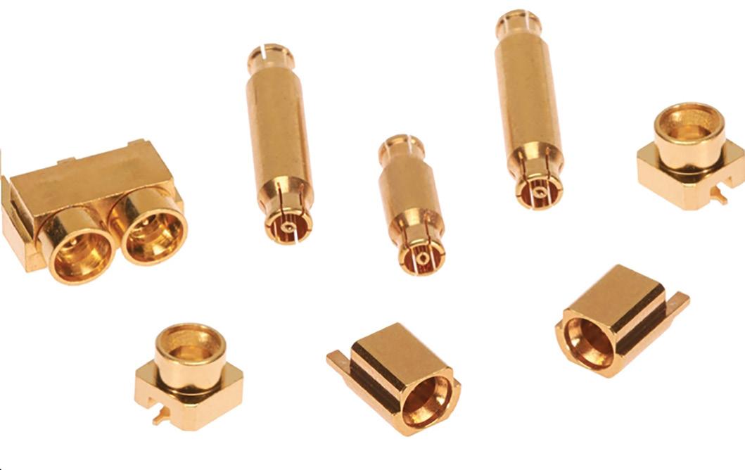
connectors that operate up to 145 GHz are now available should 6G move into the terahertz frequency spectrum.
As 6G research continues, frequencies between 6.4 GHz and 15 GHz are also being considered. This may suggest that 6G will adopt some of the lessons learned in 5G RAN deployment strategies, leaning on a lower frequency spectrum.
At this time, we still don’t know how 6G will differ from 5G or 5G-Advanced. Millimeter-wave frequencies have much greater bandwidth than sub 6 gigahertz signals, roughly 1.2 GHz versus
less than 600 MHz. How will systems be developed and deployed that make economic sense for the wireless network operators? As the theoretical use cases take time to develop, will 6G be a compromise that finds the most benefit from the spectrum from 7 GHz to 15 GHz? Perhaps AI, autonomous vehicles, VR, and the expansion of fixed wireless access (FWA) will drive the industry toward greater use of the mmWave spectrum. It’s possible that by 2035, we will all want to holographic calls for meetings instead of video conferencing. Considering how we used our mobile devices during the 2G/3G era as compared to today, it’s clear we’ve come a long way.
There must be a new use case or application in the nottoo-distant future that will continue to drive the need for greater bandwidth. Because many of the wireless network operators already have ownership of this valuable spectrum, they will be happy to make it available so long as the economics make sense.

design guide on Bluetooth & Connectivity
The demand for high data throughput, low power, and longer battery life is driving much of the breakthroughs and evolutions in connectivity technology.
In this Design Guide, we present the need-to-know basics, as well as the technology fine points aimed at helping you and your designs keep pace and stay competitive in the fast-changing world of connectivity.
5G, WIRELESS, & WIRED COMMUNICATIONS HANDBOOK
Figure 4. SMP connectors handle frequencies up to 40 GHz.
BROUGHT TO YOU BY: find this design guide and more in EE WORLD’S learning center: www.eeworldonline.com
Build a 5G Open RAN test lab with open-source software tools
Open-source software provides network components that you can use to simulate 5G network functions from the network core to the radio.
Lincoln Lavoie, University of New Hampshire Interoperability Lab
DEVELOPING
and deploying a laboratory infrastructure to support testing 5G and open radio-access network (Open RAN) systems can present a daunting and complex task. Prior to Open RAN, this task was only possible by engaging directly with the large network system vendors. Since then, several open-source projects and organizations have developed materials based on 3GPP and O-RAN Alliance specifications. Those tools and resources make it possible to create a complete 5G deployment, spanning from the mobile core to RAN, providing invaluable resources for engineers.
Open-source activities play an important role because they enable rapid prototyping and verification of the specifications. Those specifications could still be in draft form. Many standardization groups have devised practices and policies to promote the use of open source. These groups include the Internet Engineering Task Force (IETF), guidelines and practices around “rough consensus and running code,” and the Open Software Community (OSC) of the O-RAN Alliance, which have implemented formal programs.
Indeed, one of the most complex aspects involving opensource projects and components in a 5G test lab is where
to begin. In this article, we will discuss some fundamental components that engineers can use as starting blocks and explain how open-source software can support Open RAN testing.
To begin the process, you need to first understand some of the major components of a 5G network. In this case, we will generalize the core network as a single component, as multiple open-source options currently implement the core network functions required by 3GPP specifications. The 5G mobile core comprises various individual network functions that enable the services-based architecture defined by 3GPP.
Three well-known examples of open-source systems implementing the 5G core are the Open 5GS project, the free 5GC project, and the Open Air Interface 5G core network component (Ref. 1, 2, 3). The former two projects are standalone implementations of the 5G core. The latter is more tightly coupled with the larger Open Air Interface (OAI) project, which can also provide the RAN.
At UNH-IOL, we frequently use the Open 5GS core, which we deploy as two sets of components. First, we deploy the primary control components, including the access and mobility management function (AMF), 5G session management function

TEST LABS 33 DESIGN WORLD — EE NETWORK 05 • 2024 eeworldonline.com | designworldonline.com
Figure 1. The UNH-IOL has deployed this Open 5GS topology for interoperability testing of 5G network components.
(SMF), and others. Second, we deploy the user plane function (UPF), which is responsible for forwarding subscriber traffic from the RAN interfaces to the data network (e.g., the Internet). This effectively enables control/user plane separation (CUPS), with these functions deployed across separate virtual machines. Similarly, we could also implement multiple UPF instances in larger deployments to load balance the subscriber traffic. Figure 1 shows some of the logistics of this deployment in our lab.
From core to RAN
Once the core network is running, the next likely focus will be the RAN. Within this space, we’ll get closer to the leading edge of the open-source development efforts, depending on the directions taken within the deployment. The RAN provides an RF connection between the user equipment (UE) and the mobile core network. That's an oversimplification, but we’ll stick with that working definition without diving into some complex topics such as handovers, support of multiple cells, carrier aggregation, and so on. Here, the most significant factor in the selection processes will likely center around the radio components, for which we have two options.
First, we could deploy a softwaredefined radio (SDR) based system that leverages the Open Air Interface project to provide the software and firmware to implement the complete RAN, or more accurately, a good base station. Depending on the SDR hardware selected, it might be possible to connect RF ports directly to the antenna. With care to avoid violating any licensed spectrum, an RF connection to the UE device should be possible. On that note, a lab will also need shielded chambers or RF isolation rooms, but that’s outside the scope
of this article.
Another approach to implementing RAN follows the specifications from the O-RAN Alliance, where the gNodeB is disaggregated into discrete components: radio unit (RU), distributed unit (DU), and centralized unit (CU). In this space, the OAI project can provide some software, notably the DU and CU components, which then implement the Open Fronthaul interface (OFH) towards the RU. For the RU, selecting a product from a vendor is necessary because no open-source RUs currently exist.
To ensure the correct transmission of radio signals or frames, the DU and RU need to synchronize time and understand it well enough to support the OFH interface. Again, multiple architectures or approaches are possible, described as different configurations LLS-C1 through LLS-C4 (Ref. 4). In our lab, we're currently implementing LLS-C3, with one of the fronthaul switches serving as the IEEE-1588 grandmaster clock, which provides the timing to the RU and DU. Hardware time stamping support is required for the NIC on the DU server and the ptp4l project is used to synchronize the server clocks to the network. Figure 2 shows this configuration in the lab.
Assuming you will be using off-the-shelf UE devices such as phones, everything is ready to test, right? Well, very nearly. Thus far, a core network and a radio network have been deployed. Barring any configuration issues, the gNodeB should be registered with and connected to the core network. It should provide at least one cell on the desired 5G band for the UE to connect. The UE must authenticate with the network, which depends on the SIM card. In 5G, the authentication works "both ways," where the UE authenticates the network, and the network authenticates the UE. Without
diving through all the details, this requires the network information, i.e., some of the keys provisioned in the core network to match keys within the SIM card, thus enabling the cryptographic challenge/ response to successfully complete. It is not possible (for very good reasons) to read these key values from a SIM card.
Some SIM cards are, however, programmable, typically for testing purposes. So, the last part of the laboratory hardware is a small SIM card reader/ writer, along with the programmable SIMs. Fortunately, on the programming side, there are some open-source tools that let you program the network key values and the subscriber IDs into the SIM card, making it possible for the authentication to succeed. Tools we’ve used in the lab for this purpose are pysim and sysmo-usim-tool (Ref. 5,6).
Using open-source tools, you can bring the UE device online with a working 5G connection in the lab. All the work here only scratches the surface of the 5G network and testing possibilities. Still, you should enable a lab with open-sourced-based resources capable of supporting more advanced features with proper configuration, such as network slicing or carrier/cell aggregation, just to name a couple of possible topics.
References
Open 5GS project, https://open5gs.org/ 5GC project, https://free5gc.org/ 5G core network component https://openairinterface.org/oai-5g-corenetwork-project/ https://www.5gtechnologyworld.com/howieee-1588-synchronizes-5g-open-ran/ Pysim, https://gitea.osmocom.org/sim-card/ pysim
Sysmo-usim-tool, https://gitea.sysmocom. de/sysmocom/sysmo-usim-tool.
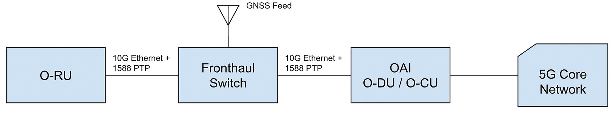
liming into account.
5G, WIRELESS, & WIRED COMMUNICATIONS HANDBOOK 34 DESIGN WORLD — EE NETWORK 05 • 2024 eeworldonline.com | designworldonline.com
Figure 2. For Open RAN, the lab uses this disaggregated topology, which takes network
How do 5G eMBB and FWA data services compare?
Fixed-wireless access is a special use case of enhanced mobile broadband, one of the three use cases specified for 5G. FWA brings different challenges for deployment than eMBB. Sridhar Bhaskaran, Rakuten Symphony

MOBILE
network operators (MNOs) are at the beginning of a wave of delivering new 5G stand-alone (SA)based data services. Where 4G has one defined data service, 5G has four core mobile data services leveraging different features of the technology.
• Ultra-Reliable Low Latency Communications (URLLC), which leverages 5G’s less than 1 ms overthe-air low latency and reliability guarantees (less than 0.001% of 20-byte packet delivery failures
after 1 ms).
• Massive Machine Type Communications (mMTC) provides connectivity for up to 1 million simultaneous IoT devices per square kilometer to support IoT sensor applications. The service features a latency of 50 ms and high reliability.
• Enhanced Mobile Broadband (eMBB) is a 5G service category that defines a minimum data transfer rate with a peak of several
Figure 1. 3GPP defines eMBB, URLLC, and mMTC, with FWA as a special use case of eMBB.
Gb/sec of download throughput and over-the-air low latency.
• Fixed Wireless Access (FWA) is a data service based on eMBB but with mobility features disabled. It is optimized for broadband wireless services for residential or enterprise applications underserved by cable or fiber-optic technologies. FWA is not defined as an explicit use case of 5G by 3GPP but is rather realized as a special case of eMBB.
Of these four services shown in Figure 1, MNOs have two 5G data services, namely FWA and eMBB, both of which are available today. Operators can roll out both services in non-standalone as well as standalone networks. URLLC and mMTC services, however, require stand-alone 5G networks and are still not fully marketready. These services are complex to deploy. You can consider them somewhat niche services compared to the broad appeal of eMBB and FWA, both of which are direct replacements and upgrades for popular consumer data services.
35 DESIGN WORLD — EE NETWORK 05 • 2024 eeworldonline.com | designworldonline.com 5G SERVICES
eMBB defined
eMBB is defined as a use case by ITU-R in IMT-2020 requirements (M.2083 specification), and the minimum performance requirements are defined in the M.2410 specification. Based on these requirements, the 3GPP specifications meet the needs of a wide range of mobile applications, including streaming of ultrahigh definition (UHD) and 8K video, virtual reality, augmented reality, cloud gaming, and business applications on the go such as video conferencing, data transfers, and cloud data updating or downloading.
To achieve these data rates, eMBB requires wide spectrum bands and specialized antenna technology, including massive multiple input, multiple output (mMIMO) antennas, and beamforming.
3GPP has defined two frequency ranges for 5G data services: FR1 (410 MHz to 7.125 GHz) and FR2 (24.25 GHz to 71.0 GHz). FR1 is commonly referred to as sub-6 GHz, and FR2 is also called millimeter wave (mmWave). The frequencies in between are called FR3, though they have not been allocated for 5G.
To reach the peak throughput requirements specified in ITU-R IMT-2020 requirements M.2410 for eMBB, FR2 frequencies are required because of their wide bandwidth. It can, however, also operate using the FR1 spectrum but with reduced peak bandwidth due to a lack of wide spectrum bands. Carrier aggregation can combine multiple noncontiguous FR1 frequency bands, thus expanding the download connection bandwidth.
While FR2 has large blocks of spectrum available for bandwidth, the transmission range of these signals is limited to 100 m to 200 m. FR2 signals degrade significantly when passing through walls or other obstructions. The use of FR2 also requires a significant expansion of the RAN infrastructure to ensure ubiquitous coverage, as well as a refresh of UE to add radios operating in the FR2 frequency bands. Energy efficiency is an important

Figure 2. In the FWA use case, CPE devices connect through routers to gNodeB base stations for internet access.
issue for network buildouts, and the use of mmWave and mMIMO technologies increases power consumption.
mMIMO is a technology that uses up to 32, 64, or 128 antennas to provide multiple streams of data between a base station and UEs. The mMIMO antenna uses phasedarray technology to enable beamforming that directs the antenna beams to areas that need bandwidth. mMIMO and beamforming provide the ability to fill in dead spots and redirect capacity as usage patterns change.
Mobility adds complexity
Deploying an eMBB service requires more signaling capacity handling than FWA and its stationary users because it needs to support hundreds or thousands of mobile users.
To handle each user's mobility, the gNodeB base station requests the UE to track and measure the signal strength of different frequencies and constantly report it. Based on that, the network decides which target frequency to hand over to users as they move from one base station to another. The event reporting thresholds for different
target frequencies are usually configurable. An eMBB service must also constantly establish and tear down the radio contexts of each UE. This connection might be longlived or only last for seconds or minutes as users check email or briefly use an app.
FWA defined
FWA provides an always-connected service from the customer premises equipment (CPE) to the 5G network core. It is suitable for residential and enterprise high-speed data services and is ideal for stationary IPTV or streaming services and VoIP.
Cellular FWA (Figure 2) is a relatively new idea. WiMAX, a technology that was launched in the mid-2000s, was created for FWA applications but did not see commercial success. The use of cellular technology for FWA has emerged with the high data throughput available in 5G. 4G networks used 20 MHz carriers that offered peak download of 150 Mb/sec with single 20 MHz carriers and up to 1 Gb/sec with multiple carriers aggregated through carrier aggregation. With 400 MHz carriers available in 5G FR2 and 100 MHz carriers available in FR1, 5G has enough bandwidth
36 DESIGN WORLD — EE NETWORK 05 • 2024 eeworldonline.com | designworldonline.com 5G, WIRELESS, & WIRED COMMUNICATIONS HANDBOOK
to provide a neighborhood with a service delivering hundreds of megabytes of data per household.
5G FWA is based on the eMBB use case without handovers or secondary node changes (for non-standalone mode), significantly reducing the complexities involved with mobility. In addition to the disabling of mobility features, FWA also requires a long-lasting radio context that will not go idle or disconnect when data is not detected on the network after a few seconds or minutes. This long-lasting radio layer context enables the streaming of movies or TV shows without concern that the radio contexts won’t be released or made idle in the middle of a program or game. To achieve this, the activity timer is set to 0. Given the number of smart appliances always pinging the network, FWA could never timeout delivering 24-hour live connections. Also, the CPE devices used for FWA are line-powered, not battery-operated. Hence, they don’t need features that optimize battery life.
FWA can be deployed in both FR1 and FR2 frequencies but can achieve higher throughput at FR2 frequencies. The limits of FR2 transmission distance discussed earlier require an outdoor line-of-sight receiver placed on a balcony or rooftop. Signals can get distorted just by passing through a glass window. The receiver also provides better results when it's as close to the transmitter as possible, as the FR2 coverage radius is around 100 m to 200 m.
An FWA service can be deployed on the same antenna as eMBB, but more likely, the antenna and radio access network (RAN) will be deployed closer to the customer to make up for the relatively short transmission range (especially for FR2). The CPE for an FWA customer includes an RF transceiver for processing and receiving signals from the cellular base station, while towards the onpremises devices, it acts as a Wi-Fi access point, allowing the customer to use the
Wi-Fi built for network access and 5G for backhaul to the Internet.
FWA and eMBB from a common base station
The same gNodeB can support FWA CPE devices and mobile UEs simultaneously. The identification of whether the connecting device requires FWA service or mobility is based on Radio Resource Management (RRM) policy index identifiers shared by the core network to the base station when the device attaches. The gNodeB will have different RRM policies for FWA devices and eMBB devices. For example, the RRM policy for an FWA device need not have any measurement configuration to be aimed toward the CPE device because the CPE is stationary.
Conclusion
eMBB and FWA represent significant steps forward in mobile communication services. By understanding their definition, key features, and deployment challenges, MNOs can understand the impact these services have on their own 5G standalone services.
It’s more important than ever for MNOs to deploy 5G services to build their customer base in an emerging market. eMBB is the service that most subscribers will want, replacing 4G connections with a significant improvement in data rate and latency. FWA also offers significant bandwidth for internet-access applications, which lets the MNO tap into a ready market with a much more easily deployed service.
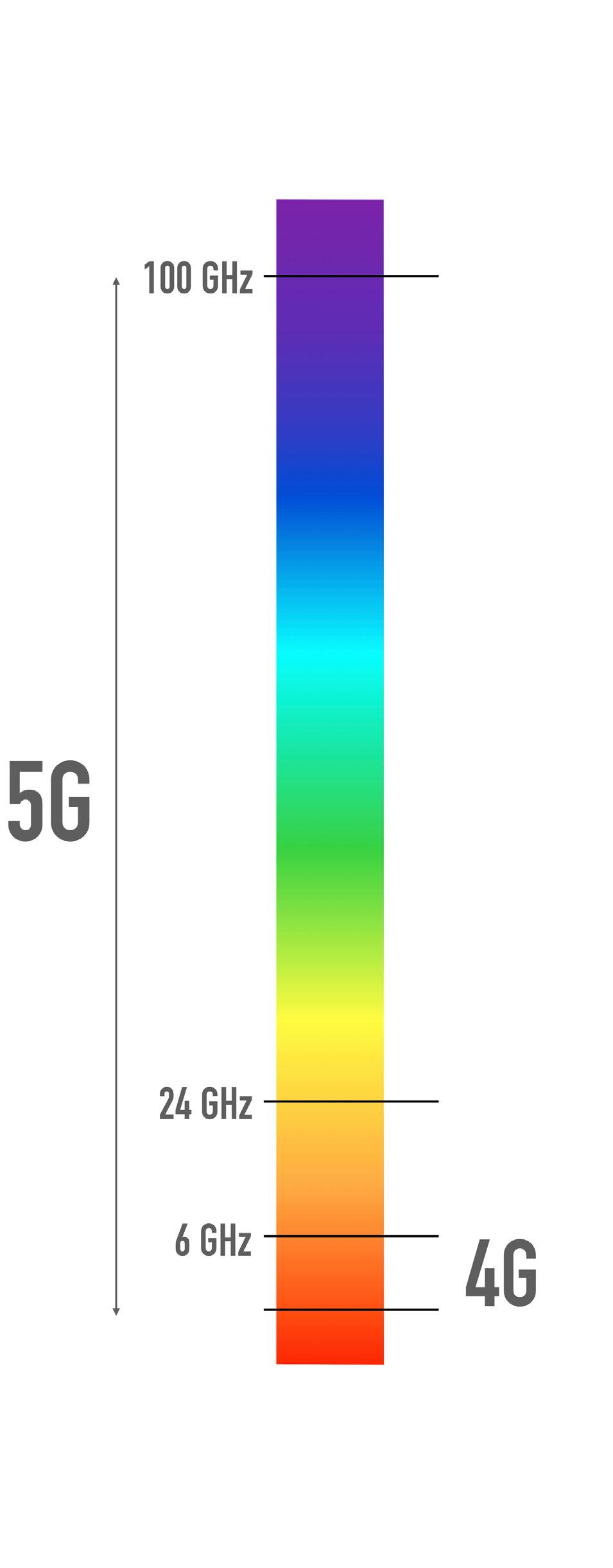
Large Millimeter Wave Bandwidth Opportunity, Adobe Stock.
37 DESIGN WORLD — EE NETWORK 05 • 2024 eeworldonline.com | designworldonline.com 5G SERVICES
Ad Index
SALES
Jami Brownlee jbrownlee@wtwhmedia.com 224.760.1055
Jim Dempsey jdempsey@wtwhmedia.com 216.387.1916
Mike Francesconi mfrancesconi@wtwhmedia.com 630.488.9029
Courtney Nagle cseel@wtwhmedia.com 440.523.1685
LEADERSHIP TEAM
CEO
Scott McCafferty
smccafferty@wtwhmedia.com
Jim Powers jpowers@wtwhmedia.com 312.925.7793 CFO
310.279.3844
EVP
Marshall Matheson mmatheson@wtwhmedia.com 805.895.3609
kgradman@wtwhmedia.com
773.680.5955
Digi-Key Electronics .............................................IFC Lemo USA 1 Coilcraft ................................................................... 4 NXP Semiconductors ............................................. 18 I-PEX,INC BC 5G, Wireless, & Wired Communications Handbook • May 2024
Ken Gradman
MHF® Micro RF Connectors
MHF® 7S
ZenShield® EMI shielding
Excellent VSWR performance:
1.5 max at 15 GHz
Locking Connectors:
MHF® I LK & MHF® 4L LK
Patented mechanical locking function for high-shock/vibration environments
Max. frequencies: 9 GHz, 12 GHz
MHF® 4L
M.2 industry standard
Max. frequency: 12 GHz