


Renesas offers a comprehensive portfolio of power management ICs and module solutions across the widest range of power requirements, making us the premier power partner for your most challenging design needs.


• Trusted, highly reliable, best-in-class power solutions
• Reference designs and tools that accelerate time-to-market


• Solutions that seamlessly connect to our industry-leading MCUs and MPUs


renesas.com/power-management


05 Editorial Note
Cold starts, hot power markets, and great expectations
06 Increasing voltage demands unleash opportunities for silicon carbide
(SiC) devices
The trend towards higher voltages opens new opportunities for design with Silicon Carbide.
10 High-density power for the AI revolution
Safe, powerful, integrated GaN power holds key to efficiency and sustainability.
15 Delivering power supply reliability in mission-critical systems
There are several factors to consider when selecting a power supply that delivers the high voltages often needed by large and complex hiigh-performance systems.
20 How advanced control strategies and system architectures contribute to sustainability
Technological developments are fast-producing step function improvements in performance.
23 How to quantify pulse current capability of SiC FETs
Silicon Carbide FETs go beyond silicon to extend reach to high pulse currents in power conversion applications.
28 High-density power-conversion technology enablers using GaNA Sub-Tereraheertz 6G
Modern electronics necessitate compact, high-efficiency power suppliees that can economically convert AC grid power into a suitable form.

Today’s electronic engineers are challenged by multiple factors. Research over the years has illustrated common trends that you, as engineers, deal with including keeping your skills up-to-date, shrinking time-to-market windows, fewer engineers and smaller design teams for large projects and evolving technological trends. The bottom line is that you must continually update your engineering knowledge base to be successful in your work.
Throughout 2024, we are presenting a series of online educational days. Each webinar will address specific design challenges, new techniques, and engineering skills.
For more information and to register for these webinars, go to:
EETRAININGDAYS.COM

FEBRUARY 1ST
ADAS DOMAIN
CONTROLLERS AND TRANSITION TO CENTRAL COMPUTE
FEBRUARY 8TH AUTOMOTIVE
INTELLIGENT POWER DISTRIBUTION
FEBRUARY 15TH
CHOOSING THE IDEAL SEMICONDUCTOR
TECHNOLOGY FOR YOUR TOPOLOGY: EXAMINING TRADEOFFS IN SI, SIC, AND GAN
VP, Digital Marketing
Virginia Goulding vgoulding@wtwhmedia.com @wtwh_virginia
Digital Marketing Coordinator
Francesca Barrett fbarrett@wtwhmedia.com @Francesca_WTWH
Digital Design Manager
Samantha King sking@wtwhmedia.com
Marketing Graphic Designer
Hannah Bragg hbragg@wtwhmedia.com
Marketing Graphic Designer
Nicole Johnson njohnson@wtwhmedia.com
Webinar Manager
Matt Boblett mboblett@wtwhmedia.com
Webinar Coordinator
Halle Sibly hkirsh@wtwhmedia.com
ONLINE DEVELOPMENT & PRODUCTION
Web Development Manager
B. David Miyares dmiyares@wtwhmedia.com @wtwh_WebDave
Senior Digital Media Manager
Patrick Curran pcurran@wtwhmedia.com @wtwhseopatrick
PRODUCTION SERVICES
Customer Service Manager
Stephanie Hulett shulett@wtwhmedia.com
Customer Service Representative
Tracy Powers tpowers@wtwhmedia.com
Customer Service Representative
JoAnn Martin jmartin@wtwhmedia.com
Customer Service Representative
Renee Massey-Linston renee@wtwhmedia.com
Customer Service Representative
Trinidy Longgood tlonggood@wtwhmedia.com
FINANCE
Accounts Receivable Specialist
Jamila Milton jmilton@wtwhmedia.com


cold spells across the United States have shifted the focus from “range anxiety” in electric vehicles (EVs) to concerns about their performance in cold...how they start, and how far they can go. Buzzworthy? Apparently. Newsworthy? Maybe, but it's not new news.
Reflecting on a youthful personal experience with a three-on-the-column 1964 Dodge Dart, “range anxiety” meant the onerous mental calculations involved in determining how much spare change was needed to get enough gas to reach home after a night out. “Cold starts” involved the struggle of starting an internal combustion engine (ICE) in Northeastern Pennsylvania winters, usually resulting in a dead battery with whining, rapid clicking, and the anxiety of locating someone for a jump start.
The current discourse around EVs seems to reflect the unrealistic expectations of technology overall — almost understandable given the rapid advancements in electronics to which consumers have grown accustomed. The intricate electronics found in EVs and most of the electronic devices we use daily didn’t simply materialize out of thin air. Developing these power electronics devices is a complex process, and the engineers who bring them to life are highly skilled professionals.
Contributing writer Bill Schweber, in a recent EEWorld Online blog post, emphasized the underappreciated role of engineers in these technological advancements who are frequently overshadowed by the pop culture that benefits most from their engineering advancements:
“My view is that non-recognition is the downside of innovating so much while making it all look so easy, regardless of how hard it was. In many ways, the astounding success of the engineering community at creating so much wonderful stuff, with the resulting advances we live with and routinely use, makes it all look like no big deal: it all “just happens.” Of course, it’s not that way at all.”
As consumers, we often take for granted the complex technology and sophisticated engineering skillsets that power our everyday lives. We expect constant connectivity, rapid charging, and minimal latency when browsing, streaming, or listening online. Similarly, do we think our EV batteries should be unaffected by cold weather, and the driving range on a
single charge be comparable to that of a full gas tank?
The transition to electrification, the rise in the number of power electronic components in EVs, and the integration of artificial intelligence into numerous applications are just some of the challenges electronics engineers face today. The solution to these challenges will involve the efficient use of currently available power and significant leaps in energy generation for the power-intensive needs of the future.
It’s not simple stuff, but reigning in expectations appears a lot more complicated. Demand does help to inspire and drive innovation. Maybe it’s time for demanding consumers to spend more time in the driver’s seat with the folks behind that innovation.
The articles included here are definitely for you, the engineer. But it wouldn’t hurt to pay it forward to those who benefit from your work. They don’t have to know what RDson or bidirectional power means in detail; maybe it would be more impactful to explain what you do in a context they can appreciate — and not take for granted.


The trend towards higher voltages opens new opportunities for design with Silicon Carbide.
Didier Balocco, EMEA Power Solutions Group Business Marketing Engineer, Power Solutions Group, onsemiWITHits higher electron mobility, lower losses, and ability to work at higher temperatures, the case for silicon carbide (SiC) devices in challenging power applications is widely accepted. While the benefits of silicon are significant in key applications, further advancement is required, especially to reduce size and cost while improving efficiency.
In the automotive and renewable sectors, there is a trend towards increasing voltages to meet these goals. SiC devices capable of operating at these voltages must be freely available to achieve this.
The move to higher voltages to increase efficiency has its foundations in the most fundamental law in physics, Ohm's Law. This tells us that losses increase with the square of current; therefore, reducing current significantly improves efficiency. Ohm's Law also tells us that, for the same power, we have to double the voltage if we want to halve current.
In halving the current, the static losses due to conduction losses in semiconductors and cabling are reduced by a factor of four. It is for this exact reason that electricity
grids operate at extremely high voltage levels.
While it might seem evident that industrial and automotive applications move to extremely high voltages, this is impractical due to the availability of components supporting such voltages.
In a switching power converter, a power device has three roles: blocking, conducting, and switching between the
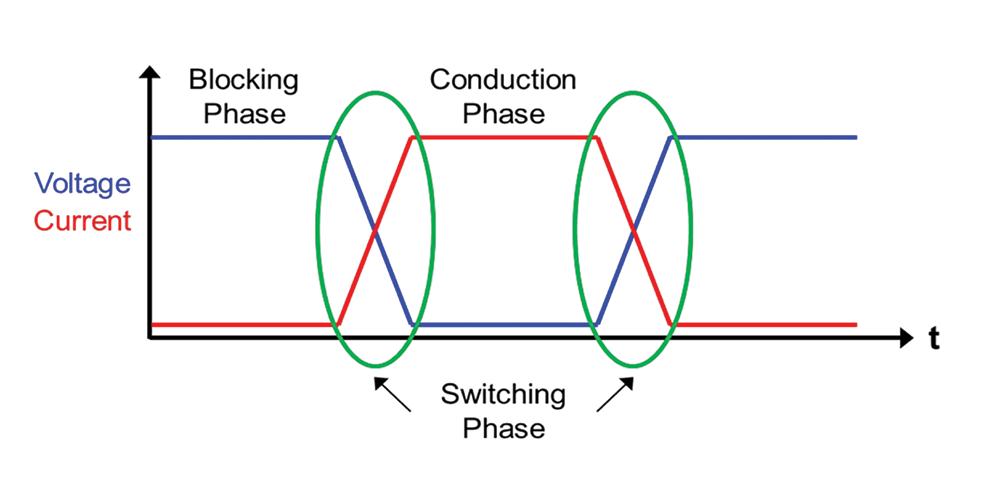
previous roles. As voltage increases, the challenge is with the blocking aspect, as high voltages will appear across the device, and without the appropriate construction and materials, a catastrophic failure could occur.
Therefore, SiC devices with higher blocking voltages across their drain and source pins (VDS) will be required to access the efficiency benefits of a higher voltage operation. Currently, many devices with 650 V capability and 1200 V-rated devices are becoming more common. However, higher voltage-rated devices will be required to address these higher voltages, with an appropriate design margin to ensure reliability.
Applications operating at higher power levels will benefit significantly from greater efficiency. In the renewable field, both wind and solar power generation are moving to higher voltages. With solar photovoltaic (PV) systems, the DC bus voltage from the PV panels has increased from 600 V to 1500 V to enhance efficiency.
Greater efficiency here simply means that more natural solar or wind energy is available to be used immediately or stored for later use. While both forms of energy may appear to have infinite capacity, they are both subject to the vagaries of weather, which can limit output.
Also, if the system is more efficient, it will be smaller and lighter, which is a significant benefit for roof-mounted installations.
One of the reasons often cited for
slower-than-expected growth in EVs is the time taken to charge and the limited battery range. To address this, automakers are replacing 400 V battery strings with 800 V versions. Charging speed is determined by the charger's output power, which is limited by the system voltage and output current. While increasing the current reduces charging times, it also increases the heat generated and system energy loss, reducing the charger's efficiency and elevating the cooling demands. Alternatively, the EV charger's power output is significantly increased by increasing the voltage and maintaining a similar current level. This lowers the vehicle's charging time without substantially raising the thermal considerations or reducing system efficiency.
The reduced current and enhanced efficiency will reduce the on-board charger's size, cost, and weight (OBC) as thinner cables can be used and less heatsinking is required. As the OBC remains on the vehicle, any weight reduction will increase the vehicle's range.
Looking to the future, as electric propulsion moves into commercial vehicles, the batteries will be significantly larger, and more power will need to be transferred efficiently to charge in a reasonable time. As a guide, the Megawatt Charging System (MCS) is rated for a charge rate of 3.75MW – 3,000A @ 1,250 VDC.
One of the challenges in developing semiconductor power devices in vertical
structures with higher breakdown voltages is that there is a corresponding increase in conduction losses due to the increase in RDS(ON). The drift layer is generally thicker in devices with higher withstand voltages, which increases conduction losses.
So, while there are efficiency benefits to increasing operating voltage, the corresponding increase in conduction losses within the MOSFET will negate some or all of these benefits.
SiC-based power devices can offer higher breakdown voltages with a substantially thinner drift layer than the equivalent silicon device, resulting in lower forward voltage drop and reduced conduction losses.

With the need for MOSFET devices with breakdown voltages in excess of the operating voltage, onsemi has developed a range of SiC MOSFETs specifically for such applications.
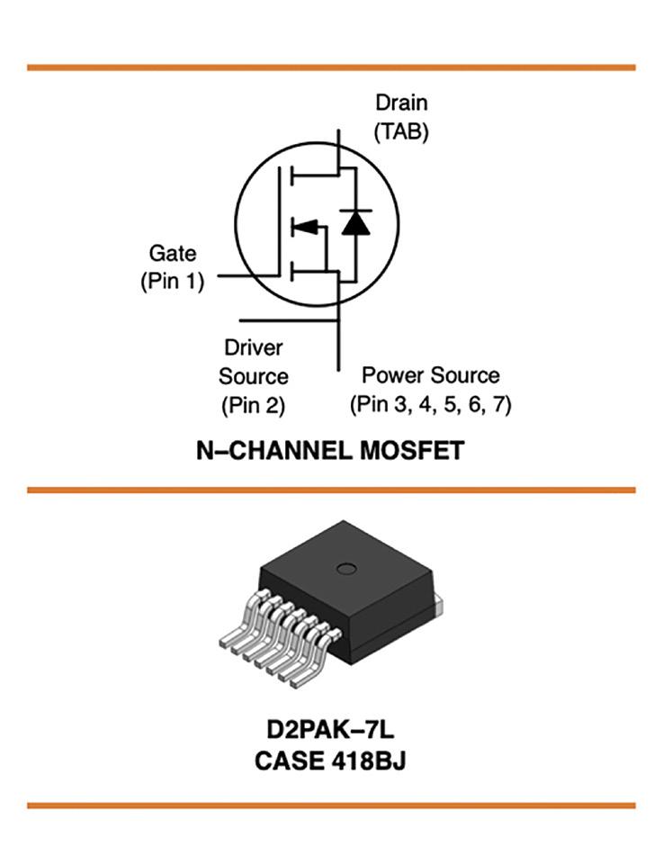
onsemi's NTBG028N170M1 is an N-channel planar EliteSiC MOSFET that is optimized for fast switching applications at high voltages with a VDSS of 1700 V and an extended VGS of -15/+25 V. The device can support drain currents (ID) up to 71 A continuously and 195 A when pulsed.
The robust device mitigates conduction losses with an excellent RDS(ON) value of just 28 mΩ (typ.), while an ultra-low gate charge (QG(tot)) of just 222 nC ensures low losses during high-frequency operation. The device is housed in a surface mountable D2PAK–7L package, which reduces parasitic effects during operation.
Supporting the MOSFETs, onsemi offers a range of 1700 V-rated SiC Schottky diodes that enhance the voltage margin between VRRM and the peak repetitive reverse voltage of the diode. In challenging applications, the 1700 V diodes will deliver lower VFM, maximum breakdown voltage, and excellent reverse leakage current even at high temperatures, thereby equipping design engineers to achieve stable high voltage operation at elevated temperatures.
In every area of power electronics, efficiency is a primary goal. Not only does it reduce operating costs, but it also allows designs to be smaller, lighter and lower cost. With highly efficient semiconductors already commonplace, designers are looking to other areas of the system to deliver more efficiency. Increasing the system voltage reduces the current and has a significant impact on reducing losses. However, this has proved challenging until now, as increasing the breakdown voltage of MOSFETs has also increased their conduction losses.


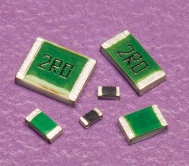
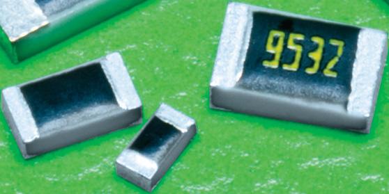


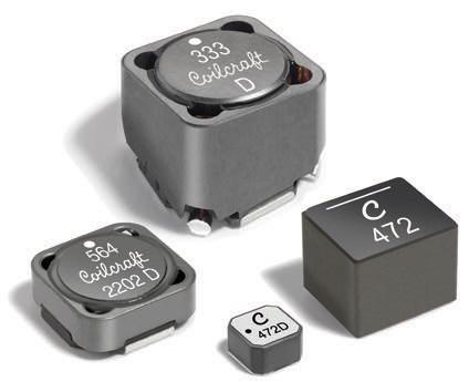
Coilcraft voltage-rated inductors support applications such as high-voltage DC-DC and AC-DC power supplies, industrial and home automation controls, appliances, and automotive, including electric vehicles (EVs).
Our XEL and XGL Families of molded power inductors offer operating voltage ratings from 60 V to 120 V, and many of our
Coilcraft offers a wide range of voltage-rated power inductors that assure the safe, reliable operation of your designs. WWW.COILCRAFT.COM
LPS and MSS Family inductors are suitable for 400-volt operation or higher.
Our new MSS1514V Series offers an 800 V rating in a 15.5 x 15.5 mm footprint, with excellent current handling and low DCR.
Learn more about operating voltage ratings for inductors and see our full line-up at www.coilcraft.com/ HighVoltage.
®

Safe, powerful, integrated GaN power holds key to efficiency and sustainability.Charles Bailley, Senior Director Global Business Development, Navitas Semiconductor
it burst into the mainstream with the public availability of ChatGPT and Google Bard, Artificial Intelligence (AI) has dominated the technology news landscape. Indeed, such is the level of buzz around AI, even the least technical consumer understands what it is and how it might benefit or impact them.
AI in the industrial and consumer spaces is dominated by powerful, purpose-designed processors from large, established companies like Nvidia and start-ups and scale-ups who are helping to fuel innovation. These increasingly powerful ‘superchip’ platforms are essential for processing huge volumes of data at speeds that enable AI to fulfill its potential. But implementing these technologies presents challenges. As AI proliferates, the extreme power demanded by processors such as NVIDIA’s Grace
Hopper H100 super-chip require a two- or three-fold increase - from around 30 to 40 kW per cabinet in current servers to 100 kW or more.
There are physical considerations too. The space afforded to power, processing, and server systems cannot
expand without limit, making power density a priority for system architects.
The carbon footprint of data centers is already significant thanks to the amount of energy needed to power and cool servers that provide the cloud-based services we rely on. The International Energy Agency (IEA) estimates global data center electricity consumption in 2022 at 240-340 TWh, or between one and 1.3% of total global electricity demand. The growth of AI and the increasing amount of data being generated, shared, and stored by everything from smartphone apps to connected vehicles will further increase this demand. A spotlight has been thrown on the sector to do more to minimize energy use and maximize efficiency.
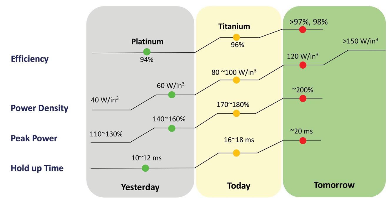
While operating expense pressures mean there is a natural desire in industry to improve matters, power supply performance and efficiency targets are also driven by regulations, standards and frameworks. For example, the latest European regulations expect server power
supplies to exceed the 80 PLUS Titanium efficiency specification. Certification to this most demanding of the 80 PLUS family of regulations requires guaranteed power supply efficiency between 90% and 96% at loadings from 10% to 100%. Compliance also requires a power factor of at least 0.95 at lower levels — a benchmark that necessitates active power-factor correction.
With so many server farms installed worldwide, physical server rack-size constraints are well-established and hard to change. As a result, the processing power needs of AI now and in the future must be implemented within existing space constraints, with thermal management arrangements compatible to the cooling requirements of legacy (lower) power densities. This means the greater processing and power densities associated with running AI chips must be achieved without creating heat that may be hard to manage without additional, power-hungry colling technologies.
The tough demands of the enterprise
and hyperscale markets have driven the formation of the Open Compute Project. This respected community (including big names like Facebook, Intel, Google, Microsoft, and Dell) seeks to define the common redundant power supply (CRPS) specification to ensure modularity for easy replacement and maintenance, and flexibility to address different and emerging applications for IT ecosystems. As well as redundancy, CRPS mandates that rack power must continue to be provided in a 1U (40 mm) x 73.5 x 185 mm form factor.
With server power demand set to increase towards 100 kW, pressure to meet 80 PLUS Titanium specifications and requirements to comply with the OCPdefined CRPS specification, the challenge for power designers is significant. A closer look at a typical compliant power supply provides some insights into the technology evolution that is needed.
The most commonly used topology for data center server power supplies employs silicon MOSFETs and has a boost power factor correction (PFC) stage followed by an LLC resonant converter.
Increasing power demands associated with AI workloads requires multiple outputs when using LLC transformers to minimize conduction losses of secondary windings and synchronous rectifiers (SRs). Combining windings and SRs in parallel can achieve lower winding resistance but the more pronounced termination losses this causes (as switching frequency increases) negatively impacts overall system efficiency.
Using multiple transformers in parallel instead of windings and SRs can help by lowering AC-related conduction losses and leakage flux resulting in reduced leakage inductance. This approach can also simplify terminal design. The flipside is that multiple transformers introduce larger core losses and a larger magnetic size. Deploying matrix transformers can be a way to mitigate these losses, but using traditional wire-based transformers in any form means the physical size of the converter becomes an issue in an operating environment where power is increasing but space is not.
PCB-based planar transformers can provide a space-saving and cost-effective answer to the challenges described, but due to the limitation on the number of PCB
windings possible within the circuit board structure, they can only be used when the switching frequency is high enough to support a minimum number of turns.
A fundamental issue is that silicon has reached its performance limits in terms of suitability for many new and emerging applications. In high-density CRPS applications, swapping out silicon MOSFETs with GaN devices allows much higher switching frequencies and supports the use of planar transformers. GaN technology also helps designers to keep switching losses within the scope of 80 PLUS Titanium specifications, as well as supporting improved robustness, higher power densities.
However, it is important to choose the right type of GaN device. Discrete GaN FETs, for example, have a relatively fragile gate. A much better — and simpler — alternative can be realized by selecting integrated GaN devices.
Monolithically-integrating a GaN gate driver circuitry on the same chip as the GaN FET avoids the issues of using discrete GaN
devices, helping designers properly control gate voltage as well as keeping component count down. But the latest integration levels go far beyond that to incorporate control, sensing, and protection. These next-generation integrated GaN platforms are setting new industry benchmarks in efficiency, density, and reliability for demanding applications.
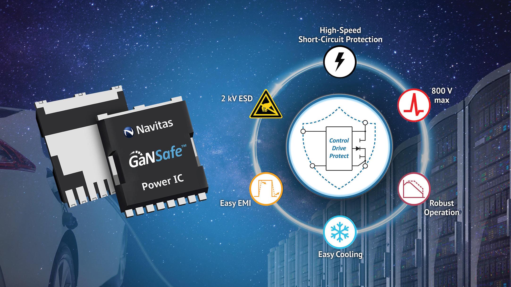
Take, for example, the Navitas GaNSafe™ family.
Conceived specifically to meet the needs of AI-based data centers and other high-power, fast growth applications such as EVs, solar and battery energy storage systems (BES), GaNSafe provides the switching speed, efficiency, and power density that addresses the challenges of, 80 PLUS Titanium and IT ecosystem defined by the OCP. Supplied in cool-running, surfacemount TOLL packages, these ICs have inbuilt algorithms for dead-time control and a suite of additional safety features needed for high-power applications.
Certainly, it’s hard to overstate the importance of protection, safety and robustness for devices deployed in data center servers, where issues associated
in comparison to existing 3,200 W CRPS solution.
with device, module, or system failure can be costly or even dangerous, with a major impact on the infrastructure they support. That’s why GaNSafe has highspeed protection built-in, including with autonomous ‘detect and protect’ that acts within 50 ns. ESD protection — not normally part of the specification of discrete GaN transistors — is also included to protect against events up to 2 kV. Further protection against extraordinary application conditions comes from a 650 V continuous and 800 V transient voltage rating. In addition, programmable turnon and turn-off speeds ease the job for designers trying to meet EMI regulatory requirements.
GaN in action — application example
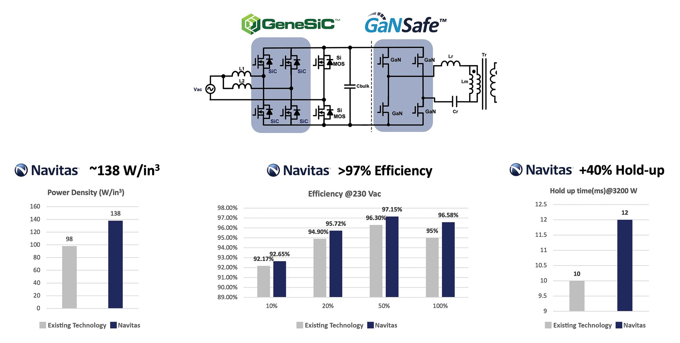
An AI data center server power supply built using devices such as GaNSafe can


achieve significantly better performance and support enhanced system safety and reliability, versus a unit that utilizes discrete silicon or silicon carbide (SiC) devices.
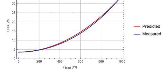
To demonstrate potential performance improvements, Navitas has created a reference design for a 54 V AC-DC data center AI/GPU server power supply in a CRPS185 format using Navitas’ GaNSafe and GeneSiC technologies. This design demonstrates that power density can be increased from less than 100 W/ in3 to 138 W/in3, which translates to a power output improvement from 3.2 kW to 4.5 kW (Figure 3).
In addition to improved power, efficiency improves to over 97%, reducing waste power and mitigating the need for additional thermal management provision. Hold-up time goes up by around 40%, contributing to reduced risk of data loss

or hardware damage in the event of power interruptions.
Delivering the increased processing and capacity demanded by mainstream AI and machine learning (ML) applications requires new approaches to power delivery and management to ensure performance while addressing design, commercial and legislative requirements related to size, efficiency, and sustainability. Implementing these new approaches means moving away from conventional silicon and discrete GaN semiconductors to GaN devices that feature high levels of integration. By choosing ICs that combine control, switching, sensing, and protection into a single device — for example, it is possible to develop highly efficient power supplies with significantly higher power ratings within existing form factors.


There are several factors to consider when selecting a power supply that delivers the high voltages often needed by large and complex highperformance systems.
John Toro, Customer Solutions Engineer, Advanced Energy
FORalmost all electronic products and systems, high reliability should be expected. Reliability should not be compromised or a trade-off for other performance factors. In particular, missioncritical industrial and medical applications, which require almost constant use, are expected to provide reliable operation over many years. So, a fundamental design requirement is choosing underlying subsystems and modules that can deliver on this expectation.
In terms of overall reliability, power supplies are especially important. A failure of these critical assemblies means a complete system failure and downtime that, at best, can impact cost and, at worst, could be the difference between life and death.
A wide range of high-voltage DCDC power supplies are available including products that are optimized for industrial and medical applications.
In this article, we will look at some key factors to help ensure optimized reliability when choosing and designing-in precision DC-DC high-voltage power supplies.

In today’s competitive markets, reliability is vital. The cost of unexpected failure can be exceptionally high in specific missioncritical applications. Many applications that require high-voltage power fall into the “mission-critical” category. In the world of semiconductor manufacturers, for example, failure of a high-voltage power system used for plasma generation would be expensive in terms of system downtime and the need to scrap work in progress. The same is true in other industrial applications ranging from factory automation to glass manufacture. In the medical field, where high-voltage supplies have become a fundamental element of equipment used for monitoring, diagnosis, and treatment, the consequences of failure can range from misdiagnosis to serious patient harm.
With the wide range of potential applications for high-voltage power supplies, it is no surprise that many types are available. These include everything from large multi-kilowatt rack-mount
designs to lower power solutions with output voltages in the tens of kilovolts. In addition, there are smaller, modular supplies as well as PCB-mount DC-DC converters for delivering high voltage to the point of use.
While specifications are essential in selecting an appropriate solution for a given application, it is only part of the story. Equally important when considering reliability is an understanding of the design process behind the power supply and the margins employed during that process.
Six of the most important areas to consider are:
1. Ideal operating range
Ensuring a power supply is used within its ideal operating range is important to maintain long life and reliability. Some suppliers will place restrictive caveats on these operational windows, while
others design their solutions to operate indefinitely at their maximum voltage and current ratings. Achieving this requires careful planning of design margins.
For example, critical components in the high-voltage section (such as capacitors, diodes, and magnetics) must be selected with ample voltage margin. Also, the geometry of traces on circuit boards must be able to carry more than the required current levels while keeping metal content to a minimum. Components with elevated levels of thermal dissipation need to be kept far away from temperature-sensitive components to reduce internal heating effects, which can affect temperature coefficient, stability, and overall product reliability.
Modern, compact, high-voltage DCDC power supplies use some form of encapsulation to increase power supply reliability. Simply relying upon the physical spacing of high-voltage components in an open-air design drives up the size of the
product to unmanageable scale. Over time, creepage paths will become compromised due to the inevitable ingress of dust, contaminants, and moisture.
Therefore, selecting the right encapsulant is critical and challenging. Suitable materials exhibit extremely high dielectric strength, but physical properties are also essential. Designers must choose materials with the highest combination of thermal conductivity and dielectric strength for their products. This ensures that these products will last through extended voltage breakdown resistance and long-term resistance to thermal degradation.
3. Power dissipation
The power dissipation of a typical highvoltage DC-DC supply is closely related to its power density. A supply designed to be as compact as possible, using the best creepage path and encapsulation design principles, will have a small volume, which can be desirable in space-constrained applications. This can complicate thermal dissipation because there is less available surface area from which to extract heat.
Additionally, care must be taken to ensure that components that dissipate relatively elevated heat levels (such as MOSFETs and driver amps) are physically located as close as possible to thermally conductive planes to allow heat to escape. This must be considered during the initial design phase of all products, including volume, footprint, and location of thermally active components. Achieving the ideal balance of size and thermal characteristics gives the user the smallest volume possible while ensuring long-term reliability.
4. Electrical connections
Using connectors and conductors that are properly sized for the applied voltage and the current level they must carry will also increase product lifespan and reliability. For low-voltage conductors, a comfortable margin is applied during the selection process to keep contact resistance to a minimum. This translates into less heat dissipation, which delivers higher reliability.
Conversely, if superior design principles are not applied, high-voltage output cables and connectors will be subjected to punishing attacks from
ionization. The effects of ionization can become a serious reliability factor within the power supply. The most common contributors are sharp points and edges of trimmed component leads and poorly designed printed circuit board (PCB) circuit traces, which create high-voltage gradients. Over time, these gradients will break down the dielectric properties of even the best encapsulation compounds, cause “tracking” (PCB surface arcing), and lead to irreversible failure of the power supply. Techniques such as “ball soldering” can be applied to prevent these potential failures during the construction of the high-voltage sections. Unique to the high-voltage power supply industry, ball soldering increases reliability by eliminating sharp points and narrow edges on the PCB.
Robust product development based on time-proven construction techniques and the careful selection of high-voltage cables and interconnections will ensure long-term reliability by eliminating ionization-induced degradation.
5. Arc & short circuit protection
It is important to consider that arcing may occur outside the power supply – an unpleasant facet in nearly all high-voltage applications. With that in mind, designing a power supply to withstand arc occurrences is integral to the design cycle. This often means strategically placing arc-clamping components at all key connections, including but not limited to the DC input, I/O, and high-voltage return paths. After installation, these safeguards must be exhaustively evaluated by simulating arcing conditions at all expected intensity and frequency levels. This makes for a robust, reliable package that can be deployed in even the most demanding applications.
6. Design verification
After the initial design phases, products need thorough design verification testing. This step verifies that all the above design considerations will contribute to optimized reliability in the field. Once the power supply has passed this development phase,
it is considered ready for manufacture.
Choosing a well-designed and optimized power supply helps mitigate potential reliability issues in the field. Additionally, choosing the right power supplies can contribute to overall system reliability, as power supplies can help monitor overall system health and predict and prevent failures.
Abrupt failures rarely happen without any degradation or warning, provided you know where to look or listen. For example, a worn bearing in a fan or other mechanism will produce louder audible noise and may have more resistance to turning, which will increase motor current. A failing capacitor may lead to more ripple and noise on the supply line.
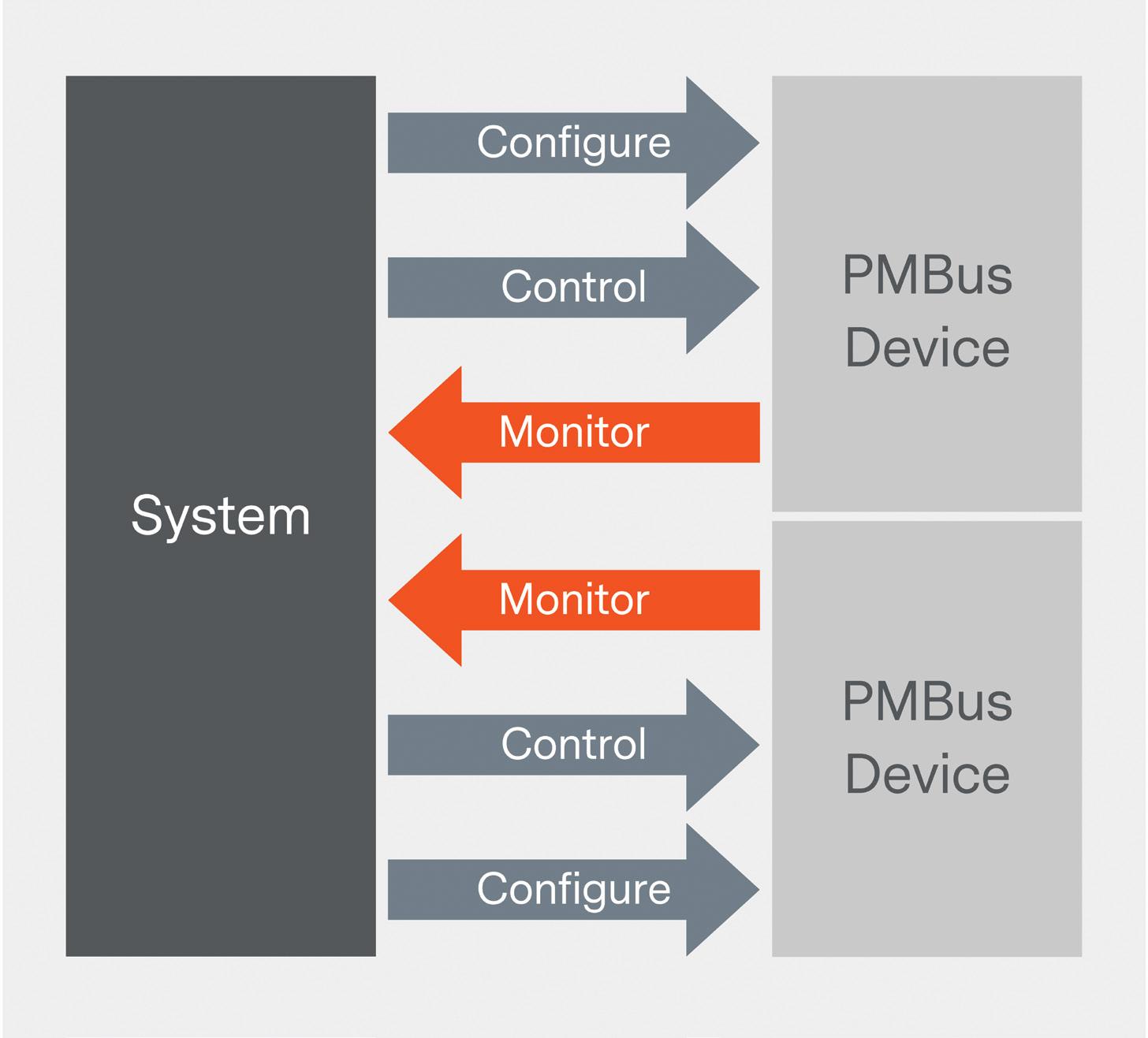
Monitoring the power supply can detect these types of fault trends before failure or out-of-specification operation happens. One of the most significant advances in power supply intelligence is the Power Management Bus — or PMBus.
This standard provides a means of controlling and monitoring a power supply through digital communications. Electrically compatible with an InterIntegrated Circuit, or I2Cv (while offering more features and overcoming noise-related and other issues sometimes associated with the latter), PMBus, in conjunction with suitable software, allows for monitoring of the telltale signs of change that often occur before a failure. As a result, preventative maintenance can be implemented to minimize or eliminate potential system downtime.
High-voltage power is essential to many mission-critical systems where the consequences of failure are high. Selecting a suitable unit with sufficient margin for the application is a good starting point to reduce the risk of failure. Furthermore, understanding the design process in critical areas can
also ensure longevity. Intelligent power supplies incorporating technologies such as PMBus can support monitoring that provides insight into key aspects of the wider system, providing advance warning of degradation / impending failure and allowing for low-cost preventative maintenance.

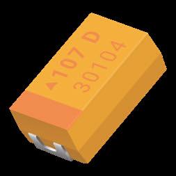
Tantalum Capacitor
•Audio Systems
•GPS
•Seat Controls
•Dashboard
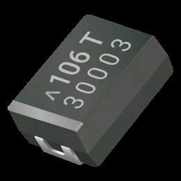
Polymer Capacitor
•Body Electronics
•Cabin Controls
•Infotainment
•Comfort

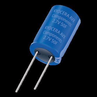
SuperCapacitor
•eLatch
•eCall
•Motor Stabilization
•eVideo / eCamera


Technological developments are fast-producing step function improvements in performance.
Jeff Shepard
something the same way as in the past rarely produces improved results. Technology constantly evolves and improves, and new technologies can require new approaches. In the case of the power electronic systems discussed below, artificial intelligence (AI) and machine learning (ML) are common themes in these advanced control strategies and system architectures. Another development is using the Internet to offload computationally intense activities like ML functions to reduce system costs. All these developments lead to performance and efficiency improvements and contribute to sustainability.
This article begins with a look at multiplexing uninterruptible power supplies (UPS), considers the benefits of using deep reinforcement learning (DRL) with distributed renewable energy generation, reviews several control strategies for voltage source converters (VSCs) in distributed generation (DG) and microgrid systems and closes by presenting the possibility of using distributed power factor correction (PFC).
Power converter efficiency is affected by the loading factor. Light loading generally leads to lower efficiency. Loading conditions can vary widely in applications like UPSs in a data center. In addition, there’s a desire for
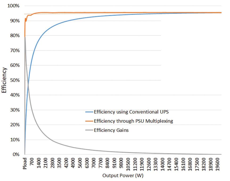
redundant operation. Various redundant configurations have different loading factors. For N+N redundancy, the loading factor is about 50% or lower. For N+1 redundancy, the loading factor can be higher but variable in most installations.
To address the challenges of variable UPS loading, power supply unit multiplexing (PSUM) has been designed to improve loading factors and control redundancy levels like N+0, N+1, or N+N. While developed specifically for use with UPSs, the same concept is expected to be usable in any power conversion system with variable loading, including industrial installations and electric vehicle infrastructure.
Of course, loading is only one factor. Input voltages and other factors can also affect efficiency. And different UPS implementations can offer different efficiencies. In a system consisting of several UPSs that vary in size and other factors, the PSUM is designed to turn on and off various combinations of UPSs to achieve optimal efficiency based on realtime loading conditions and to support the required level of redundancy, which can also be a variable in the system. The control is based on the measured efficiency values for the individual UPSs combined with machine learning to identify the optimal combination of UPSs for maximum efficiency and the required redundancy (Figure 1).
Power grid operators are being challenged by the increasing use of distributed renewable energy generation from wind farms and photovoltaic installations that
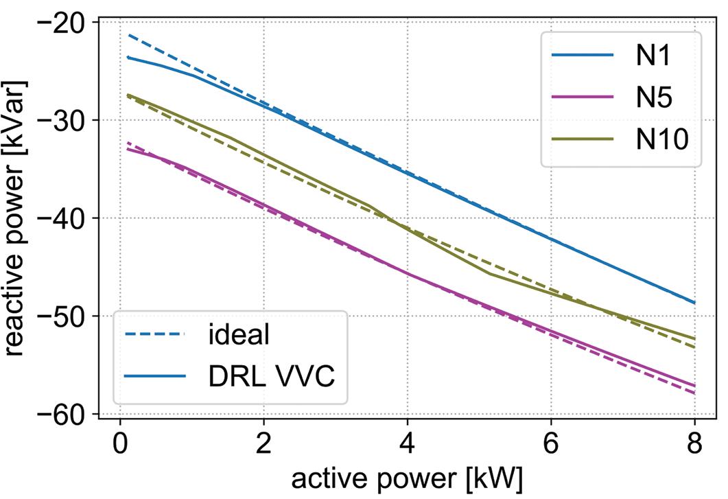
can result in significant fluctuations in the grid voltage. Those fluctuations are often dealt with using reactive power — volt-amperes reactive (var) — to ensure grid integrity. However, using a centralized control process to arrive at the correct volt-var balance in real time and effectively deal with distributed renewable generation sources is difficult. Deep reinforcement learning (DRL) may provide a solution.
DRL is already being used in robotics and other applications. It’s being applied to power grids to control the operation of dispersed and networked voltage regulation devices. DRL algorithms combined with a deep deterministic policy gradient (DDPG) agent are being explored using smart inverters in volt-var control (VVC). DDPG is a reinforcement learning agent that searches for an optimal policy that maximizes the expected cumulative long-term reward.
The test simulation included a variable PV energy source. The control algorithm continually adapts to short-term fluctuations in power flow and to changing grid connections over the long term without needing any network connection. The system required real-time independent control of reactive power from -20 to -60 kvar at several power nodes to maintain a level grid voltage (Figure 2). For purposes
of the study, a tight voltage tolerance was imposed. A wider voltage tolerance can be used in a real-world grid, meaning less reactive power would be needed, making it easier to implement DRL VVC.
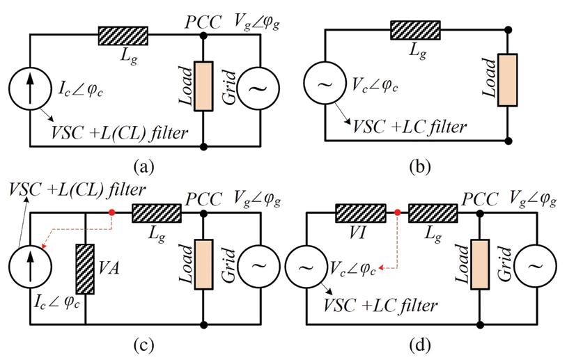
VSCs are used in EVs, microgrids, and similar applications. VSCs are used for three primary purposes in distributed generation and microgrids: grid forming, grid feeding, and grid supporting (Figure 3). Grid-forming inverters use a rigid voltage control, grid-feeding inverters use a rigid current or power control, and grid-supporting inverters use a flexible combination of voltage, current, and/or power control depending on microgrid conditions. In addition, grid-forming inverters define the grid and, therefore, don’t require grid synchronization, while grid-supporting and grid-feeding inverters require synchronization.
Control schemes for VSCs in DG systems and microgrids are divided into inner and outer control loops. Inner loops control the operation in the VSC, while outer control loops control the interaction of the VSC with the grid. Advanced control schemes can be further divided into model- and data-based techniques. Model-based control techniques use a mathematical model of the VSC to derive the control signal. Examples of advanced model-based control include:
State Feedback Control (SFC) focuses on designing multiple input, multiple output (MIMO) control structures using multi-variable state-feedback controllers to
achieve predefined performance measures and is implemented using a modulator structure.
Sliding Mode Control (SMC) uses sliding surface functions based on linear combinations of various signals like the current error and its derivative, the output capacitor filter voltage error and its derivative, and derivatives and integrals of estimated currents and voltages. SMC uses a discontinuous feedback control that forces the system to equilibrium quickly based on a MIMO control structure.
Model Predictive Control (MPC) is an optimization strategy based on a predictive control model, a cost function, and an optimization algorithm. The cost function compares predicted state variables with reference values. MPC also allows the definition of a MIMO control structure to merge multiple control loops in a single stage. However, the lack of applicable stability analysis methods has limited the use of MPC.
Data-based control describes the controlled system using the available input/ output data. Data can be derived from a real system or a model.
Artificial Neural Network (ANN) control implements non-parametric function approximations using basic algebraic operations. ANNs can be trained to estimate any given nonlinear relationship between input and output data with a desired level of precision. They can be implemented as a direct or indirect control. ANNs can replace individual linear controllers in a cascaded structure or be implemented as a MIMO controller. ANNs can be used to implement finite control set (FCS) MPC control with very light computational needs (Figure 4). However, they suffer from practical drawbacks like
regular MCP implementations.
Fuzzy control uses function approximation rules to transform sets of inputs, like the error between a reference value and measured signal, into one or more control outputs or feedback signals. Fuzzy controllers have been developed to replace the current controller in a gird feeding VSC. They can also be used to implement a MIMO control structure.
PFC is generally implemented as a centralized function within a power converter or on a utility grid. A new approach to PFC has been developed based on remote configuration supported by real-time telemetry. This technique provides enhanced flexibility and adaptability and can change grid-connected capacitance values in real time as required to maintain the needed power factor.
While it can be important to provide real-time PFC support, it’s not usually a critical function demanding fast control loops. That means that the control algorithm can be remotely located and connected to the PFC equipment through the Internet, reducing the requirements for local computing power. This approach lends itself to using a real-time feedback loop and AI to improve PFC system performance continuously.
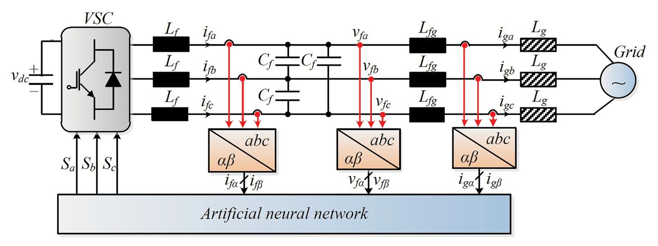
Figure 3. Basic structures of VSCs include (a) Grid-feeding, (b) Grid-forming, (c) Grid-supporting with current control, and (d) Gridsupporting with voltage control (Image: IEEE Transactions on Power Electronics).
Advanced control techniques are being developed for various power conversion, green energy, and power quality applications. In several cases, AI and ML are being used to improve performance, and the Internet is being used to offload computational complex operations, enhancing system flexibility while also reducing system complexity and cost.
A Novel Machine Learning-Based LoadAdaptive Power Supply System for Improved Energy Efficiency in Datacenters, IEEE Access
Adaptive Online-Learning Volt-Var Control for Smart Inverters Using Deep Reinforcement Learning, MDPI energies
Advanced Control Methods for Power Converters in DG Systems and Microgrids, IEEE Transactions on Industrial Electronics
Artificial Neural Network-Based Adaptive Voltage Regulation in Distribution Systems using Data-Driven Stochastic Optimization, IEEE
Improving the Efficiency and Sustainability of Power Systems Using Distributed Power Factor Correction Methods, MDPI sustainability.
Figure 4. ANNs have light computational needs and can be used to implement FCS MPC control in VSCs (Image: IEEE Transactions on Industrial Electronics).

Silicon Carbide FETs go beyond silicon to extend reach to high pulse currents in power conversion applications.
Pete Losee, Engineering Director, Power Devices, Qorvoband-gap (WBG) semiconductor devices, such as Silicon Carbide (SiC) field-effect transistors (FETs), are renowned for their minimal static and dynamic losses. Beyond these attributes, this technology can endure high pulse currents, proving particularly advantageous in applications like solid-state circuit breakers. This article delves into the characteristics of SiC FETs, offering a comparative analysis against traditional silicon solutions.
The ongoing pursuit to minimize power losses in semiconductor switches is spearheaded by WBG devices, with SiC FETs taking center stage. These devices, constructed as cascodes of a SiC junction-gate field-effect transistor (JFET) and co-packaged silicon metaloxide-semiconductor field-effect transistor (MOSFET), stand out as normally-off devices with user-friendly gate drives. Their impressive portfolio of “figures of merit” outshines competing technologies, specifically focusing on on-resistance per unit die area (RDSxA) — a metric capturing the combination of low static and dynamic power losses with cost-effectiveness. Despite their smaller die size which translates to more units per wafer and reduced device capacitances — SiC FETs defy expectations by exhibiting enhanced temperature tolerance and increased peak current capability. Let’s take a look at the numbers.
Quantifying the performance of a SiC FET,
exemplified by the 750V-rated device from Qorvo (part UJ4SC075005L8S in a TOLL package), reveals an RDSxA figure 2.2 times better than Gen 4 SiC MOSFETs, consistently maintained across the entire temperature range. In practical terms, this device displays an on-resistance of 5.4 mΩ at 25 °C and 9.2 mΩ at 125 °C, surpassing silicon or SiC-MOSFETs and Gallium Nitride high-electron-mobility transistor (GaN HEMT) rated at 600/650 V in the same package by a factor of 4 to 10.
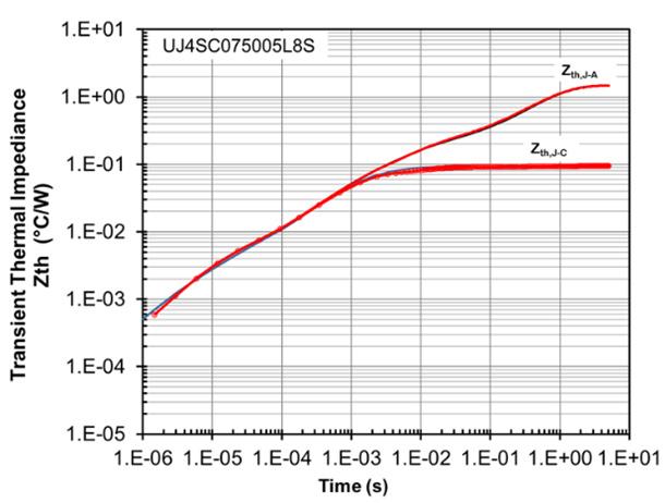
To leverage this ultra-low resistance for a high current rating, the sample SiC FET uses silver sinter die attach and advanced wafer-thinning techniques to achieve 0.1 °C/W thermal resistance from junction to case. Additionally, the maximum junction temperature for the SiC device is 175 °C, meaning a single device can continuously handle 80 A when attached to a simple 0.58 °C/W heatsink, with the junction at 175 °C in an 85 °C ambient setting.
SiC FETs peak current rating
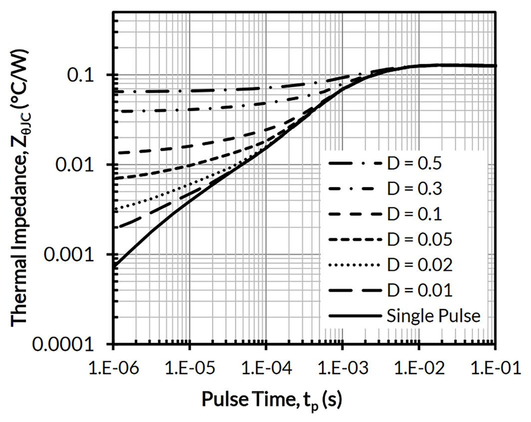
The maximum junction temperature (TJ,Max) figure for a SiC device and its current rating are essentially dictated by the packaging used. Despite the intrinsic material capability of SiC to operate safely at temperatures exceeding 500 °C, the
maximum is limited to 175 °C in the JFET of a cascode SiC FET. This restriction still allows SiC FETs to handle transient peak currents significantly higher than their continuous rating when initiated from lower temperatures. The transient thermal impedance plot for a specific die and package, such as the aforementioned SiC FET device, outlines these characteristics, as shown in Figure 1.
For instance, a single 100 µs pulse results in a transient increase in the junction temperature of about 0.015 °C per Watt of power dissipated. At approximately 10 ms pulse duration, the thermal impedance from junction to case approaches the steadystate value.
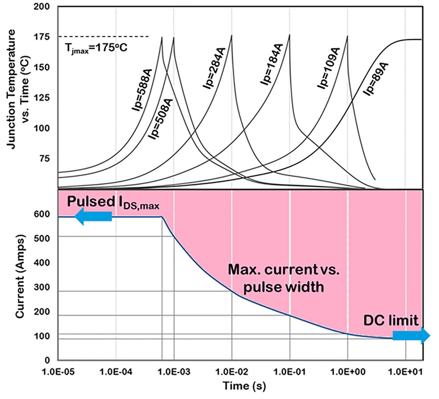
Practical implications for the sample SiC FET device are depicted in Figure 2 and Figure 3. In each scenario, the device case is soldered to a copper plane on a PCB with copper thermal vias through to a back-side aluminum heatsink held at 50 °C, separated by an insulating thermal interface material (TIM). Figure 2 illustrates that a thermal resistance of >1.2oC/W from junction to ambient may be expected, while the die and TOLL package determine the transient thermal response below approximately 1 ms. As depicted in Figure 3, with this arrangement, the continuous rating is 89
A device can handle up to 588 A peak current for a 500 µs single pulse before reaching TJ,Max of 175 °C.
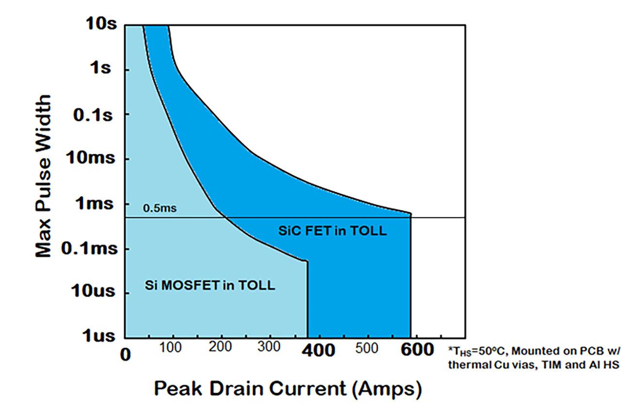
While SiC FETs showcase impressive results, a crucial question arises: how do they compare to Si-MOSFETs, commonly used in lower-power solid-state circuit breakers? The current squared through time (I2t) rating, a familiar measure for devices handling surge current, provides a compelling comparison. The sample SiC FETwithstands 588 A for 500 µs, while the Si-MOSFET rating stands at about 200 A, showcasing an ‘I2t’ difference of 8.6 times, as illustrated in Figure 4.
Beyond the evident safety margin provided by SiC FETs under overload conditions, there are further advantages. SiC FETs prove highly suitable for power conversion circuits with inductive loads, where voltage overshoot is expected. These devices exhibit robust avalanche capability and a 750V rating. Moreover, board-mounted DC-DC converters in servers and similar applications increasingly require a high peak power rating in a compact form factor, driven by data-intensive applications such as artificial intelligence (AI), machine learning (ML), and streaming.
Designs of these converters often assume that junction temperatures will approach their maximums due to peak currents experienced. Digital control, facilitated by sensors and prediction algorithms through PMBus™, provides junction temperature feedback, instructing the load to throttle back as needed to prevent the switch junctions from exceeding their absolute maximum. The ample margin
provided by SiC FETs instills confidence in the reliability and lifetime of the power system, potentially reducing the need for multiple paralleled devices and resulting in cost and board area savings.
Solid-state circuit breakers, designed to respond to high fault currents, can use SiC FETs and JFETs for their low voltage drop, displacing insulated-gate bipolar transistors (IGBTs), especially at lower current levels. The peak current rating of SiC FETs adds robustness to these breakers, allowing over-current detection circuitry to incorporate a longer delay before reacting. This attribute makes the circuit breaker more immune to nuisance triggering.
Compact SiC FETs with peak current ratings in the hundreds of amps emerge as ideal components for modern power conversion applications demanding high power density and peak load handling. Metrics affirm that these components outperform GaN and Si- or SiC-MOSFET parts in the same voltage class.

The big name in miniature components. The big name in miniature components.
Transformers & Inductors, DC-DC Converters, AC-DC Power Supplies
The most demanding applications require the world’s most reliable components. For over 50 years PICO Electronics has been providing innovative COTS and custom solutions for Military, Commercial, Aerospace and Industrial applications. Our innovative miniature and sub-miniature components are unsurpassed in any industry. PICO Electronics’ products are proudly manufactured in the USA and are AS9100D Certified.
To learn more about our products and how you can benefit from our expertise visit our website at picoelectronics.com or call us today at 800-431-1064.
TRANSFORMERS & INDUCTORS
Think Pico SmallOver 5000 std Ultra Miniature
• Ultra Miniature Designs
• MIL-PRF 27/MIL-PRF 21038
• DSCC Approved Manufacturing
• Audio/Pulse/Power/EMI Multiplex Models Available
• For Critical Applications, Pico Continues to Be the Industry Standard
DC-DC CONVERTERS
2V to 10,000 VDC Outputs — 1-300 Watt Modules
• MIL/COTS/Industrial Models
• Regulated/Isolated/Adjustable Programmable Standard Models
• New High Input Voltages to 900VDC
• AS9100D Facility/US Manufactured
• Military Upgrades and Custom Modules Available Surface Mount & Thru Hole Military • COTS • Industrial

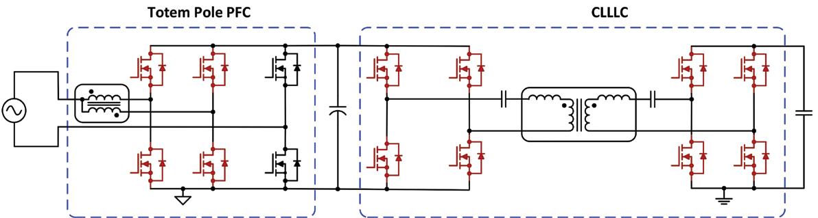
High-density power-conversion technology enablers using GaNA Sub-Terahertz 6G

Modern
electronics necessitate compact, high-efficiency power supplies that can economically convert AC grid power into a suitable form.Brent McDonald, Texas Instruments
HIGHswitching frequencies are among the most significant enablers for small size. To that end, gallium nitride (GaN) switches provide an effective means to achieve these high frequencies, given their low parasitic output capacitance (Coss) and rapid turn-on and turn-off times. However, the high-power densities enabled by GaN switches can often be amplified by using additional technologies such as integrated magnetics, advanced control techniques, and printed circuit board (PCB)-based transformers.
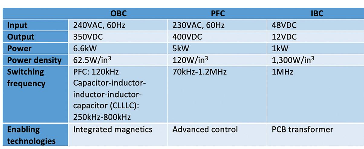
In this article, I will examine these technologies in three corresponding systems: the integrated magnetics inside a 6.6kW onboard charger (OBC) for an electric vehicle (EV), the advanced control methods used inside a 5 kW power factor corrector (PFC) for a server, and a smallform-factor PCB transformer inside a 1 kW intermediate bus converter (IBC) for a server. These examples use highperformance GaN field-effect transistors (FETs) to operate the power supplies at the highest practical frequency. Each power supply also uses a novel technology to get more performance out of the GaN FETs. The end result is a high-efficiency, small-form-factor design density that achieves more power in smaller spaces. Table 1 lists the specifications for the three design examples.
Integrated magnestics inside a 6.6 kW OBC for an EV
Figure 1 is a simplified schematic of an OBC [1] comprising two stages, both using high-performance GaN switches operating at a high frequency [2]. The first stage is a twophase totem-pole PFC.
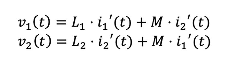
The coupled inductor used in the PFC works by using a single magnetic core for both windings. Equations 1 and 2 show the governing relationships between the winding voltages, currents, and inductances. In this design, L1 always equals L2.
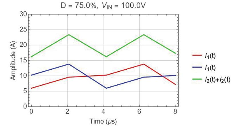
Sharing a common core for both phases reduces overall inductor volume by about 30% above and beyond what GaN can achieve on its own. Figure 2 shows the current waveforms for the two windings of the coupled inductor shown in Figure 1. The switching frequency of
each phase is 120kHz; however, because of coupling, the ripple current in each phase is 240 kHz. The objective of the design is to choose inductances L1/L2 and M so that the root-mean-square (RMS) currents in the windings are as small as possible. Additionally, since physical size is roughly proportional to the inductance, you also want the inductance to be small.
Figure 3 plots the RMS current in the winding as a function of the self-inductance (L1 and L2) and the mutual inductance (M). Notice that a minimum in the RMS current occurs when the mutual inductance is approximately –20µH. The dark blue dot denotes the ideal design point. This combination of self-inductance and mutual inductance yields a minimum RMS current with relatively small inductance values. I derived the
hatched area in Figure 3 from surveying practical, cost-effective designs from magnetics manufacturers. It turns out that, in practice, it’s not costeffective to achieve a coupled inductor in this region. As a result, I shifted the design to select the inductances corresponding to the red dot. This design point still captures the RMS current benefits from using a coupled
inductor without using large inductance values.
The second stage of the design uses a CLLLC topology for the DC/DC converter. This topology needs two inductors and a transformer. Designing the physical transformer such that the primary and secondary resonant

inductors are the leakage inductances of the transformer will achieve a smaller overall form factor. Using the first harmonic approximation helps
determine that the optimal inductances for this stage were a 14µH magnetizing inductance and a 2µH resonant inductance on the primary and secondary sides of the transformer. Operating the converter at 500 kHz to 800 kHz and integrating the inductors into a single physical structure with one core resulted in almost a 50% reduction in size compared to a state-ofthe-art discrete solution (reference [3] offers more details about the design).
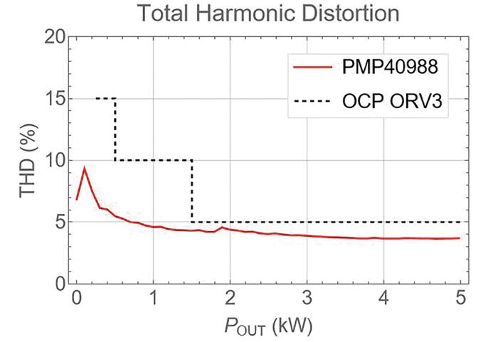
The two-phase, 5kW transition mode PFC for a server [4] operates with variable frequency to achieve zero voltage switching (ZVS) and a high-power factor at all operating points. To achieve this while keeping the overall size small, the operating frequency of the two phases varies between 70 kHz and 1.2 MHz. GaN is necessary to support the high switching frequencies [5]; however, you also need the advanced control techniques described in [6] to achieve ZVS and low total harmonic distortion (THD).
Figure 4 shows the topology for the power stage.
To achieve ZVS on every switching cycle — and simultaneously achieve low THD — the design uses a zero-voltage
detection (ZVD) signal produced by the GaN switches [5]. This ZVD signal reports to the controller if the switches turn on with or without ZVS. With this information and the solution to the state plane for the FET resonant transitions, you can solve for the ideal timing to achieve ZVS on every switching cycle while also having an excellent power factor. Figure 5 illustrates this control.
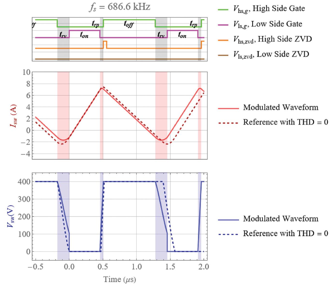
Figure 6 shows the operating waveforms when the applied frequency is too low (left), ideal (center), and too high (right). You can see that both ZVD signals are present only when the applied frequency is at the ideal value; thus, varying the frequency until ZVD is achieved for both FETs will reveal the ideal operating point.
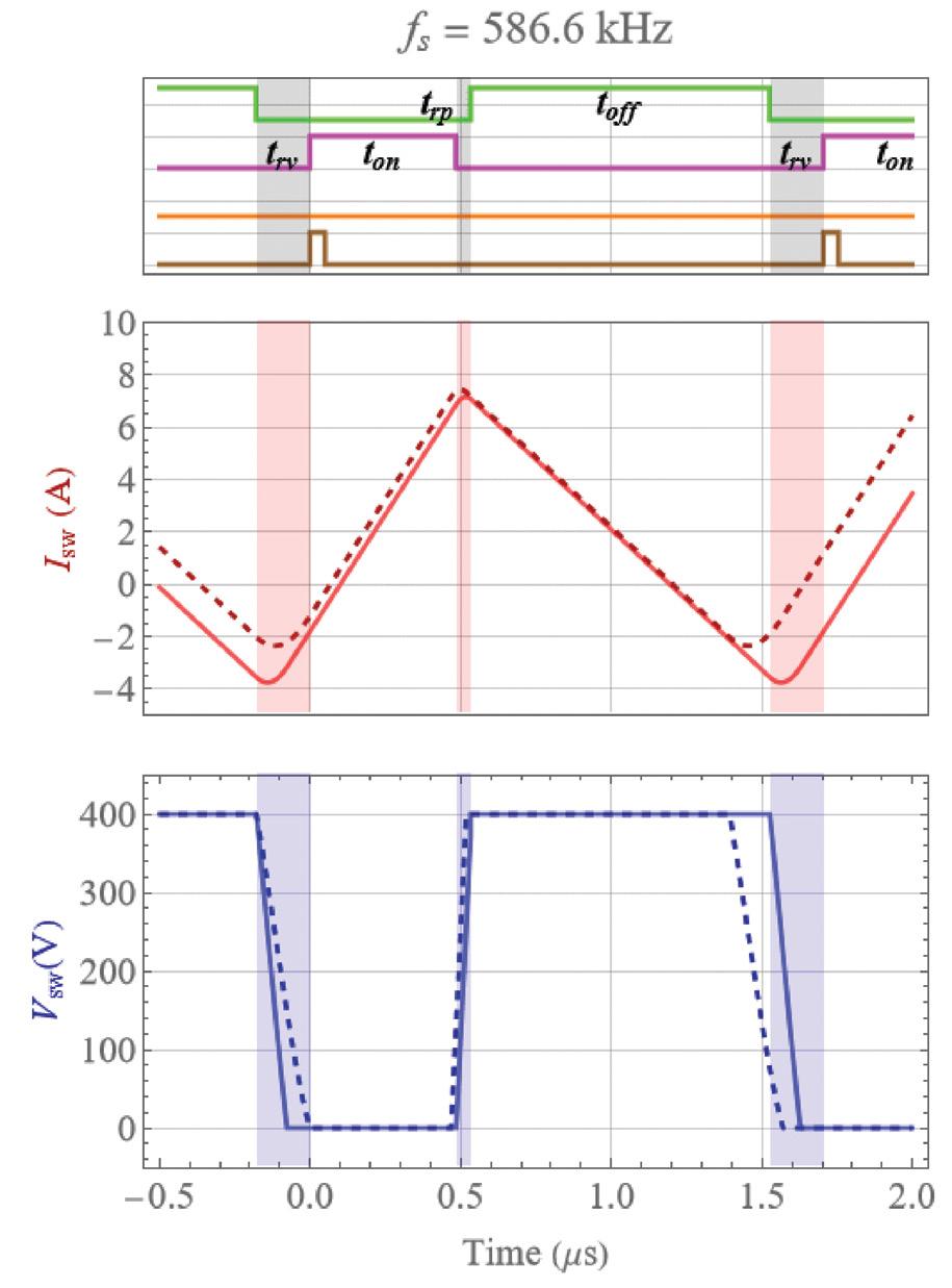
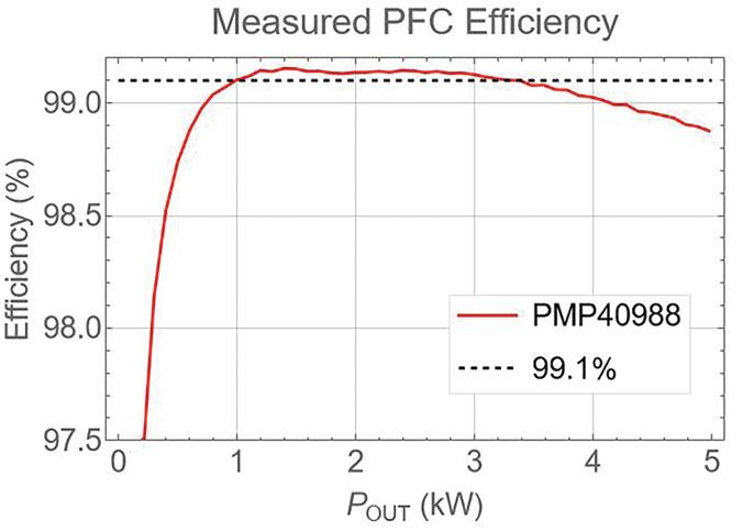
The ZVD signal, along with an accurate control law derived from the state plane, results in both high efficiency and very low THD, as shown in Figure 7.
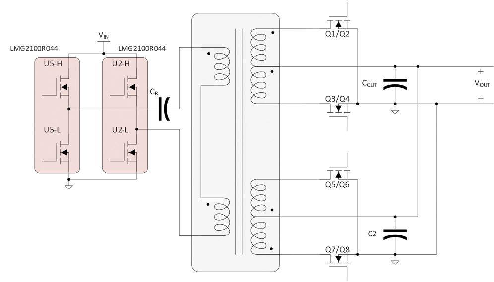
The final design example is a transformer in a high-density, 1 MHz, 1 kW oneeighth-brick inductor-inductor-capacitor (LLC) converter with an efficiency of over 98%. Like the first two examples, this design also uses GaN to achieve fast turn-on and turnoff times with low Coss [7]. An integrated PCB-based transformer eliminates the interconnect losses and reduces the size by wrapping the core around the PCB. Figure 8 is a schematic of the power stage and transformer structure.
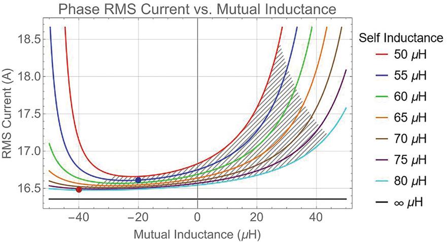
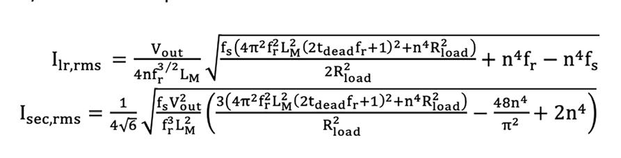
Table 2 shows the tank parameters chosen for this design (for details on selecting these parameters, see references [7-9]). Most losses in the converter come from the RMS currents, thus requiring an accurate method to estimate the RMS currents in the transformer windings. The method
presented in reference [10] does this by assuming that the magnetizing current stays constant when the converter operates at a switching frequency slightly below that of the resonant tank. With this assumption, creating a piecewise linear approximation of the LLC converter waveforms is possible. From these piecewise linear definitions of the current, you can derive the closed-form expressions of the RMS current for the transformer primary current and transformer secondary current, as shown in Equations 3 and 4.
To approximate the losses, you must
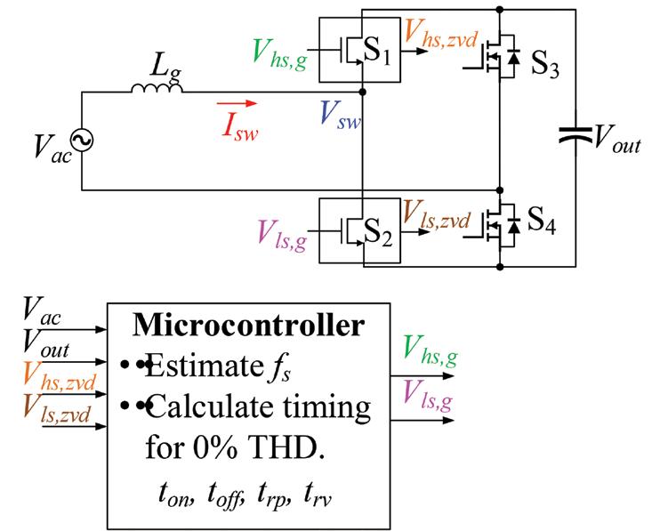 Figure 4. Two-phase PFC topology.
The ZVD signal, along with an accurate control law derived from the state plane, results in both high efficiency and very low THD, as shown in Figure 7.
The final design example is a
transformer in a high-density, 1 MHz, 1 kW one-eighth-brick inductor-inductorcapacitor (LLC) converter with an efficiency of over 98%. Like the first two examples, this design also uses GaN to achieve fast turn-on and turnoff times with low Coss [7]. An integrated PCB-based transformer eliminates the interconnect losses and reduces the size by wrapping the core around the PCB. Figure 8 is a schematic of the power stage and transformer structure.
Table 2 shows the tank parameters chosen for this design (for details on selecting these parameters, see references [7-9]).
Most losses in the converter come from the RMS currents, thus requiring an accurate method to estimate the RMS currents in the transformer windings. The method presented in reference [10] does this by assuming that the magnetizing current stays constant when the converter operates at a switching frequency slightly below that of
the resonant tank. With this assumption, creating a piecewise linear approximation of the LLC converter waveforms is possible. From these piecewise linear definitions of the current, you can derive the closed-form expressions of the RMS current for the transformer primary current and transformer secondary current, as shown in Equations 3 and 4.
To approximate the losses, you must first estimate the DC resistance of the winding by calculating the difference between an exact planar winding arc and a DC finite element analysis (FEA) model for the actual winding geometry. Equation 5 shows the resistance formula for an exact planar arc: where is the conductivity of copper, is the copper layer thickness, r1 is the inner radius of the arc, and r2 is the outer radius of the arc.
Figure 9 compares the DC FEA model for a circular arc and the exact winding geometry. Using only one-fourth of the model reduces the computational complexity. R+ and R– are two independent

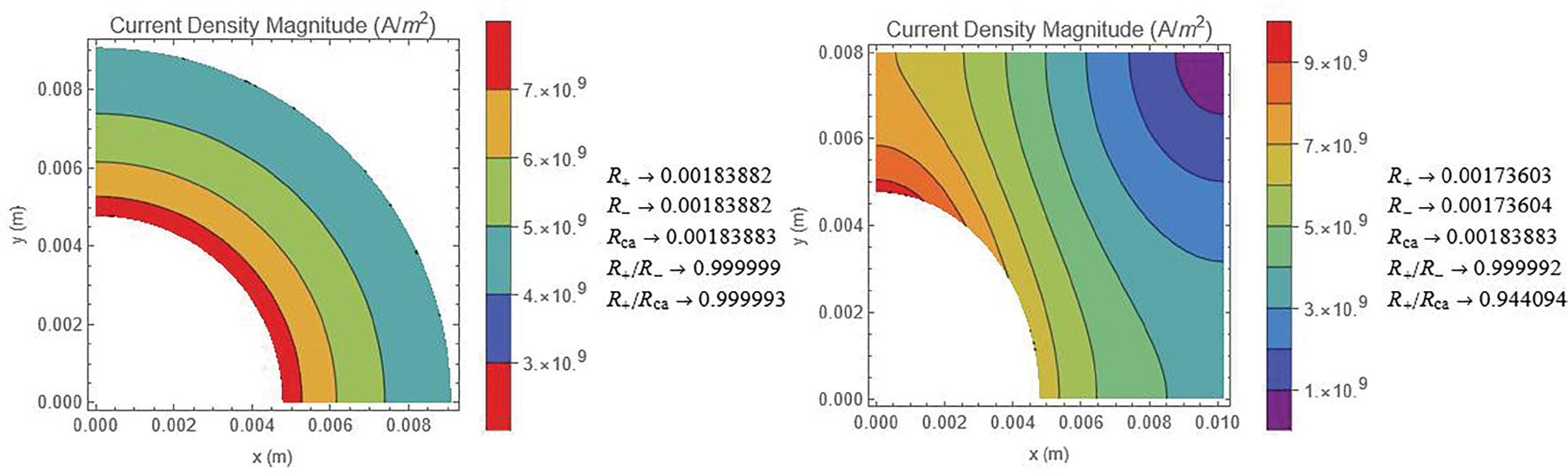
first estimate the DC resistance of the winding by calculating the difference between an exact planar winding arc and a DC finite element analysis (FEA) model for the actual winding geometry. Equation 5 shows the resistance formula for an exact planar arc: where is the conductivity of copper, is the copper layer thickness, r1 is the inner radius of the arc, and r2 is the outer radius of the arc.
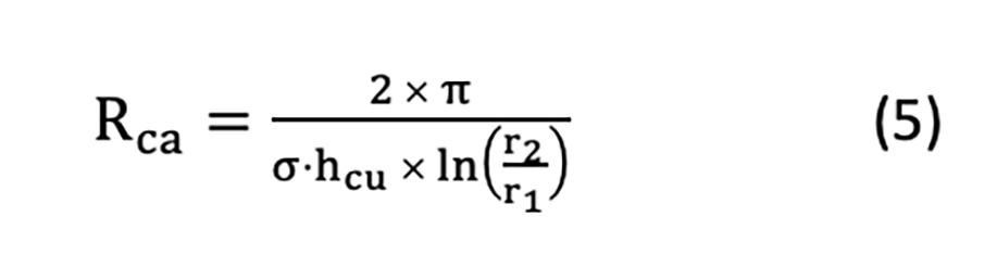
Figure 9 compares the DC FEA model for a circular arc and the exact
I collected this data with a 48 V input constant-current load and forced air. Figure 11 also shows the module efficiency and compares the predicted and measured losses.
GaN switches can increase the power density of various applications by enabling faster switching frequencies. The addition of technologies such as integrated magnetics, advanced control algorithms, and PCB-based magnetics, can significantly reduce the footprint of a power supply even further, achieving more power in smaller spaces.
winding geometry. Using only one-fourth of the model reduces the computational complexity. R+ and R– are two independent calculations of the winding resistances from the FEA model results; Rca is the output of Equation 5. The left plot calibrates the FEA model against Equation 5. The right plot determines the error between Equation 5 and the actual geometry. Using this error as a scale factor enables an adjustment of the model to correlate more closely to the real geometry.
Equation 6 is the final winding loss equation with the calibration and AC loss (including the influences from reference [11]): where fs is the switching frequency and is.
Ansys FEA software can check the transformer winding losses under transient excitation from the simulated LLC converter waveforms. Equation 6 matched the Ansys transient FEA model to within 1%.
Figure 11 illustrates the measured losses and efficiency from the hardware.
[1] Texas Instruments. n.d. “GaN-Based, 6.6-kW, Bidirectional, Onboard Charger Reference Design.” Texas Instruments reference design No. PMP22650. Accessed Jan. 22, 2024.
[2] Texas Instruments. n.d. LMG3522R030-Q1 automotive 650-V 30-mΩ GaN FET with integrated driver, protection, and temperature reporting. Accessed Jan. 22, 2024.
[3] McDonald, Brent, and Markus Zehendner. “Optimizing GaN-Based High-Voltage, High-Power Designs.” Texas Instruments Power Supply Design Seminar SEM2500, literature No. SLUP412, 20212022.
[4] Texas Instruments. n.d. “VariableFrequency, ZVS, 5-kW, GaN-Based, TwoPhase Totem-Pole PFC Reference Design.” Texas Instruments reference design No. PMP40988. Accessed Jan. 22, 2024.
[5] Texas Instruments. n.d. LMG3526R030
650-V 30-mΩ GaN FET with Integrated Driver, Protection and Zero-Voltage Detection. Accessed Jan. 22, 2024.
[6] McDonald, Brent, Sheng-Yang Yu, Branko Majmunovic, Johan Strydom, and John Kim. “A ZVD Control-Based 5kW iTCM Totem-Pole PFC for Server Power.” Published in 2023 Applied Power Electronics Conference and Exposition (APEC), March 19-23, 2023, pp. 2009-2013.
[7] Texas Instruments. n.d. LMG2100R044 100-V 4.4-mΩ half-bridge GaN FET with integrated driver and protection. Accessed Jan. 23, 2024.
[8] Huang, Hong. “Designing an LLC Resonant Half-Bridge Power Converter.” Texas Instruments Power Supply Design Seminar SEM1900, literature No. SLUP263, 2010-2011.
[9] Lu, Bing, Wenduo Lu, Yan Liang, F.C. Lee, and J.D. van Wyk. “Optimal Design Methodology for LLC Resonant Converter.” Published in 21st Annual IEEE Applied Power Electronics Conference and Exposition (APEC), March 19-23, 2006.
[10] Liu, Ya. 2007. “High Efficiency Optimization of LLC Resonant Converter for Wide Load Range.” Master’s thesis, Virginia Polytechnic Institute and State University.
[11] Dowell, P.L. “Effects of Eddy Currents in Transformer Windings.” Published in Proceedings IEE (U.K.) 113, no. 8 (August 1966): pp. 1387-1394.
Jami Brownlee jbrownlee@wtwhmedia.com 224.760.1055
Jim Dempsey jdempsey@wtwhmedia.com 216.387.1916
Mike Francesconi mfrancesconi@wtwhmedia.com 630.488.9029
Courtney Nagle cseel@wtwhmedia.com 440.523.1685
Jim Powers jpowers@wtwhmedia.com 312.925.7793
Publisher Mike Emich memich@wtwhmedia.com 508.446.1823
Managing Director Scott McCafferty smccafferty@wtwhmedia.com 310.279.3844
EVP
Marshall Matheson mmatheson@wtwhmedia.com 805.895.3609
CFO
Ken Gradman kgradman@wtwhmedia.com 773.680.5955


This inaugural event provides a unique platform for manufacturers to engage with industry leaders, technology experts, and peers who are navigating the complexities of digital transformation. Participants will gain invaluable insights into strategies, emerging technologies, and best practices that are reshaping the manufacturing landscape. From implementing Industry 4.0 solutions to leveraging data analytics and smart technologies, the forum delves into strategies that can redefine manufacturing processes and elevate operational excellence.
• Connect with manufacturers, engineers, and industry leaders
• Gain insight on digital transformation trends, technologies, and strategies
• Learn from experts who are now digitally transforming their manufacturing
• Hear and share lessons learned with manufactures across industries


Sponsorship opportunities are available for future Digital Transformation Forum programs. For more information, contact Colleen Sepich. 857.260.1360 | csepich@wtwhmedia.com
WITHOUT THE RIGHT POWER SOLUTION IT MAY AS WELL BE A COAT RACK.

As the #1 power supply distributor in North America, Sager Electronics offers 30,000+ world-class AC/DC and DC/DC power supplies and the widest range of modular solutions from over 30 leading manufacturers. Through its specialized group, Sager Power Systems, a dedicated team of highly trained, technically experienced power sales engineers work with customers to evaluate and specify standard and value-added solutions – each tailored to achieve a balance between performance, reliability and cost. Sager is Perfecting Power.
