


Deliver safe, reliable, efficient, affordable systems to market faster with Allegro’s sensing and power solutions.
INNOVATIVE SENSING AND POWER TECHNOLOGY FOR A SAFER, MORE SUSTAINABLE FUTURE

Allegro’s integrated circuits enhance power conversion, enable robust protection in harsh conditions, and reduce energy loss and thermal dissipation...so you can charge ahead in clean energy innovation. allegromicro.com/cleanenergy

20 Quantifying embedded MCU energy consumption
There is an intricate world of MCU energy efficiency benchmarks where the power of tasks meets the precision of micro Joules.
24 Harnessing nature’s gift: the normally-off D-mode GaN platform
GaN power semis are a hot topic in power electronics and two transistor variations prevail today: cascode GaN and E-mode GaN
29 How SiC MOSFETs and Si IGBTs boost sustainability in green energy systems

Both technologies offer energy conversion efficiency, reduced losses, and greater system reliability for the grid — but there are tradeoffs.
32 Designing online uninterruptible power supplies architectures, MOSFETs and drivers
The key to success lies in the adoption of technologies like discrete SiC and modern topologies to craft small, yet highly efficient single online UPS designs.


Today’s electronic engineers are challenged by multiple factors. Research over the years has illustrated common trends that you, as engineers, deal with including keeping your skills up-to-date, shrinking time-to-market windows, fewer engineers and smaller design teams for large projects and evolving technological trends. The bottom line is that you must continually update your engineering knowledge base to be successful in your work.

Throughout 2023, we are presenting a series of online educational days where you can learn how to address specific design challenges, learn about new techniques, or just brush up your engineering skills. We are o ering eight di erent Training Days. Each day will focus on a helping you address a specific design challenge or problem. These are not company sales pitches! The focus is on helping you with your work.
AVAILABLE ON DEMAND
THERMAL MANAGEMENT
AVAILABLE ON DEMAND
EMI/RFI/EMC
AVAILABLE ON DEMAND DESIGNING FOR SUSTAINABILITY

AVAILABLE ON DEMAND
BATTERY MANAGEMENT
AVAILABLE ON DEMAND

MOTOR DRIVES DESIGN
OCTOBER 11-12
IOT DESIGN / WIRELESS


NOVEMBER 8-9
ELECTRIC VEHICLE DESIGN
DECEMBER 6
5G / RF DESIGN
For more information and to register for these webinars, go to: EETRAININGDAYS.COM
EDITORIAL
VP, Editorial Director Paul J. Heney pheney@wtwhmedia.com
@wtwh_paulheney
Editor In-Chief
Aimee Kalnoskas akalnoskas@wtwhmedia.com @eeworld_aimee
Senior Technical Editor Martin Rowe mrowe@wtwhmedia.com @measurementblue
Associate Editor Emma Lutjen elutjen@wtwhmedia.com
CREATIVE SERVICES & PRINT PRODUCTION

VP, Creative Services


Matthew Claney mclaney@wtwhmedia.com @wtwh_designer
Art Director Allison Washko awashko@wtwhmedia.com @wtwh_allison
Senior Graphic Designer Mariel Evans mevans@wtwhmedia.com @wtwh_mariel
Graphic Designer Shannon Pipik mevans@wtwhmedia.com
Director, Audience Development Bruce Sprague bsprague@wtwhmedia.com
VP, Digital Marketing Virginia Goulding vgoulding@wtwhmedia.com @wtwh_virginia
Digital Marketing Coordinator Francesca Barrett fbarrett@wtwhmedia.com @Francesca_WTWH
Digital Design Manager Samantha King sking@wtwhmedia.com
Marketing Graphic Designer Hannah Bragg hbragg@wtwhmedia.com
Marketing Graphic Designer Nicole Johnson njohnson@wtwhmedia.com
Webinar Manager Matt Boblett mboblett@wtwhmedia.com
Webinar Coordinator Halle Sibly hkirsh@wtwhmedia.com
Web Development Manager B. David Miyares dmiyares@wtwhmedia.com @wtwh_WebDave
Senior Digital Media Manager Patrick Curran pcurran@wtwhmedia.com @wtwhseopatrick
VIDEOGRAPHY SERVICES
Video Manager Bradley Voyten bvoyten@wtwhmedia.com @bv10wtwh

Videographer Garrett McCafferty gmccafferty@wtwhmedia.com
Videographer Kara Singleton ksingleton@wtwhmedia.com
PRODUCTION SERVICES
Customer Service Manager Stephanie Hulett shulett@wtwhmedia.com
Customer Service Representative Tracy Powers tpowers@wtwhmedia.com
Customer Service Representative JoAnn Martin jmartin@wtwhmedia.com
Customer Service Representative Renee Massey-Linston renee@wtwhmedia.com
Customer Service Representative Trinidy Longgood tlonggood@wtwhmedia.com
FINANCE
Controller Brian Korsberg bkorsberg@wtwhmedia.com
Accounts Receivable Specialist Jamila Milton jmilton@wtwhmedia.com
WTWH Media, LLC
1111 Superior Ave., Suite 2600 Cleveland, OH 44114

Ph: 888.543.2447
FAX: 888.543.2447
DESIGN WORLD does not pass judgment on subjects of controversy nor enter into dispute with or between any individuals or organizations. DESIGN WORLD is also an independent forum for the expression of opinions relevant to industry issues. Letters to the editor and by-lined articles express the views of the author and not necessarily of the publisher or the publication. Every effort is made to provide accurate information; however, publisher assumes no responsibility for accuracy of submitted advertising and editorial information. Non-commissioned articles and news releases cannot be acknowledged. Unsolicited materials cannot be returned nor will this organization assume responsibility for their care.
DESIGN WORLD does not endorse any products, programs or services of advertisers or editorial contributors. Copyright© 2022 by WTWH Media, LLC. No part of this publication may be reproduced in any form or by any means, electronic or mechanical, or by recording, or by any information storage or retrieval system, without written permission from the publisher.
SUBSCRIPTION RATES: Free and controlled circulation to qualified subscribers. Non-qualified persons may subscribe at the following rates: U.S. and possessions: 1 year: $125; 2 years: $200; 3 years: $275; Canadian and foreign, 1 year: $195; only US funds are accepted. Single copies $15 each. Subscriptions are prepaid, and check or money orders only.
SUBSCRIBER SERVICES: To order a subscription or change your address, please email: designworld@omeda.com, or visit our web site at www.designworldonline.com
POSTMASTER: Send address changes to: Design World, 1111 Superior Ave., Suite 2600, Cleveland, OH 44114


up in the pre-2000s era with a power electronics engineer for a father, my family’s first introduction to power and energy efficiency efforts was primarily analog. The word “vampire” was associated with a TV show called Dark Shadows; it had nothing to do with standby power back then. Still, we were taught to unplug cords from outlets when an appliance was not in use, and inspections of our progress or lack thereof were not uncommon. We learned early on about “natural” air cooling and warming as air conditioning was for the new, big houses, not our 250-year-old farmhouse that also lacked central heating. This involved the daily ritual of opening windows at night and turning on the gigantic attic fan to welcome the cool night air, then closing the shades as the hot summer sun began rising. My Dad’s workarounds for no heat other than a Franklin stove for most of my childhood…well, you engineers can probably imagine how “imaginative” he got with that. (No details here as the memory of Pennsylvania winters still brings up a bit of trauma.)
Even before the word came into common usage in the early 2000s, he taught us how to “hypermile” to maximize fuel efficiency in our very technologically straightforward used vehicles. Stretching out coasting was a personal favorite of mine because, really, why would you hurry to the red light ahead of you? If the car did have AC, you only used that at higher speeds because leaving the windows down in other than city-street environments caused enough drag to decrease fuel economy.
All of this made for a practical education in preparation for lay ahead. Now, even in the time of technological marvel (and some despair), we have entered an era where the world is grappling with climate change, resource scarcity, and the ever-increasing demand for electricity. The quest for more efficient, cleaner, and sustainable power solutions to energy challenges is paramount.
Electronics engineers who focus on power efficiency are at the forefront of these technological advances. As essential contributors who address these challenges, your task to design efficient and sustainable products means incorporating rapidly evolving and innovative technologies and approaches. The impact of these efforts brings us LEDs, low-power MCUs, energy-efficient
HVAC systems, solar-powered electronics, energy harvesting, high-efficiency power supplies, EVs, low-power wireless communications, data centers with energy-efficient cooling, efficient power management integrated circuits, green building automation, efficient solar inverters, and more.
Some of these examples are profiled not only in his handbook but pretty much sum up the bulk of EE World’s editorial content, from authoritative freelancers like Bill Schweber, Jeff Shepard, Rick Nelson, and Ken Wyatt. It also includes contributing articles from subject matter experts at key technology companies, some of whom have written here addressing critical technologies that can help to meet fundamental challenges electronics engineers face in designs that impact the environment, cost, performance, and sustainability of electronic devices and systems.
My early education in power and energy efficiency may have seemed rudimentary, but, like many of us, the opportunities to expand it now seem limitless. We hope our handbook inspires you to test those limits.

WEall know the race is on for electrification, whether through government mandates and incentives or consumers demanding green transportation solutions with higher performance, longer range, and more features. Car makers are responding aggressively to electrify their fleets. With brands like General Motors publicly stating that all GM vehicles will be emission-free by 2035, it seems carmakers are responding aggressively to the call to electrify their fleets.
Bidirectional power conversion presents a unique, creative opportunity for any power system designer. This concept offers both practical and innovative applications in conjunction with the intense R&D efforts around electrification.
Fast-charging infrastructure is a problem. Initial electric vehicle (EV) platforms were designed with 400 V batteries supported by 400 V charging infrastructure and 400 V auxiliary systems. Even before the first 400 V vehicles were launched, however, the industry was busy developing 800 V platforms, effectively splitting the market into two voltage categories.
Some industry estimates project that 800 V battery architectures will be designed into most EVs introduced between 2027 and 2030. Though based on our experience, Vicor believes the transition will be slower than expected and that we will support 400 V battery designs for the foreseeable future.
Historically, power systems designers have designed PDNs from left to right, from source to load across the sheet. It is a natural convention that designers have conformed to for decades. In essence, we have been “right-handed.” Imagine a world where we are ambidextrous, using both hands and moving left-to-right and right-to-left.
Modular power components now available to the designer provide two key attributes:
• They are effective and efficient “DC transformers”—that is, they provide a fixed-ratio DC-DC conversion
• They are inherently bidirectional
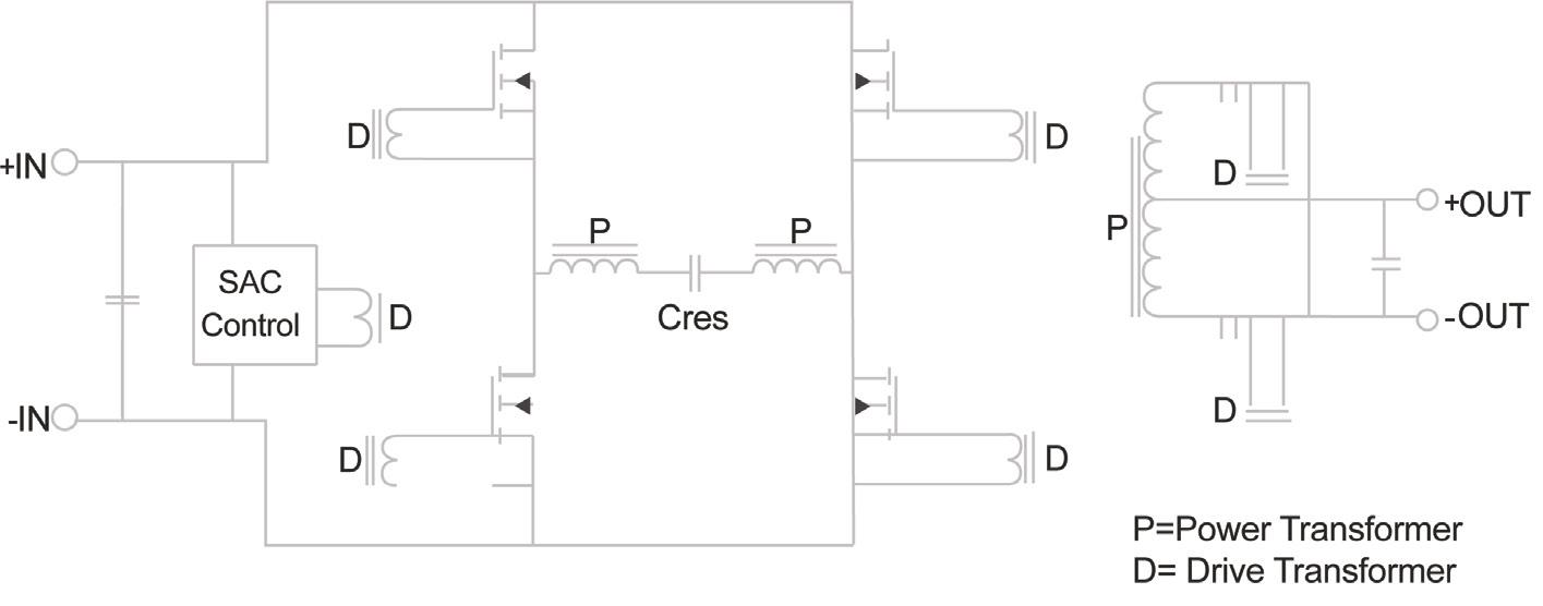
To tap into the promise of bidirectional PDNs, it’s important to understand how a Sine Amplitude Converter (SAC) operates by exploring the core enabling technology. Having abandoned left-to-right thinking, let’s start in the center, where there is a transformer and a series capacitor maintained in resonance with the transformer’s leakage inductance.
To one side, there is a switching bridge that, conventionally, would be viewed as an input stage chopping a DC bus, and to the other, an essentially identical arrangement that can be termed a synchronous rectifier. As long as those two paths switch synchronously with the resonant waveform in the central “tank,” the whole device is symmetrical and acts exactly like a DC transformer.
Voltage is stepped up according to the turns ratio of the magnetics, and current is stepped down—or vice-versa. Changes in impedance presented at one port are reflected at the other, and power will flow accordingly. Resonant, zero-voltage, and zero-current switching ensure low losses. Minimal stored energy in the resonant tank yields a good transient response through the converter, while MHz switching results in small, light inductors and capacitors.
Given the likelihood that 400 V and 800 V EVs will share the road for some time, the industry must grapple with the challenge of mixing the two architectures to ensure sufficient interoperability while avoiding consumer confusion and potential buyer backlash.
Interoperability between 400 V and 800 V systems, and conversely between 800 V and 400 V battery architectures, requires that the industry support all charging interfaces to assure drivers that their vehicles are compatible with any charging station. At the same time, we need to find novel ways of reusing legacy 400 V batteries, even as we improve 400/800 V system efficiency and extend and enhance vehicle-to-vehicle (V2V) and vehicle-to-other (V2X) charging capability.
This mix of voltage use cases can be complex. A 400 V battery connecting to an 800 V charger needs voltage boosting. An 800 V battery connecting to a 400 V auxiliary system requires voltages to be bucked down, while different V2V and V2X applications will likely demand a combination of both boost and buck conversion and regulation.
At Vicor, we contend that these power systems require high-voltage, bidirectional voltage conversion from 400 V to 800 V and 800 V to 400 V. EV charging stations serve as a good use case to illustrate the point. The vast majority of charging infrastructure in the US runs at 400 V, meaning that the industry would need to augment stations by upgrading or installing an 800 V option – a costly proposition. Installing an onboard bidirectional converter could easily solve this charging problem. Upon plugging in, the system would automatically detect whether the power needed to be bucked or boosted to charge seamlessly.
Given the coexistence of 400 V and 800 V EVs on the road, what options are there to harmonize these two distinct architectures?
Innovating with bidirectional power from V2X and beyond
New concepts like vehicle-to-grid (V2G) and vehicle-to-home (V2H) are being considered today. In most cases, varying levels of regulation are needed, but the power distribution networks (PDNs) are not overly complicated. In the context of V2G, the benefits of bidirectional power are multifaceted. V2G paves the way for improved grid stability and resilience. Electric vehicles can function as mobile energy storage units when connected to the grid. During periods of high energy demand or unexpected downtimes, these vehicles can supply power back to the grid, acting as a buffer and reducing the strain on conventional power sources.
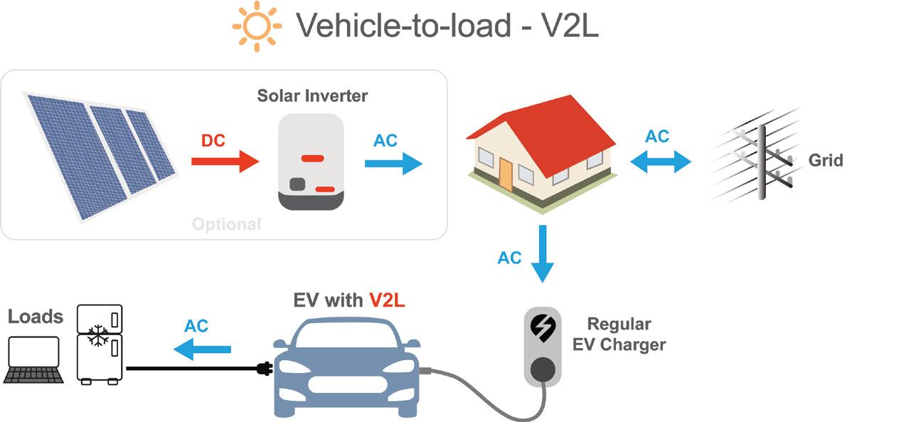
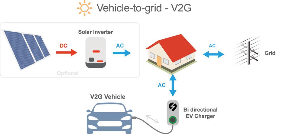
This ensures uninterrupted power supply and curtails the need for auxiliary power stations, often brought online during peak demand times, resulting in significant cost savings. Moreover, a new economic model emerges by allowing EV owners to sell excess power back to the grid. EV owners can monetize their stored energy, offsetting some of the costs of ownership and incentivizing the broader
adoption of EVs. Shifting the lens to V2H applications, bidirectional power heralds a paradigm of domestic energy independence and security. With the growing frequency of extreme weather events and associated power outages, having an EV with V2H capabilities can be a lifeline. In such scenarios, the home can draw power from the EV, ensuring that essential systems like heating, cooling,
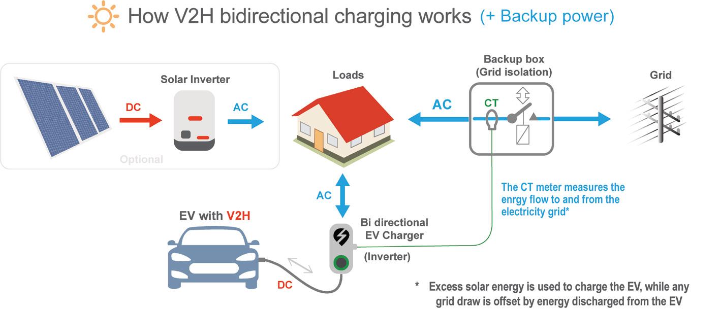
allowing homeowners to draw from their car’s battery during peak tariff periods and recharge during off-peak times, optimizing the cost of electricity.
Even more possibilities result from yet another option, vehicle-toload (V2L). V2L further accentuates the versatility of bidirectional power. Here, the EV becomes a portable power source capable of powering external devices, appliances, or systems. This is particularly useful in remote locations where access to a traditional power source might be challenging. Imagine setting up a campsite in a secluded area and using the EV to power lights and
or refrigeration remain operational. This transforms an EV into a backup power source, reducing a household’s reliance on the central grid or the need for separate, often fossil-fueled, generators. Over and above emergencies, on a day-to-day basis, V2H can lead to potential cost savings by
cooking equipment. Tradespeople and event organizers can also leverage V2L to power their equipment on-site, freeing them from the constraints of fixedpower sources and the inefficiencies of hauling bulky generators. The potential applications are vast, ranging from recreational to commercial.
Bidirectional power opens a myriad of possibilities. Solving the 400/800 V charging dilemma stands alone in terms of the priorities of today. But the other concepts are more than technological novelties. They represent a pivotal step toward a more integrated and sustainable energy landscape. By fostering grid resilience, promoting economic benefits for EV owners, ensuring domestic energy security, and enabling portability of power, bidirectionality harnesses the latent potential of electric vehicles, taking them from mere modes of transport to
pivotal nodes in the energy infrastructure of the future.
Voltage is stepped up according to the turns ratio of the magnetics, and current is stepped down—or vice-versa.

Changes in impedance presented at one port are reflected at the other, and power will flow accordingly. Resonant, zero-voltage, and zero-current switching ensure low losses. Minimal stored energy in the resonant tank yields a good transient response through the converter, while MHz switching results in small, light inductors and capacitors.
Two power component families best leverage bidirectionality. The Vicor Bus Converter Module, or BCM, offers isolated, fixed-ratio conversion between two voltage rails. The other is a non-isolated version, known as NBM, that is otherwise similar. The latter part is slightly easier to use in a bi-directional setting, as it will “start” (establish and stabilize resonant switching) from the power applied to either port. If isolation is necessary, using the BCM requires a small amount of additional circuitry to provide the bias to start it from the power applied to the “secondary.”
The promise of bidirectional power is underway in automotive. Two power component families best leverage bidirectionality capacity. The Vicor Bus Converter Module, or BCM, offers isolated, fixed-ratio conversion between two voltage rails. The other is a non-isolated version, known as NBM, that is otherwise similar. The latter part is slightly easier to use in a bi-directional setting, as it will “start” (establish and stabilize resonant switching) from the power applied to either
port. If isolation is necessary, using the BCM requires a small amount of additional circuitry to provide the bias to start it from the power applied to the “secondary.” For over 40 years, Vicor has established itself as the innovation leader in high-performance power module design, offering power designers the cutting-edge power topologies and
Figure 4. Sine Amplitude Converter Topology (SAC) provides isolation and voltage transformation functions, allowing you to place these functions where they are required, separating them from regulation.
architectures at the core of Vicor’s patented DC-DC power conversion products. Vicor’s revolutionary approach to power module design is well-suited to support future power conversion and distribution challenges.
References
New York Times, Oct. 1, 2021 Frost & Sullivan, Nov. 28, 2022
think...
• Ultra Miniature Designs
• MIL-PRF-27/MIL-PRF-21038
• QPL Approved DSCC
• Audio/Pulse/Power/EMI Multiplex Models Available

• MIL/COTS/Industrial Models
• Regulated/Isolated/Adjustable Programmable Standard Models
• New High Input Voltages to 900VDC
• AS9100D Facility/US Manufactured



• Military Upgrades and Custom Modules Available
Certified to AS9100D ISO 9001:2015 low profile from Call Toll Free: 800-431-1064 E Mail: Info@picoelectronics.com • FAX: 914-738-8225 143 Sparks Ave, Pelham, NY 10803 PICO Electronics Inc.
.18"
Surface Mount & Thru Hole Military • COTS • Industrial
INmechanics, it is obvious that moving parts wear under friction and the countermeasure is also clear: lubrication. Lubrication reduces friction and thus wear, or vice versa, extending service life.
Power electronic components are also subject to wear. Since this wear is based on thermomechanical processes that remain hidden from the eye, a frequently recurring set of questions arises:
• What is the reason that power semiconductors are limited in their service life?
• What is the biggest influencing factor?
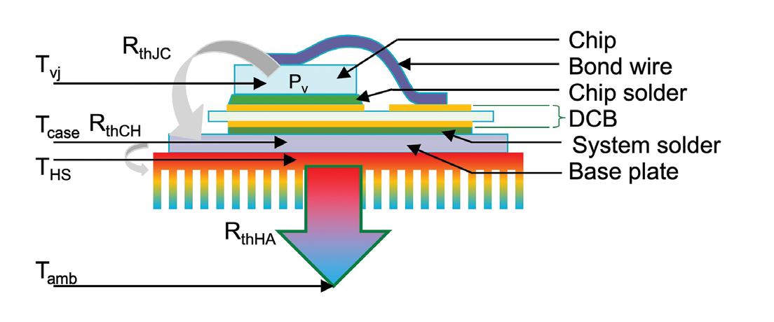
• How do you create a robust estimate of how long a semiconductor will last? The first two questions can be quickly answered by looking at a power semiconductor's structure, as given shown in Figure 1.
The structure consists of a ceramic laminated with copper on both sides, the socalled DCB (Direct Copper Bonding).
The DCB carries the semiconductor on its structured upper side. The chip itself is soldered on and connected to the surrounding structures by means of bond-wires. This structure is attached, also by soldering, to a base plate, which may be omitted for smaller components.
Figure 1 depicts how the heat generated by the chip is
Determining the durability and reliability of power electronics start with strategies for estimating the lifespan.
Dr. Martin Schulz, Littelfuse, Inc.Image: Adobe Stock Figure 1. Typical layer structure in power electronics
dissipated to the environment via the resulting thermal resistances. In the process, all layers of the structure heat up at different temperature levels.
Modern semiconductors now reach operating temperatures of up to 175°C, but heat sinks should not exceed a temperature of 85°C for reasons of burn hazard.
Liquid coldplates usually have a maximum inlet temperature of 65°C.
Since all the materials involved expand differently when heated, mechanical stresses arise between the layers as shear forces. These recurring stresses eventually lead to disruption (delamination) of the structure if the exposure time is long enough.
Especially In the case of bond-wires,
occasional use, but if used as a cab, its life is limited to 2-4 years. In fact, it may not be suitable for use as a horse-trailer tractor.
The key to answering the power semiconductor lifetime question, like that of the car, lies in the load profile of the application.
In principle, there is such a load profile for every electrotechnical application. This profile can be a forecast of solar radiation for installing a photovoltaic system or the local wind profile for the construction site of a wind turbine. Likewise, torque curves on machine tools, driving profiles of mobile applications, or charging curves for batteries come into question. Ideally, there is a precisely known individual profile. More often, however,
Regardless of the load profile, selecting a semiconductor must consider the blocking voltage and mechanical requirements, if any.
The load profile data can always be translated into a current profile, which allows a first selection of a power semiconductor.
another effect occurs. Their ends are firmly bonded to the underlying surfaces, but their length changes when the temperature changes. Because of the low thermal capacities, this heating takes place in the time range of a few seconds.
The length expansion causes microscopic movements and tiny angular changes at the mounting points and bends the wire. At the same time, the aluminum of the bonding wire expands differently than the crystalline structure of the chip; mechanical stresses occur between the so-called bond foot and the chip surface, which sooner or later leads to (dis) failure of the bond.
From the description of the failure mechanisms, the answer to the question of the driving parameter is immediately apparent: it is the temperature swing.
A power semiconductor can efficiently operate at a constant high temperature for extremely long periods. The same device, however, can fail quickly if the temperature constantly fluctuates by a high amount.
The last and most important question about a robust lifetime prediction is not so easily answered. It is like asking the question, "How long does a car last?"
It is easy to see that a vehicle can easily be used for 20 years as a second car with only
generic profiles that describe the application in its expected typical use are found.
A well-known example of such a generic profile is represented by the driving cycles that underlie the determination of the fuel demand of commercial vehicles.
The procedure's core is always the
solution of a linear equation, which also results from Figure 1. What is always sought is the chip temperature Tvj. This value is obtained from the power dissipation and the sum of the thermal resistances as a markup on the ambient temperature as seen in this equation for chip temperature (Figure 2).
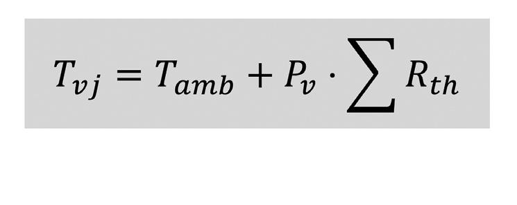
The expected power losses can be calculated using the electrical parameters current and voltage and the characteristics of the selected semiconductor. If the cooling is known with sufficient accuracy, or at least a maximum permissible heat sink temperature, the temperature swings at the chip’s junction can be estimated. As you can see in Figure 3, there are two steps describing how to get from load profile to temperature swing.
For technology series, semiconductor manufacturers have curves that correlate the possible number of cycles and the associated temperature swings. For Littelfuse IGBT modules based on solder-bond technology, the curve is shown in Figure 4.

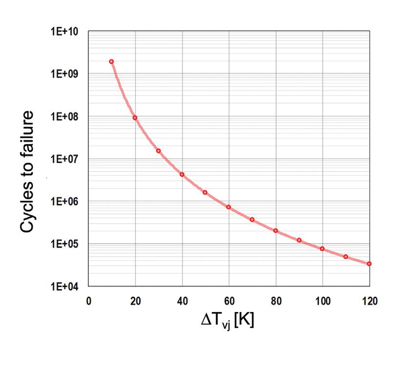

The design is successful if the load profile, temperature range, service life requirements, and number of cycles match.
If the service life is too short, various adjusting screws can be used to reduce the temperature swing:
• Selection of a more powerful semiconductor in the same package

• Selection of a design with lower thermal resistance

• Use of a heat sink with better heat dissipation
• Change from air cooling to liquid cooling
• Reduction of the switching frequency to reduce dynamic losses

Conversely, these levers can also help if the lifetime is too long. Although a reasonable reserve is to be welcomed, a service life prediction that is far too high can also be a sign of an oversized and, therefore, overly costly design.
The backward calculation
The load profile and the expected lifetime give a first impression of how many load cycles the semiconductor must withstand in the given application. Using the curve for cyclic load N=∫(DT) from Figure 4, an estimate of the tolerable temperature swing can be made from this.
Figure 5 shows how the maximum temperature deviation can be estimated directly from the load profile.
The temperature swing of 70K resulting from the diagram allows a maximum heat sink temperature of 55°C when a maximum of 125°C applies to the chip temperature.
Selecting a suitable semiconductor is then based on thermal resistance and power dissipation. Again, iteration is often necessary to determine the best matching component or to adjust the result in conjunction with a variation of the heat sink.
The relationship taken from Figure 5 already leads to a reasonably conservative design. The assumed 50 cycles per day include a comfortable margin. Additionally, the selected daily profile represents an unfavorable case that will not occur this way on most days.
If the cost situation permits, the conservative design is to be preferred.
Thin Film Resistor for Automotive RN73H
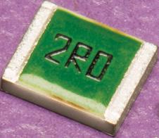
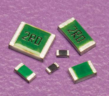
• Improved moisture resistance by special protective coating
• High precision tolerances

±0.05% ~ ± 1%
• High performance
TCR ±5 ~ ±100ppm/°C


To
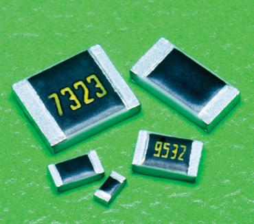
Surge & Pulse Precision Resistors SG73P/S




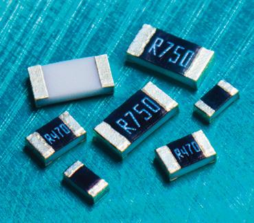
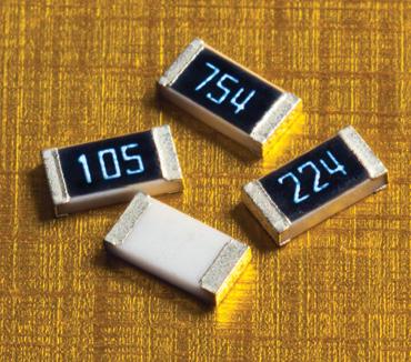
• Pulse withstanding; down to ±0.5% tolerance
• Endures the ESD limiting voltage


• Resistance range: 1 ~ 10MΩ
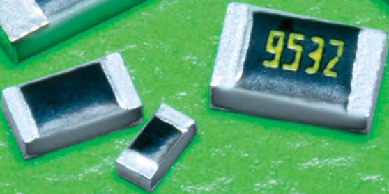
High Voltage Resistor for Automotive HV73V

• Maximum working voltages from 350V ~ 800V
• Resistance range: 10K ~ 51MΩ
• Tolerances:
±0.5% ~ ±5%
Anti-Sulfur Resistors - RT
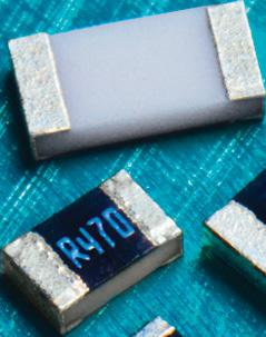
• Broad family of resistors with excellent anti-sulfur characteristics

• Passes ASTM-809


anti-sulfuration testing
• Excellent heat resistance and environmental resistance


companies are developing disruptive new technologies that move the world towards a safer and more sustainable future. Wide-bandgap semiconductors, notably GaN and SiC transistors, are a present-day example of a rapidly emerging and disruptive technology that dramatically improves power electronics systems' size, weight, and efficiency.
Both GaN-based and SiC-based transistors have lower gate capacitance and can, therefore, switch much faster than silicon-based alternatives. Power system designers can increase the switching frequency of wide bandgap transistors, thereby enabling smaller inductor sizes and reduced switching losses (higher efficiency) in power electronic systems. Additionally, wide bandgap devices can often operate at higher temperatures than silicon alternatives, enabling higher operating currents and/or reducing the size and cost of heat-sinking elements in power electronic systems.
As a result of these benefits, wide bandgap semiconductor devices are disrupting the power electronics industry. GaN and SiC technology underpin a more sustainable future with longer-range electric cars, higher-efficiency solar energy systems, and high-efficiency power supplies that reduce the electricity consumption of advanced and continuously operating data centers.
There is clear evidence that battery electric vehicles are adopting GaN technologies for their onboard chargers. Using GaN in such chargers reduces system size and weight, helping to improve the driving range and charging cost of electric vehicles. In the age of commuters seeking ever-increased EV range and lower charging costs and OEMs determined to deliver the features that car owners seek, these benefits are a big boost for business.
Gate drivers hold the key for efficient wide bandgap semiconductor adoption on the road to sustainability.
Mike Doogue and Vijay Mangtani, Allegro MicroSystems
A technical challenge concerns using SiC and GaN in power electronics systems. Compared to silicon transistors, wide bandgap devices are often harder to drive, control, and protect during normal operation and transient or short-circuit events. In many ways, system designers must trade off the complexity of driving SiC and GaN transistors to reap widebandgap transistors' efficiency, size, and weight benefits offered by a wide bandgap transistors.
If a short circuit event were to occur, a quick reaction time is essential to protect any component and system from catastrophe if a short circuit event occurs. GaN devices must be turned off incredibly quickly — within 0.1 µs — to protect the devices from damage. High-speed current sensors are often used to rapidly detect these types of short-circuit events. When Allegro's isolated gate drivers are coupled with high-speed current sensors, the safety of designers' systems is assured. Allegro's high-speed, lossless current sensor ICs reduce ohmic losses in a power electronics system and offer robust and accurate system control. These small form factor current sensor ICs include an integrated overcurrent comparator that responds to an overcurrent event in as little as 65 ns. This
from overcurrent events, offering a substantial risk mitigation benefit.
A typical gate driver design for a >400 V system uses 2 IC packages (an isolated gate driver and an isolated power supply), a transformer (discrete or integrated), and several passive discrete components. These components use valuable printed circuit board (PCB) space, and designers must contend with the interconnect's reliability and performance impact. These are conditions in which parasitic power loss is all but guaranteed, forcing engineers to try to compensate for the losses in various ways. This 2-chip solution is also far less efficient than it could be, as power density also suffers, so any power delivered to its destination may see a significant decrease from what designers envision and initially expect to occur. However, driving GaN and SiC transistors is becoming easier with the release of new, innovative, highly integrated isolated gate driver ICs, simplifying designs with smaller footprints and higher efficiency.
Gain a better perspective with GaN Integrating various active and magnetic components in a single semiconductorgrade package can minimize PCB space and interconnects, significantly reducing overall package size and increasing efficiency. With a much smaller footprint,
Recent developments in the electric vehicle industry demonstrate the benefits of a switch to GaN solutions, particularly in the onboard charger market. In one instance, a European charger OEM has delivered a notably smaller charging solution by opting for a GaN-based device, shrinking their onboard charger from approximately 30 Liters to 16 Liters. This significant volume reduction is associated with lower overall curb weight, which delivers better overall vehicular range. This feature is not only of increasing consumer demand but overall importance as EVs become more commonplace.
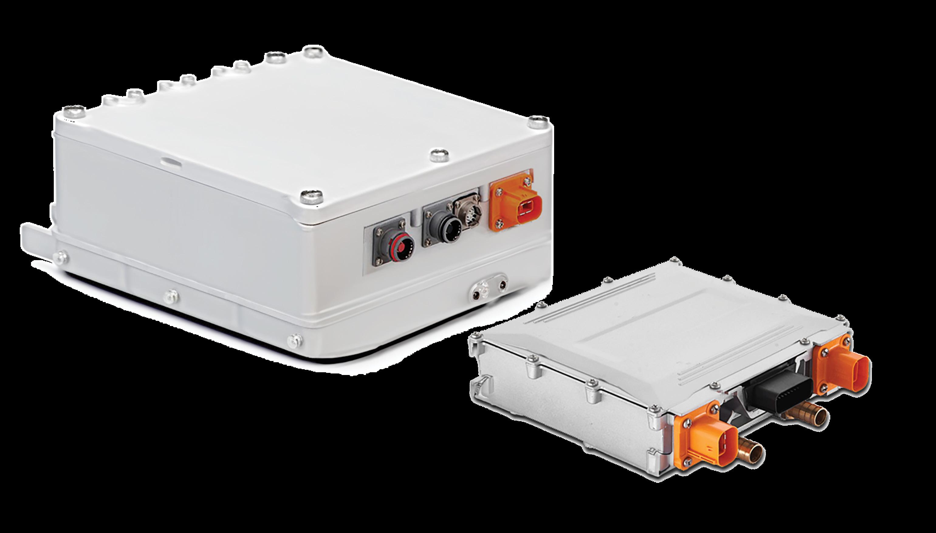
Companies developing disruptive, single-package, isolated gate driver ICs (with integrated inductor and DC/DC converter) that solves previously noted problems. These ICs boasts a small form factor, high power density, low common mode capacitance, and much lower Electromagnetic Interference (EMI) than typical drivers. Primary-to-secondary coupling capacitance of many isolated gate driver designs poses a significant challenge for wide bandgap power switches as they switch much faster than silicon power devices. Faster switching transitions create much higher dv/dt and increase common mode current transients, requiring additional efforts for EMI mitigation. The primary-to-secondary discharged at each switching instance, and the power loss is directly proportional
the capacitance between primary and secondary can reduce power losses and
Many common gate drivers have a primary-to-secondary capacitance of 8–10 pF or higher. However, with patented Power-Thru technology, Allegro's gate drivers reduce the primary-to-secondary capacitance to less than 1 pF, reducing
losses and simplifying
EMI compliance efforts. In a typical application, Power-Thru allows gate drivers to reduce power loss by more than 1 W per power switch and noise injection by more than 20 dB. In addition to its strong power and efficiency benefits, using fewer external discrete components in the AHV85110 leads to additional area savings at the PCB level. Allegro's highly integrated IC requires less than six external components, compared to 15 to 20 external components required when using competitor multi-chip devices.
The increase in system efficiency, reduction in used PCB area, and lower overall volume associated with innovative, highly integrated gate driver ICs can be substantial compared to multi-chip solutions. For example, a 22 kW onboard charger design using GaN transistors may require up to 32 isolated gate driver ICs and isolated DC/DC converters. A single-chip isolated gate driver IC using a single transformer for both the isolated voltage converter and isolated gate drive functions can reduce power loss between components.
In the case of the afromentioned 22 kW charger, highly integrated gate driver solutions offer demonstrable, significant efficiency benefits and space savings of 32x relative to conventional dual-chip ICs, which typically require 5 to 15 more external passive components.
Engineers in the automotive industry have expressed a strong belief that GaN drivers will be more broadly adopted soon. Additionally, many of the same engineers have indicated that the innovative, efficient, small form factor isolated gate drivers like the AHV85110 and AHV85111 may shape the future roadmap of power electronics systems in electric vehicles. With many applications and benefits, forward-thinking system designers in clean energy, data centers, and xEV markets should strongly consider incorporating isolated gate drivers into their designs.
 Figure 3: Consumers who choose electric vehicles can reap the benefits of GaN solutions through lighter vehicles with better range.

TOcomply with tightening regulations aimed at reducing energy consumption and achieving “Net Zero” targets, the global electronics industry must embrace new and innovative methods of designing efficient products that are also economical to manufacture. While GaN and SiC technologies have become a popular choice for enhancing peak efficiency, they have a limited impact during low-power modes where devices tend to operate most of the time. With a growing number of smart devices constantly connected to the internet during standby, poor efficiency at low power represents a significant source of waste.
In this article, we analyze some typical power supply efficiency profiles, how they influence overall efficiency in different usage scenarios, and explore a new approach that can deliver significant improvements without adding cost.
Darrel Kingham, CEO, PulsivWhy are traditional power supply designs inefficient at low power?
Converting AC to DC involves combining a boost PFC design and a flyback or LLC topology. Multiple variations and combinations are available to deliver a high-power factor and maximize peak efficiency, but they share a similar performance profile that compromises efficiency more dramatically as the load is reduced. In these graphs (published for commercially available power supply designs), the trend is clear:
• Performance at low load conditions is noticeably reduced as a direct result of losses in the series inductor used for power factor correction
• Maximum efficiency is not usually achieved until full load
• No data is reported below 10 - 20% of the load because the numbers are usually unimpressive
• The efficiency at 115 V is lower than 230 V, but the profile is similar
The electricity consumption of a product will vary depending on its typical operation and intended purpose, with most spending a small percentage of the time running at full power. A significant number of devices remain in standby mode, and all internetconnected products continue to perform necessary background tasks such as monitoring or updates even when not in use.
Kitchen appliances, for example, are typically used for relatively short periods of time and remain in standby mode for quick access. In contrast, smart TVs, games consoles, printers, & security cameras
provide continuous intelligent monitoring & remote-control features for consumer convenience.
Certain industrial products such as air conditioning units, factory equipment, and motor drives may have simple on/off control, operate at maximum power when used, or benefit from manual adjustment.
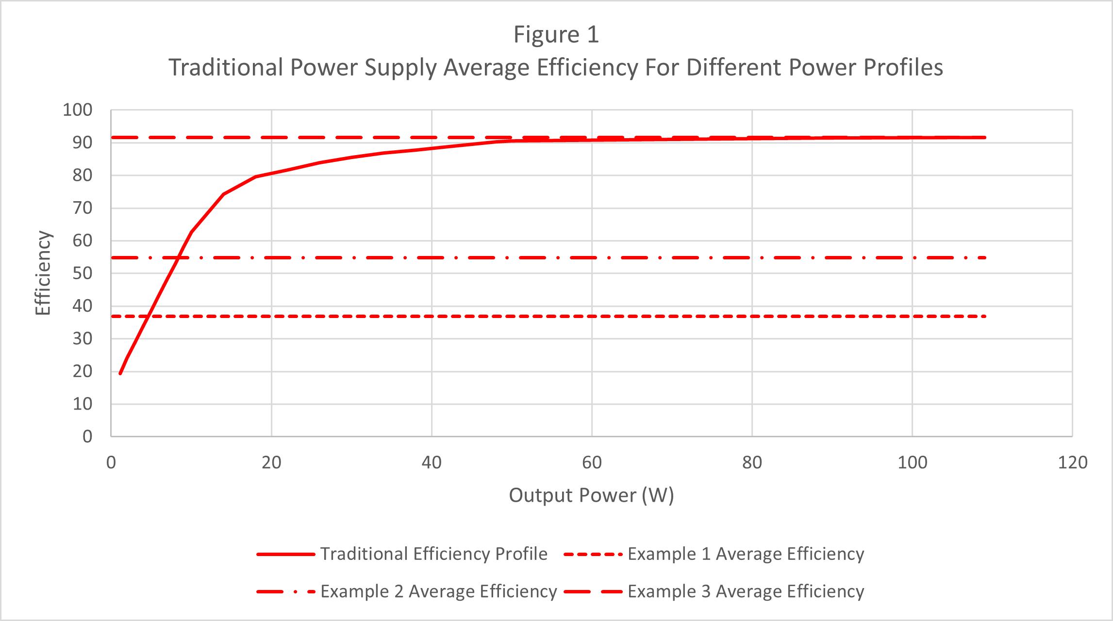
Figure 1 demonstrates the average efficiency of a product using traditional power supply technology, depending on how it behaves during normal operation.
Example 1 shows an average efficiency of just 37% when 80% of the time is spent in standby mode, 10% in lowpower mode, and 10% at full power.
Example 2 shows an average efficiency of just 50% when 50% of the time is spent in standby mode, 40% in low-power mode, and 10% at full power.
Example 3 shows an average efficiency of 91% when 100% of the time is spent at full power.
While the peak efficiency of a typical power supply may look impressive, this demonstrates the importance of understanding typical usage and the impact on overall average efficiency.
While GaN and SiC technology can help to improve peak efficiency in premium power supply designs, they do not change the general efficiency profile. It is possible to use multiple power supplies that handle conversion in different operating modes, but this involves added complexity and system cost. Pulsiv OSMIUM offers a new approach that delivers high efficiency at all times and maximizes the power available for meaningful work using a simple and economical design.
Pulsiv has designed, developed, and patented a new front-end AC-toDC power conversion method that delivers:
• High flat efficiency with 97.5% average, 99.5% peak, and 90% at just 2W
• 96% power factor
• Universal mains input voltage
• No inrush current
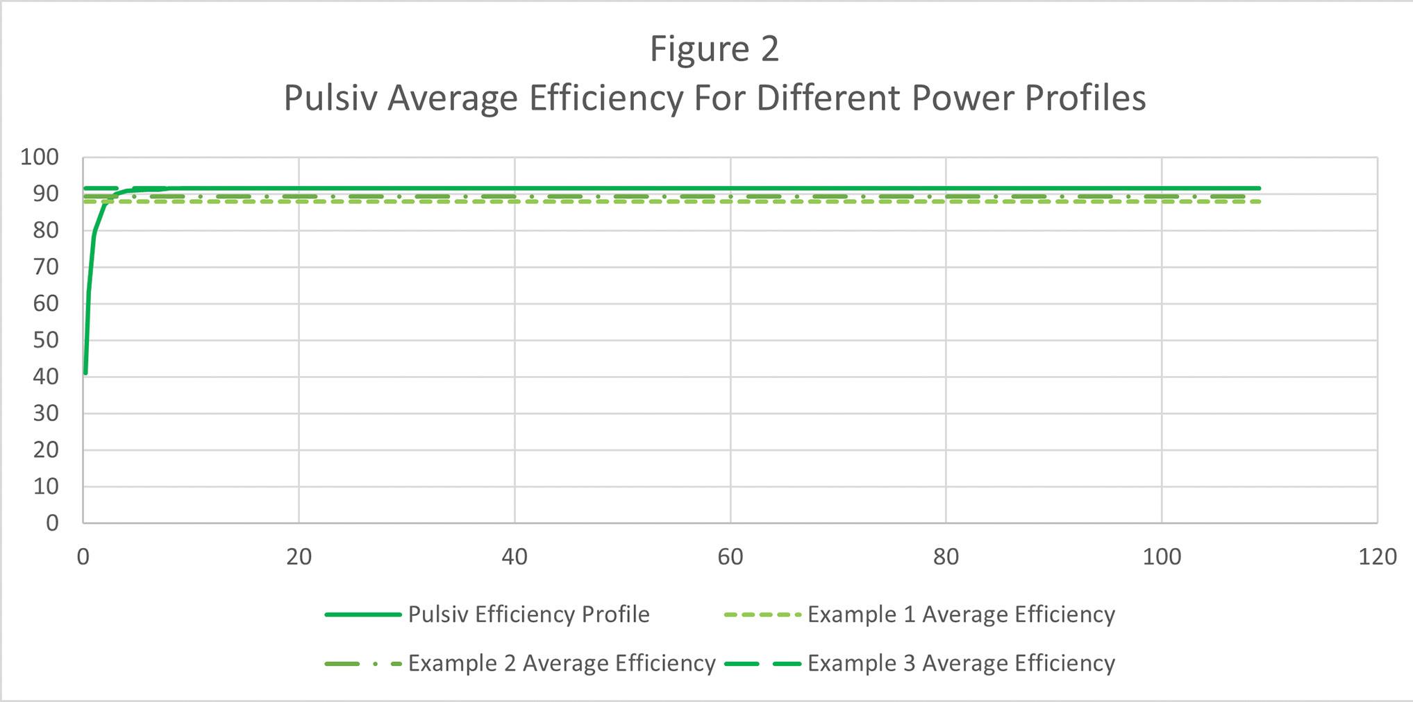
Figure 2 demonstrates a significant improvement in average efficiency when using Pulsiv OSMIUM technology paired with a quasi-resonant flyback. Under the same conditions:
Example 1 shows an average efficiency of 88% compared to the previous 37%
Example 2 shows an average efficiency of 89% compared to the previous 56%
Example 3 shows the same average efficiency of 91% without the complexity of
using an LLC.
Many governing bodies, such as The European Commission and the US Department of Energy (DOE), constantly drive manufacturers to improve efficiency and reduce energy consumption by setting minimum standards for different applications. As a result, they face an ongoing design challenge which typically involves adding system complexity, development time, and BoM cost. Engineers can avoid such compromises by combining Pulsiv OSMIUM technology with commodity flybacks to replace conventional LLC designs.
Pulsiv OSMIUM technology uses patented switching techniques to improve efficiency at low loads and therefore increase average
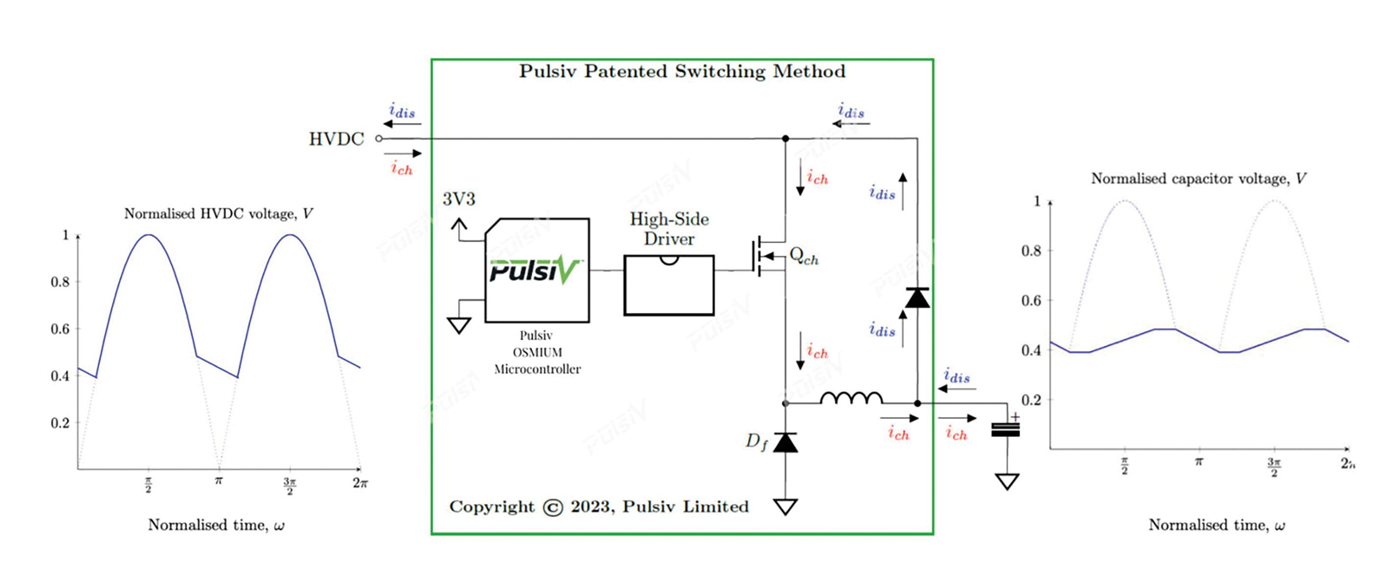
efficiency. Significant energy waste reduction is achieved by charging a parallel capacitor which replaces a lossy boost PFC inductor. The Pulsiv OSMIUM microcontroller manages the entire conversion process to ensure that just enough energy is available to ride through a period when the grid cannot support the load. The capacitor is then discharged by a follow-on dc-dc converter through a simple diode. The voltage on the storage capacitor is regulated to 150 V or 180 V (pin selectable), which means avoiding conventional 400 V larger and more expensive capacitors.
• Designed for use with SN6501 and SN6505B push-pull transformer drivers from Texas Instruments
• Low-profile, center-tapped design for isolated power supply
• 2500 Vrms, one minute isolation (hipot) winding to winding
• Ideal for DC-DC converters in EV/HEV applications
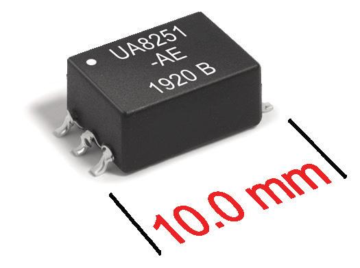

methods and benchmarks exist for quantifying the energy consumption of embedded microcontroller units (MCUs), and related energy consumption benchmarks for standard peripheral functions such as Bluetooth low energy and Wi-Fi. Over time, MCU designs have changed to support the demand for higher energy efficiency. In addition, there is another world of energy consumption benchmarks for servers (SPECpower — a benchmark for web servers running Java), data centers (Power Usage Effectiveness, PUE, international standard ISO/IEC 30134-2:2016), and other areas that are beyond the scope of this FAQ.
Energy consumption is different from power consumption. Power consumption for lowpower devices can be measured in milliwatts (mW), while energy consumption is often measured in micro Joules (µJ). Power consumption is most relevant with power sources such as rechargeable batteries that can only supply a few mW (milliamps, mA, of current) without damage. Drawing higher peak currents can permanently reduce a battery's capacity.
Energy consumption determines how much energy is drained from the battery to perform a given task. Energy consumption is the integral of the power consumption over the time needed to perform the operation. Since two variables are involved, the power consumption and the specific operation being performed, most energy consumption benchmarks specify one or a series of tasks to be completed and then provide a metric based on the µJ of energy needed to complete the defined tasks.
There are additional considerations when comparing the energy consumption of devices like the Internet of Things (IoT) wireless sensor nodes that spend a great deal of time in standby. For those devices, the total power consumed equals the active mode power plus standby (sleep) mode power plus wakeup power (Figure 1).
So, it's not just processing that consumes energy; waking up can consume significant amounts of wasted energy since the MCU cannot do any processing until all its digital and analog subsystems are fully awake and operational.
There is an intricate world of MCU energy efficiency benchmarks where the power of tasks meets the precision of micro Joules.
Jeff ShepardImage: Adobe Stock
For example, some systems wake up and use an on-chip ADC to sample a sensor input. In those cases, allowing time for slowersettling analog circuitry and quicker-settling digital circuitry is necessary. The wakeup characteristics of various analog elements often have a significant impact; voltage references or regulators and using external decoupling capacitors can take several milliseconds to settle. In some applications, an MCU can use just as much energy during wakeup as in active mode.
IoT and ULP
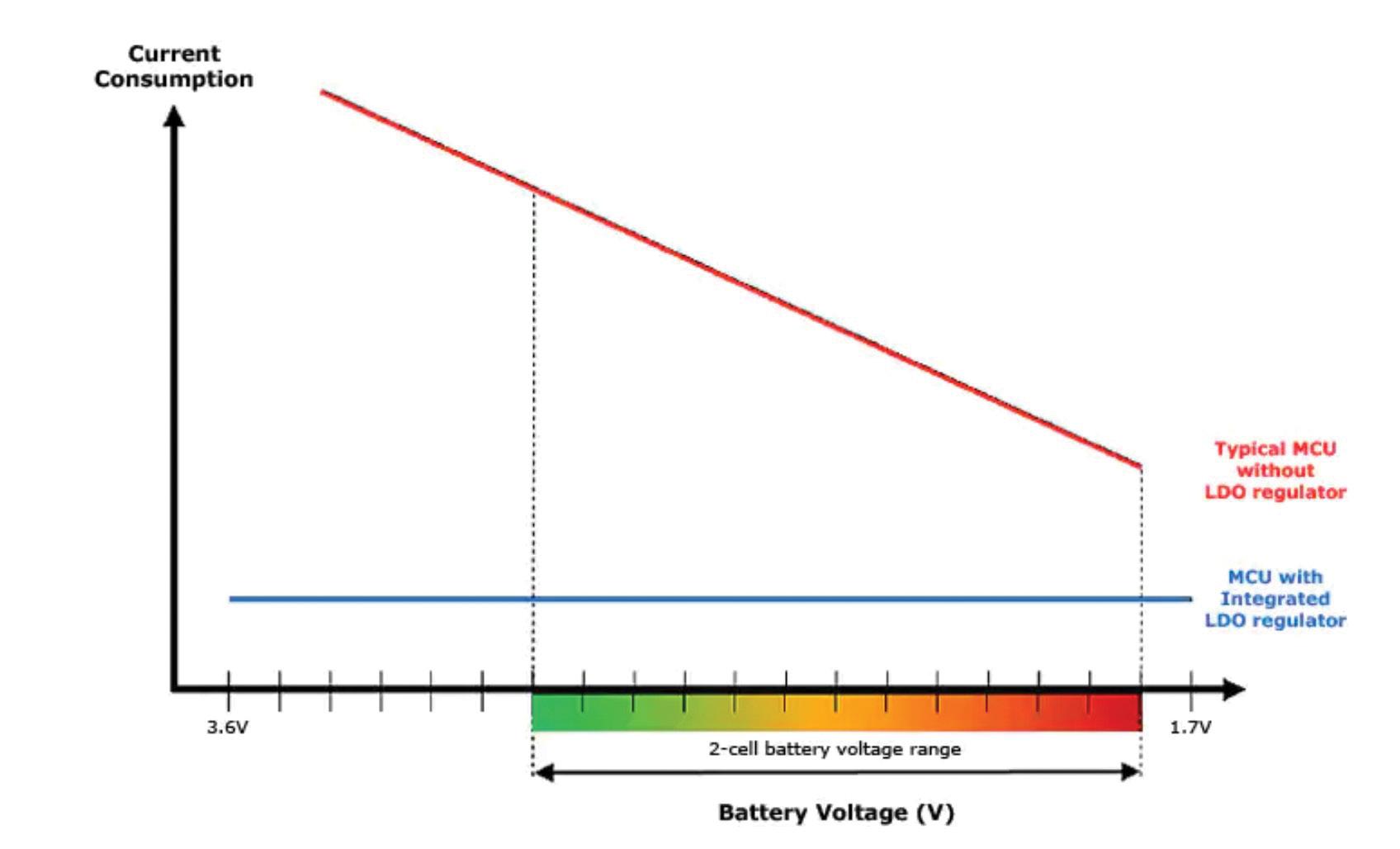
Ultra-low power (ULP) describes MCUs designed to run for up to 10 years on a single primary battery or from harvesting pico-Joules of ambient energy. ULP MCUs are particularly useful for wireless IoT nodes, wearables, and similar low-power devices. As shown above, total power consumption is a complex measurement that can make identifying the "best" MCU for a given application challenging. For example, energy harvesting-powered systems may benefit from the lowest active current requirement. But, for systems that spend most of the time in sleep/standby mode, quiescent current may be the critical parameter. Additionally, noncomputing elements such as integrated voltage regulators can impact MCU energy efficiency (Figure 2). An integrated low drop out (LDO) regulator can help significantly reduce power consumption. For example, a battery-powered MCU without an LDO regulator can consume up to 50% more power from fully charged batteries delivering about 3 Vdc, compared with depleted batteries delivering about 1.8 Vdc. Adding an integrated LDO results in a flat current consumption curve and reduced overall power consumption.

Founded by EDN in 1997, the mission of the EDN Embedded Microprocessor Benchmark Consortium (EEMBC) was to develop unified MCU performance benchmarks. When the
EEMBC became independent of EDN in 2012, the short-hand name, EEMBC, was kept. Today, the EEMBC ULPMark Working Group develops MCU power and energy analysis profiles and benchmarks. There are currently two profiles for deep sleep and one for active workloads:
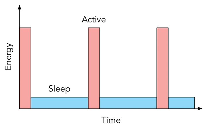
• ULPMark-CoreProfile benchmark also called the ULPMark-CP, measures the energy cost of deep sleep by focusing on the MCU core, specifically the energy cost in sleep and the transition to and from active mode. The Core Profile runs on a one-second duty cycle combining a common set of workloads (defined below) with an extended period of inactivity to enable microcontroller low-power modes (Figure 3).
• ULPMark-PeripheralProfile measures common peripherals' energy impact on deep-sleep by activating one or more of four peripherals in one of ten fixed configurations, called slots. The peripherals include:
• Real Time Clock (RTC)
• Analog-to-Digital conversion (ADC) at 1 Hz and 1 kHz
• Pulse-width Modulation (PWM) at 32 kHz and 1 MHz
• Serial Peripheral Interface (SPI)
• ULPMark-CM benchmark runs the classic CoreMark benchmark for active workloads. The active portion of the ULPMark-CP
benchmark runs for about 3% of the total runtime. It requires data saved during deep sleep through the so-called "retention RAM." Since a sleepy edge node is not expected to.clear its RAM after every sleep cycle, the exit- and enter-costs of retention RAM are designed to measure the true energy cost of sleep modes. During the active portion of the test, the benchmark implements the following workload (portable across 8-, 16-, and 32-bit MCUs):
• Generate 20 GPIO pulses
• Perform an 8-bit linear interpolation
• Perform a 16-bit integration (filter)
• Compute a 7-segment LCD binary conversion (saving state)
• Search for a substring in a string
• Perform a small bubble-sort
• Permute the bits of a string based on input and previous state
The various ULPMark benchmarks use formulas incorporating the reciprocal of the energy values measured in µJ to provide larger benchmark scores for reduced energy consumption (better performance).
ULPMark-CP benchmark score = 1000 / median energy consumption (5 runs of the benchmark for 10 seconds)
ULPMark-PeripheralProfile benchmark score = 10000 / median energy consumption (5 runs of the benchmark's ten slots, also for 10 seconds)
ULPMark-CM benchmark score = 1000 * (iterations / total energy in µJ)
In addition to the ULP benchmarks, EEMBC offers a suite of benchmarks for quantifying the energy efficiency of IoT edge devices. The IoTMark determines the combined energy consumption of an edge device consisting of a sensor, a processor, and a radio interface. The two benchmarks included in IoTMark are the IoTMark-BLE, a bluetooth low energy (BLE) benchmark, and the IoTMark-Wi-Fi, a Wi-Fi benchmark still under development.
Designers can use the IoTMark-BLE profiles to model an actual IoT edge node, including an MCU, an I2C sensor, and a BLE radio through sleep, advertise, and connected operation. The benchmark is structured to quantify the tradeoffs between the connection interval, frequency, and various sensor characteristics, with overall energy consumption.
The IoTMark-BLE benchmark uses the portable IoTConnect framework that supports any radio modules and MCUs and works with any software stack or embedded operating system. It's highly flexible with user-defined connection intervals, advertise intervals, I2C transmit size and speed, BLE transmission power, and other system characteristics.
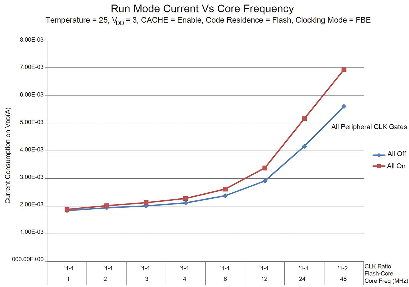
Power consumption is generally proportional to the operating frequency in processors of all types. At a given supply voltage, it's possible to specify current consumption / MHz of clock frequency, such as current consumption/MHz at 3V. In addition to slowing the clock frequency to decrease energy consumption, disabling unused peripherals can reduce the amount of energy an MCU consumes (Figure 4). It's also essential to use the correct clock speed for comparisons. Utilizing the instruction clock speed is more meaningful than using the system clock speed. System clocks often run at twice the instruction
Figure
benchmark operates in long periods of sleep, followed by a brief wakeup to perform minimal processing, mimicking an IoT edge node conserving energy. In this case, the wakeup energy is subsumed in the sleep time (Image: EEMBC).
execution speed, doubling the apparent operating efficiency.
The relationship between clock speed and current consumption is essential when optimizing system-level efficiency. Slowing the clock speed during periods of lower system load can save energy without negatively impacting overall system performance. Dynamically changing the clock speed on the fly can be effective, but it can also be challenging. With some MCUs, it's also necessary to adjust peripheral register settings dynamically to account for the changing clock speeds.
Maintaining the processor section in an MCU in a low-power state is usually the most effective way to save energy. For example, instead of waking up the processor to move data to and from various peripherals, the direct memory access (DMA) controller can be used. The DMA can effectively move data around in an MCU without the energy penalty from having the processor perform the same housekeeping function.
Additionally, some MCUs include lowpower peripherals dedicated to specific functions offloading activities from the processor. These peripherals can efficiently implement various common functions, including timing and measurement, straightforward user interfaces, safetyrelated monitoring, basic motor controls, and more, enabling the processor to remain in a low-power state for longer.
Energy consumption is an important consideration in many applications employing embedded MCUs. Benchmarking the relative performance of various MCUs is only one aspect of designing energy-efficient devices. Optimizing the connection interval, frequency, power, and other characteristics of wireless communications can be critical in IoT nodes. And general design considerations such as using DMAs and other peripherals to offload activities from relatively energy-hungry processors can lead to lower overall energy consumption.

From simple modifica�ons to high-complexity designs, ISO-cer�fied Sager Electronics specializes in solving problems. As a trusted advisor, we go beyond fulfillment to add value in the areas of power, ba�ery, thermal, connector and electromechanical for a wide range of markets and applica�ons. With quick-turn prototyping, product safety tes�ng, and assembly in the USA, our experienced team can guide you through the en�re engineering process – all with faster �me to market and higher reliability than a typical custom build.

WHEN AN OFF�THE�SHELF SOLUTION JUST WON’T DO, YOUR LATEST INNOVATION MAY AS WELL BE A LUNCHBOX.
GaN power semis are a hot topic in power electronics and two transistor variations prevail today: cascode GaN and E-mode GaN
Davide Bisi, Umesh Mishra, Philip Zuk, Transphorm, Inc.
WHENconfronted with the choice, the debate at times inexplicably leans toward E-mode. In reality, cascode GaN proves to be a fundamentally superior platform in performance, reliability, versatility, manufacturability, and practical application. The reasoning lies in the cascode’s ability to capitalize on the inherent advantages of the GaN material.
Nature’s gift from GaN: the 2DEG GaN transistors are successful primarily because of one key natural phenomenon: the 2-dimensional electron gas (2DEG) channel. The 2DEG is a high-speed channel that spontaneously forms at the interface between the GaN and a thin AIGaN layer. Its electron density is amongst the highest naturally occurring in semiconductors. It also offers high mobility at 2000 cm²/V·s, twice that of state-of-the-art silicon (Si) and silicon carbide (SiC) devices. As a result, the 2DEG yields an impressively low resistance-versuscapacitance figure of merit with record-high efficiency.
Every GaN power semi starts as D-mode device
Figure 1 shows the archetypal form of a lateral GaN power transistor, lateral being the structure of virtually every GaN device on the market today. The AlGaN/GaN layers are deposited on a silicon substrate and separated by an engineered buffer to achieve high material quality and blocking voltage. The channel is contacted by the source and drain terminals to enable current to flow between the source and drain contacts. The gate terminal modulating the current is located between the source and drain terminals and is isolated with a dielectric stack to ensure low leakage and high robustness. A field-plate structure is designed for best electric field spreading and highest reliability.
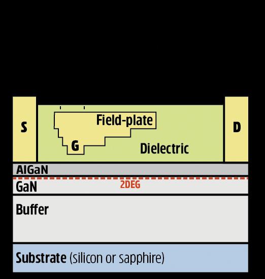
Thanks to the material’s nature, the 2DEG channel at the AlGaN/GaN interface forms spontaneously, with no need for external gate bias. This means the device is normally on and requires a negative gate bias to deplete the channel and
turn off. It is, in fact, a depletion mode (D-mode) device. However, power electronic systems require normally-off devices for fail-safe operations.
The question then becomes how to make the lateral GaN HEMT normally off. This is where cascode and E-mode (p-GaN gate) technologies part ways.
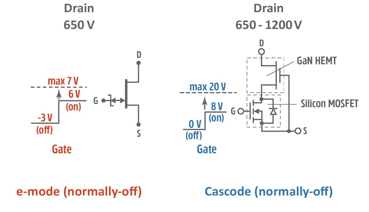
In the cascode technology, the GaN HEMT is untouched to retain its highest performance and reliability. In its natural state, the 2DEG channel is free to maximize its unparalleled combination of high mobility and charge density. Transphorm’s cascode approach pairs the GaN HEMT with a low-voltage, normally-off Si MOSFET to achieve normally-off operation. This solution provides
a positive threshold voltage of 2.5 V to 4.0 V, depending on power level, topology, and system architecture.
Alternatively, an E-mode approach opts to control the 2DEG channel inside the HEMT itself—a design decision that negatively impacts the 2DEG’s advantage.
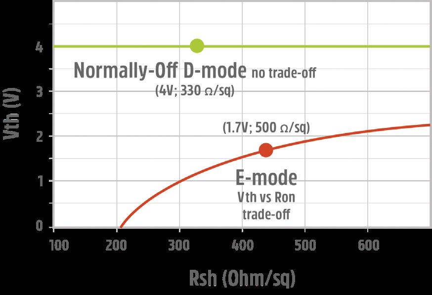
Critical compromises are made when power engineers modify a lateral GaN HEMT to achieve normally-off behavior. First, the 2DEG’s charge density must be reduced, which generates a higher resistance per unit area [Figure 2] and lower figure of merit than achieved in its natural state.
Second, a p-type doped GaN layer [Figure 3] must be added under the gate metal. The p-GaN layer serves as a built-in negative battery (approximately -3.2 V) that turns the 2DEG channel off and yields a barely positive threshold voltage of approximately 1.6 V.
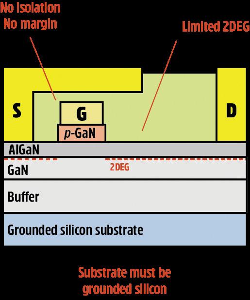
When dealing with noisy environments or high-power levels, a 1.6 V threshold may
not be enough. A negative gate drive of approximately -3 V will then likely be used, adding circuit complexity and additional dead-time loss. In fact, with a gate bias of -3 V, the reverse current flowing from source to drain must overcome the negative gate voltage, which causes additional undesired power loss. Notably, the negative drive’s negative impact on the dynamic or switching resistance of the device (which is the relevant resistance in the application) is not taken into account in E-mode device datasheets. It is a major topic of study and concern.1
The E-mode modifications indicated above come at a cost: the loss of gate isolation… and more.
Replacing the gate dielectric with p-type GaN makes the gate no longer isolated. Which, in turn, causes a significant gate current under positive bias, posing severe constraints to maximum gate voltage ratings. To reduce that significant gate current, yet another modification is made:
the gate contact is changed from an ohmic metal to a Schottky barrier [Figure 3B].
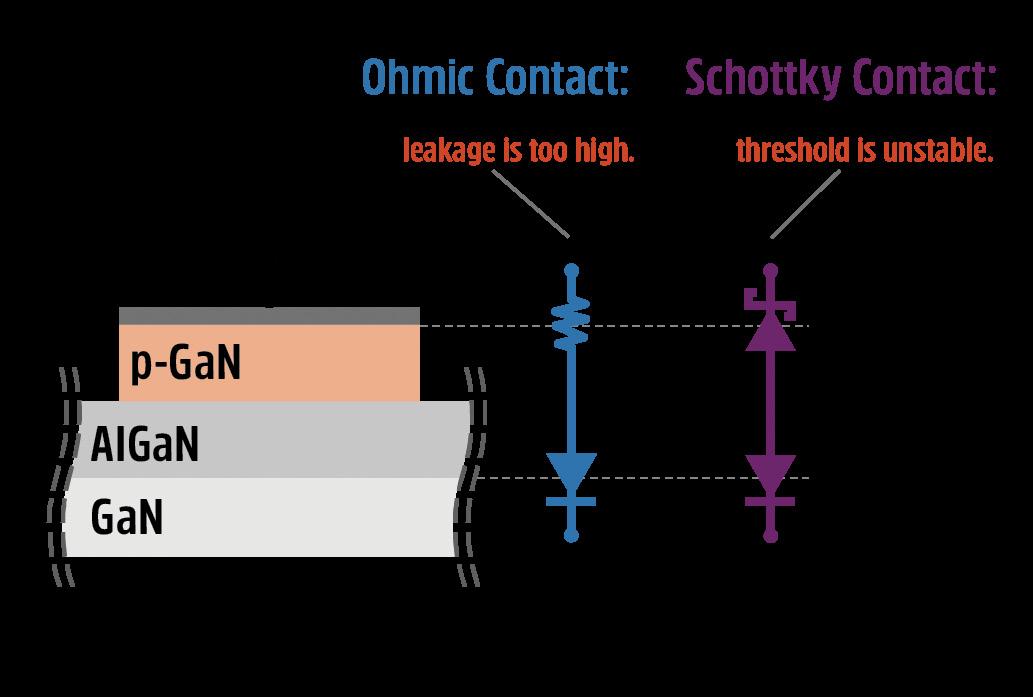
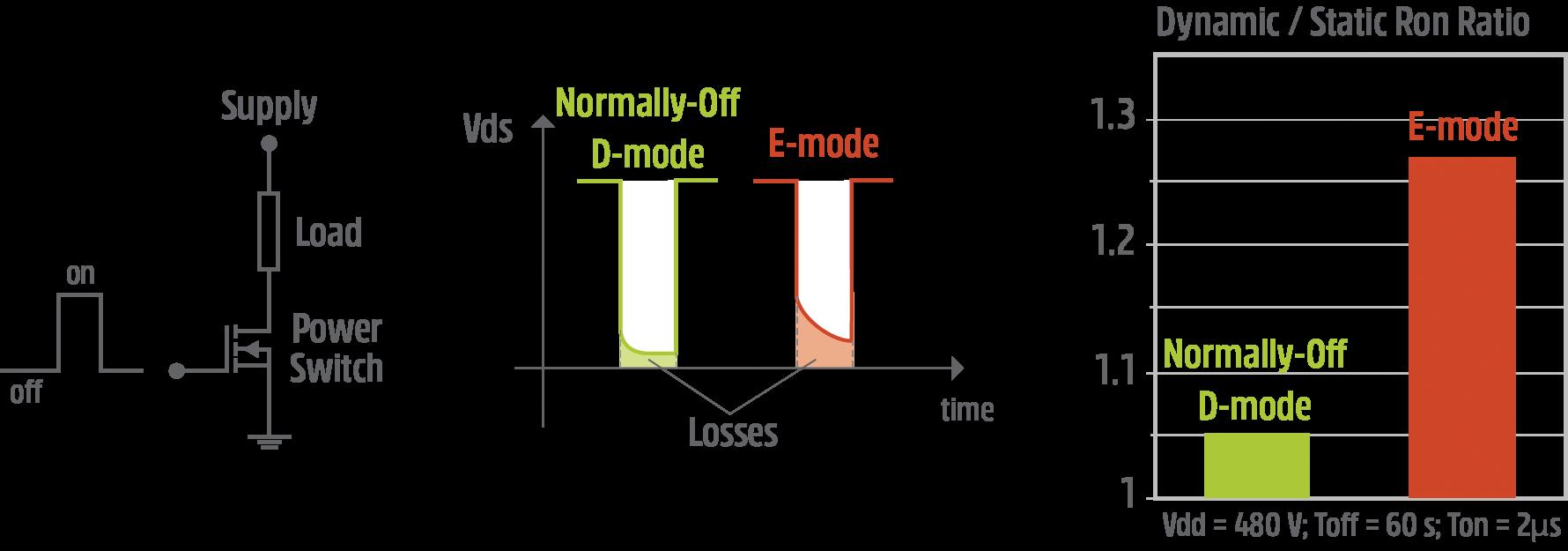
The Schottky barrier then introduces still another challenge as it now hinders the discharge of the gate-drain capacitance during turn-on transient. This, in turn, leads to a detrimental phenomenon referred to as “dynamic threshold” (reported by several research groups2, 3), which causes dynamic on-state resistance issues, as shown in Figure 4. At a voltage of 480 V, an E-mode device shows a dynamic RDS(on) increase of 27%, whereas its cascode counterpart shows only 5% resulting in less conduction losses. The E-mode data reported in Figure 4 is consistent with what’s shown in independent research studies.
Due to difficulty in discharging the capacitance, the E-mode device’s threshold voltage is now unstable during switching. This results in higher power losses versus its cascode counterpart. (Note: This is likely why E-mode manufacturers do not typically report dynamic RDS(on) ratings.) To mitigate this problem, one could theoretically overdrive the gate to reduce the RDS(on) of the device under the gate. However, this potential solution is up against a very tight voltage window as it must comply with a small gate maximum rating to prevent gate damage (max 7 V) [Figure 5].
Additionally, as temperature rises during normal device operations, the 2DEG mobility naturally decreases.
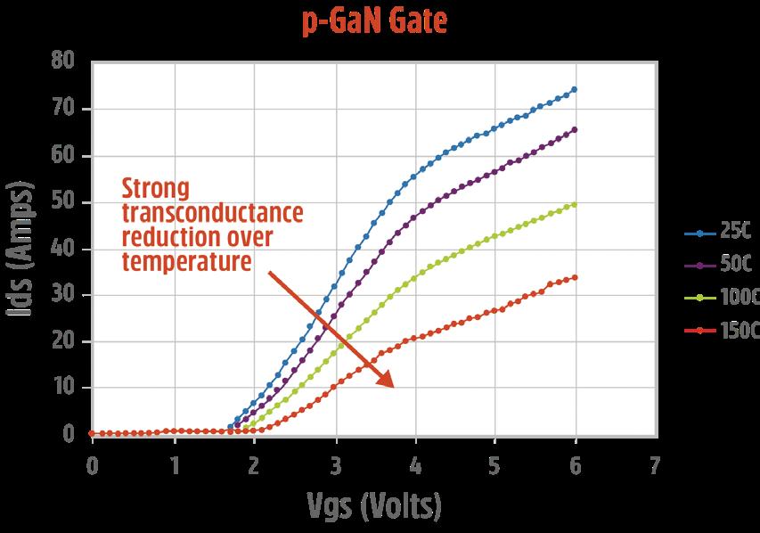
The reduction in 2DEG mobility over temperature also causes the p-GaN gate transconductance to drop [Figure 6], resulting in even slower transitions and still more switching losses5 versus that of cascode GaN. The decrease creates the perfect storm for low efficiency. To manage these issues, a p-GaN gate solution would need to start with a larger die, which still presents the problem of increased Miller capacitances, reducing overall efficiency and higher cost.
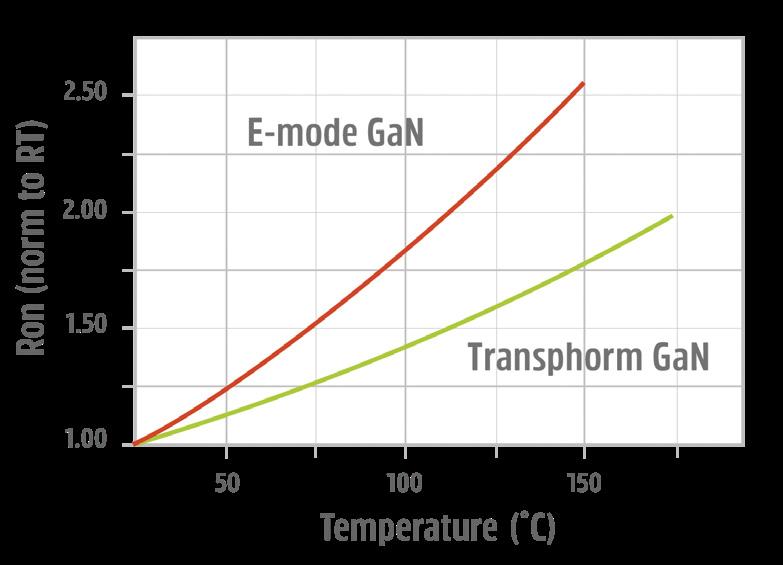
Per datasheet ratings, the E-mode device’s on-state resistance shows a higher temperature coefficient than cascode. In fact, it’s as high as 2.6x between 25°C and 150°C [Figure 7], yielding a rapid increase of conduction losses.
The E-mode design constraints continue with the susceptibility of threshold voltage drift due to trap injection into the buffer. E-mode’s silicon substrate must connect to the source terminal to mitigate buffer charging caused by electron injections from the source itself.
This modification restricts E-mode’s drain voltage maximum rating to 650 V. Given that higher voltages require thicker GaN buffers to support the substrate-to-source connection, E-mode devices are essentially left behind in the race to 1200 V as thicker GaN buffers require more sophisticated technology…which adds still more cost.
Transphorm approaches GaN power semiconductors differently. Again, its platform pairs the normally-on GaN HEMT with a highly reliable, highly performant, normally-off low-voltage Si MOSFET in a cascode configuration. This ensures the platform’s fail-safe normally-off operations
Figure 5. E-mode drive to fully enhance the channel is sensitive to damage due to only 1 V of headroom.
while retaining highest GaN performance and highest Si MOSFET gate reliability. Developing a cascode GaN platform was deliberate for various reasons; the most important two being that it works synergistically with nature and is backward compatible with today’s silicon technology.
by E-mode devices. For example, the cascode solution is unaffected by dynamic threshold issues since one drives a gateisolated low-voltage Si MOSFET. The threshold voltage is set by the Si MOSFET independent of the GaN HEMT.
The normally off cascode D-mode configuration also generates a second gift from nature in addition to the 2DEG: the SiO2/Si interface. This interface naturally isolates the device gate, offering the automotive-grade maximum gate rating of +/- 20 V with exceptional reliability and high drive margin. The threshold voltage is as high as 4 V, with no compromises on the 2DEG. The low-voltage Si MOSFET does not require negative bias or any special gate drivers. It is stable under all switching conditions, with no hidden power loss associated with dynamic
in
As stated earlier, it allows platform elements — particularly the 2DEG — to do what they do best. So, instead of limiting GaN’s advantages via E-mode (p-GaN gates), cascode embraces GaN’s potential. And the resulting cascode platform stands as a high-performing, highly robust GaN technology with industryleading reliability and versatility.
Cascode devices do not face the aforementioned challenges experienced
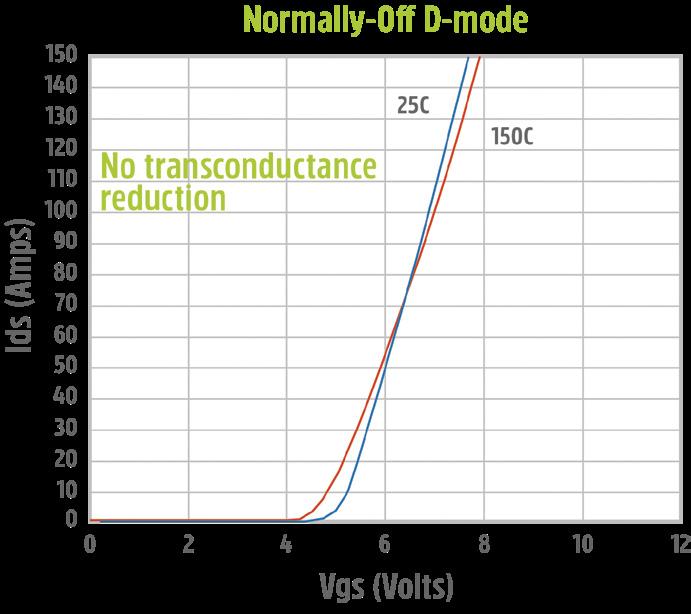
threshold issues. As can be seen in Figure 6B, the transconductance of cascode GaN devices is exceptionally high and doesn’t drop with temperature because it is set by the Si MOSFET and independent from the 2DEG mobility.
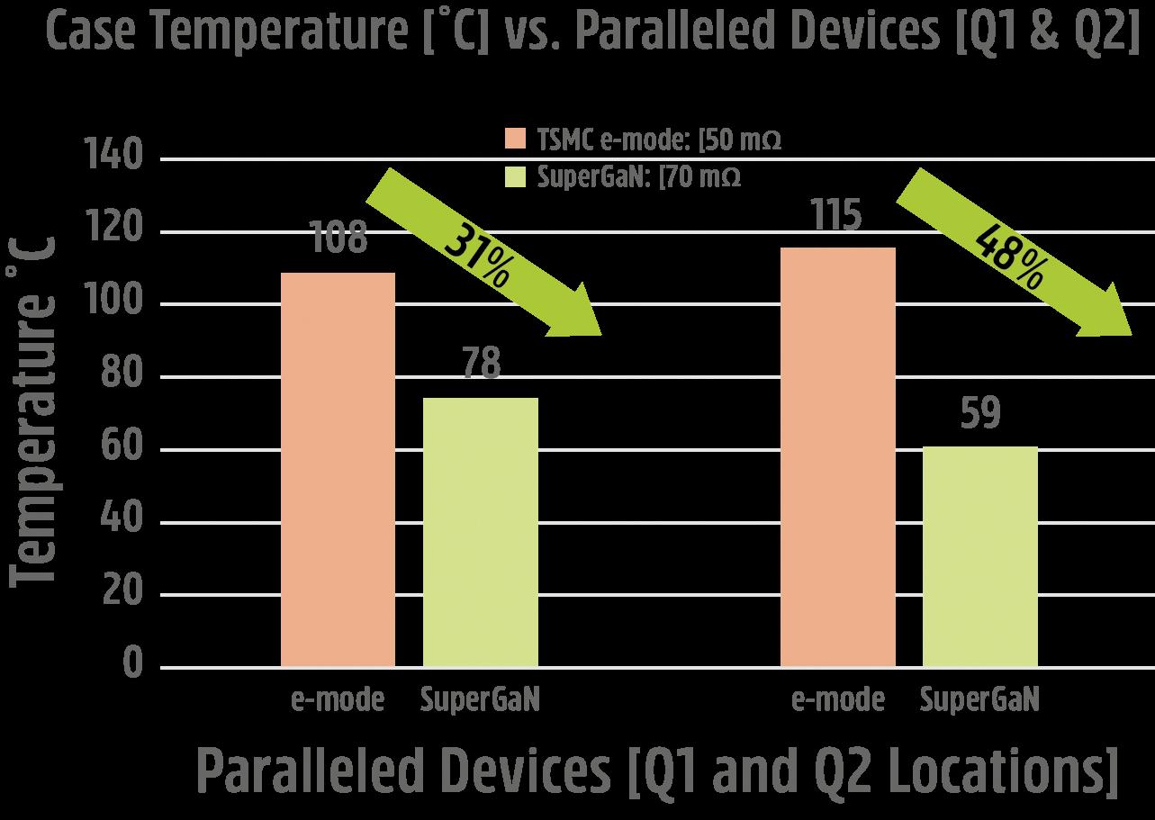
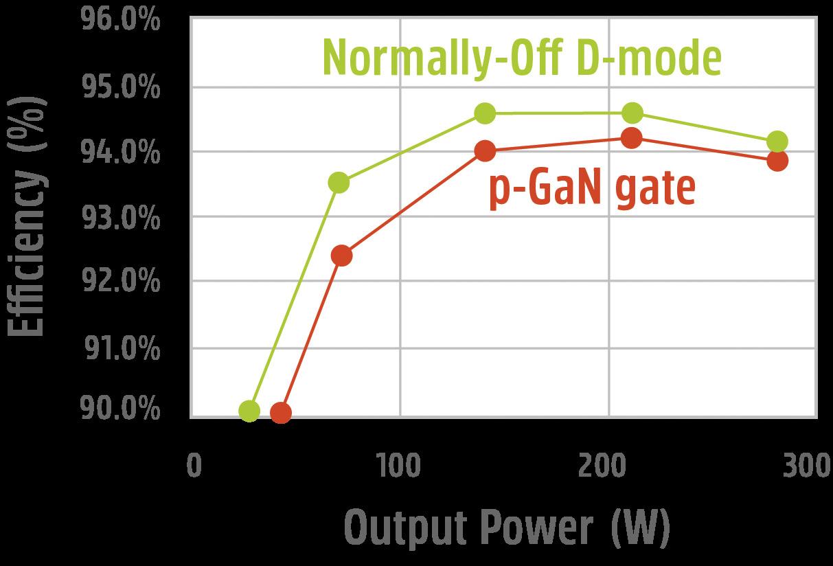
When Transphorm’s SuperGaN® cascode devices replaced the original E-mode GaN devices shipped in a commercially available power adapter, the SuperGaN FETs delivered higher efficiency and up to 50% lower case temperature despite having a smaller chip size and a 30% higher on-resistance rating [Figure 8].
The normally-off cascode platform fits elegantly in a broad range of standard packages such as through-holes, surface mounts, and multi-chip modules. These packages are considered high-performing and highly reliable in their own right, adding to the performance and reliability of the GaN platform itself.
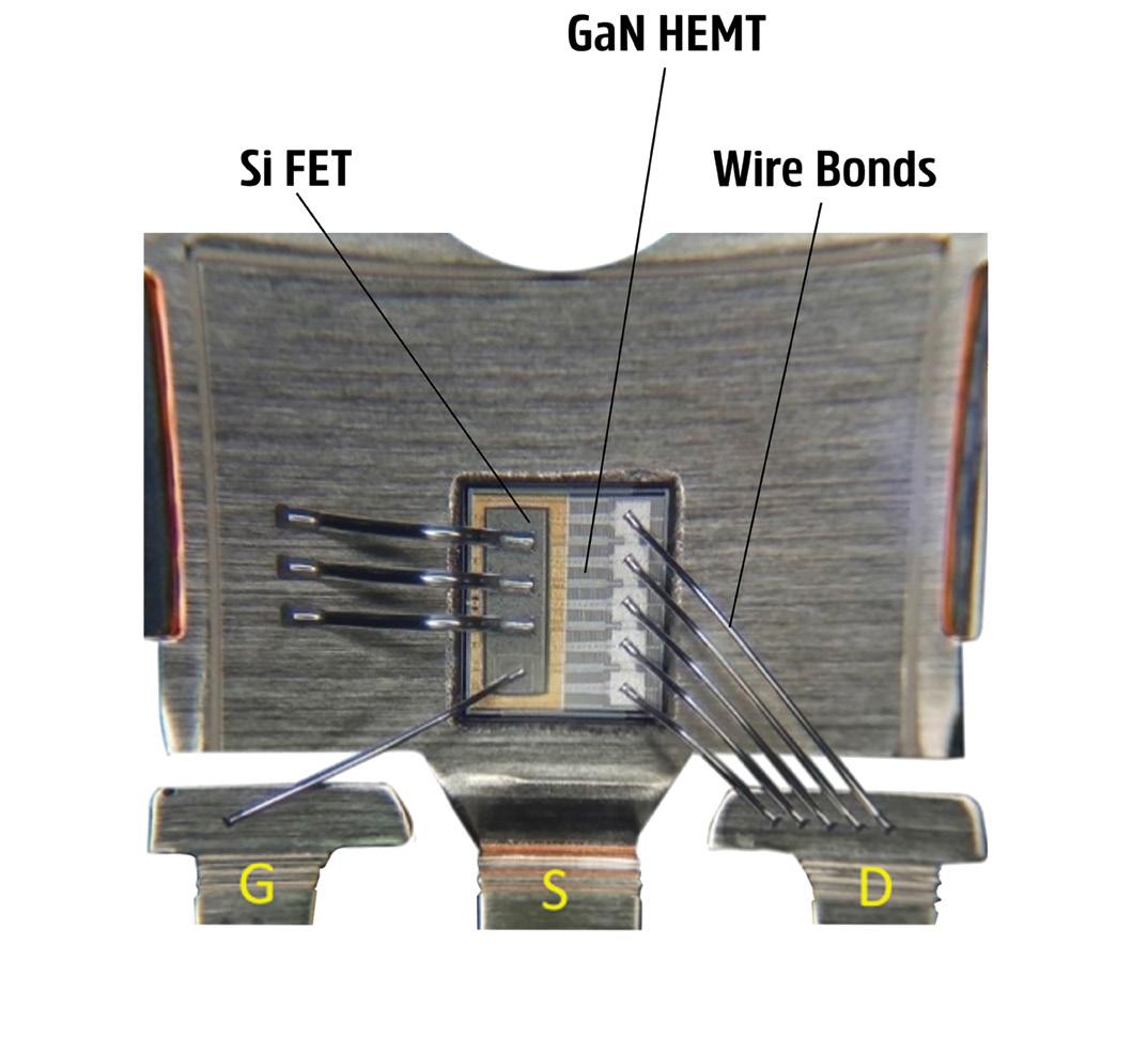
Modern assembly and packaging technologies minimize the parasitic inductances of Transphorm’s high-power cascode products. In fact, Transphorm’s SuperGaN normally-off cascode platform features a die-on-die technology with silicon-like wire bonding [Figure 9].
No additional wire-bonds or parasitic inductance are added, which allows for the desired connection scheme, including wire bond, copper clip, and Kelvin source.
The cascode configuration also lends itself beautifully to system-in-package integration, where the gate driver and controller are integrated seamlessly with
the D-mode HEMT and low-voltage Si MOSFET (monolithically or hybrid) — adding still another option to satisfy diverse end application requirements.
The cascode D-mode GaN HEMT does not need to connect the source to the substrate. A floating or insulating substrate enables a higher voltage rating (i.e., up to 1200 V7) and bidirectional switch implementation.
Interestingly, if one wants to develop a bidirectional switch using p-GaN gates, they will face yet another difficult decision: As both terminals alternate their polarity from ground to DC bus voltage, which terminal should the substrate connect to? It’s a question with no clear answer.
Yet another advantage: SCWT
As GaN transistors penetrate the motor drive market, short-circuit capability will be required. D-mode’s insulated gate voltage handling allows for very elegant design methods. Such methods are proven to tailor the short-circuit withstand time (SCWT) of Transphorm’s D-mode devices up to 5 microseconds,9 meeting the requirements of commercially available gate drivers. Transphorm achieves SCWT through its proprietary semiconductor process without adding additional masks or current sensing pins — making threeleaded packages still applicable. To date, E-mode does not seem fully prepared for this eventuality, with demonstrations being limited and sometimes misleading.
Conclusion
When considering the above-listed advantages and others, the normally-off
cascode D-mode platform generates a portfolio of GaN devices that optimize and magnify the inherent advantages of GaN as a semiconductor material — producing a truly revolutionary power conversion solution for next-generation power electronics.
References
"Dynamic Threshold Voltage in p-GaN Gate HEMT"
"Gate-Bias Induced RON Instability in p-GaN Power HEMTs"
“IG- and VGS-Dependent Dynamic RON Characterization of Commercial HighVoltage p-GaN Gate Power HEMTs”
"Assessment of the Switching
Characteristics of a commercial e-mode
Power GaN Device Using a Dual Pulse Test Set-up"
Recommended External Circuitry for Transphorm GaN FETs
"1200V GaN Switches on Sapphire Substrate"
Monolithic Bidirectional Power Transistors"
"Short-Circuit Capability with GaN HEMTs: Invited"
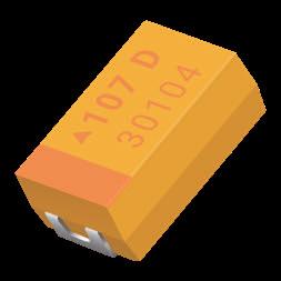
Tantalum Capacitor

•Audio Systems
•GPS
•Seat Controls
•Dashboard
Polymer Capacitor
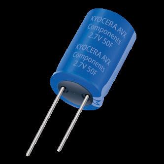
•Body Electronics
•Cabin Controls
•Infotainment
•Comfort
SuperCapacitor

•eLatch
•eCall
•Motor Stabilization
•eVideo / eCamera

carbide (SIC) MOSFETs and silicon (Si) IGBTs can both boost sustainability in green energy systems. Of course, they don’t compete across the board; there are uses where one or the other is clearly preferred. When comparing the two technologies, prioritizing performance characteristics like weight versus low cost often comes down to prioritizing performance characteristics. And both technologies continue to get better.
Si IGBTs are a mature technology advancing slower, while SiC MOSFETs are improving more rapidly. That can increase the complexity associated with choosing between the two. This article looks briefly at the changing tradeoffs between Si IGBTs and SiC MOSFETs, reviews some benefits of using Si IGBTs, challenges associated with using SiC MOSFETs in green energy applications, and closes by looking at advanced gate drives for SiC MOSFETs and advanced gate structures for Si IGBTs.
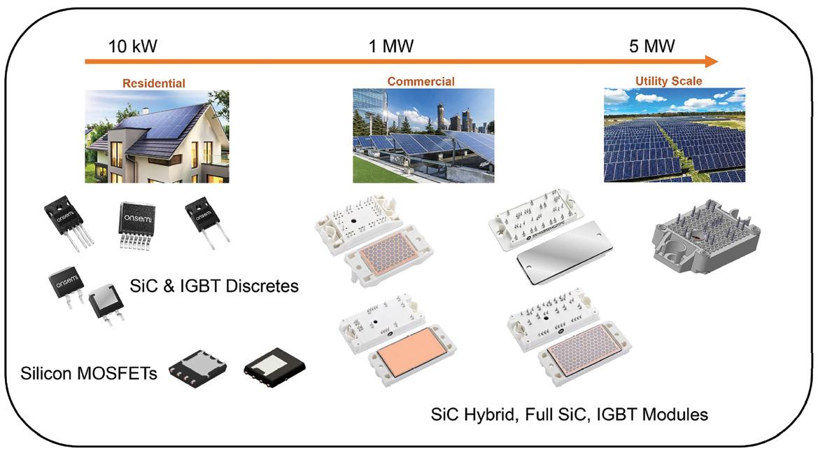
The choice is not simply Si IGBT versus SiC MOSFET; there is a continuum of options. For example, in the case of solar energy systems, low-power residential systems can choose between discrete Si and SiC MOSFETs and Si IGBTs. As the power level rises to commercial systems up to about 1 MW, the choices change to various modules, including Si IGBT modules, hybrid
modules with Si IGBTs and SiC diodes, and full SiC modules. At grid-scale power levels, high-voltage Si IGBT modules dominate (Figure 1).
As in most areas of technology, Si IGBTs are continually refined to better suit specific application needs. For example, in the case of commercial and grid-scale PV systems, bus voltages of 1.5 kV are being used in some designs to improve system efficiency. The highest voltage an IGBT must block shouldn’t exceed 80% of the VCES rating. Common IGBT module voltage ratings like 1.7 kV are limited to use with voltages up to about 1.3 kV and are not suited for use in most 1.5 kV PV systems, and 3.3 kV modules suffer from over-specification.
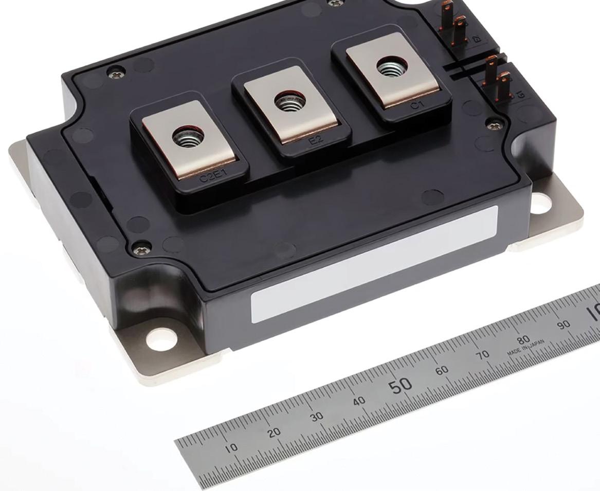
Using 1.7 kV or lower rated IGBT modules in 1.5 kV bus systems requires a more complex design, like a three-level neutral point clamped (NPC) topology that guarantees voltage sharing across modules. IGBT modules have been developed and rated for 2.0 kV to address the emergence of higher voltage buses. With derating, they can handle 1.6 kV and are suited for use with the new 1.5 kV buses. The 2.0 kV modules enable simpler topologies resulting in smaller and less expensive 1.5 kV rated PV inverters (Figure 2).
At the same time as IGBTs are being refined, SiC MOSFETs are evolving. In one case, a 2 kVA single-phase inverter was
Both technologies offer energy conversion efficiency, reduced losses, and greater system reliability for the grid — but there are tradeoffs.
Jeff ShepardImage: Adobe Stock
implemented using IGBTs and 1,200 V discrete SiC MOSFETs. The total losses (conduction + turn on + turn off) were about 41% lower for the SiC MOSFET design compared with the IGBT implementation, falling from 14.4 W using the IGBT to 5.9 W with the SiC MOSFET. Of course, the performance of SIC MOSFETs is improving at a more rapid rate compared with Si IGBTs, and the performance gap is widening accordingly.

IGBTs are suited for applications that benefit from medium-speed switching, need high voltages, low cost, and are not particularly sensitive to overall system size. It’s not just IGBTs versus SiC MOSFETs; in several types of inverter applications, like consumer white goods, IGBTs can be competitive with Si MOSFETs. Those applications are more sensitive to cost than maximum thermal performance. In other applications, thermal management can become a limitation for Si IGBTs. It’s not a simple ‘either or’ choice between power devices.
Si IGBTs and SiC MOSFETs are voltagedriven devices; an IGBT structure consists of a MOSFET driving a bipolar transistor. The bipolar nature of IGBTs enables them to carry high currents with low saturation voltages and low losses. SiC MOSFETs also have low conduction losses but have limited voltage ratings compared with Si IGBTs. For high-voltage and high-power applications, IGBTs are the preferred solution. On the other hand, SiC MOSFETs are more thermally rugged, making them more suited for hightemperature environments.
In medium voltage applications, where the choice is between Si IGBTs and SiC MOSFETs, the higher losses associated with IGBTs can become a significant consideration. Thermal management raises the cost of using IGBTs, and their slower switching speeds can increase the cost of passive components like capacitors and inductors. But even then, the
overall system cost is not a simple equation. Using SiC MOSFETs in green energy systems Is not simply a matter of replacing Si IGBTs with SiC MOSFETs. Using SiC MOSFETs requires a different design approach, resulting in a learning curve for designers unfamiliar with the technology, increasing the design risk and potentially delaying time to market. Those are some factors hindering the adoption of SIC MOSFETs, even in applications that may benefit from the performance improvements they offer. For example, printed circuit board (PCB) design is an essential factor in power converters, and SiC MOSFETs have different
also important and different compared with IGBTs. Faster switching is again the culprit. A tight gate drive PCB layout is needed to minimize undesired characteristics like oscillations, overshoots, EMI, and other factors. Low inductance drive loops are essential, and parasitic capacitances must be minimized.
Gate drive optimization is vital to maximizing the performance of Si IGBT and SiC MOSFETs. In the case of SiC MOSFETs, minimizing
PCB needs compared to Si IGBTs. Some examples include:
• Faster switching speeds produce faster di/dt and dv/dt slew rates. That means designers must consider factors like false turn-on, parasitic resonances, cross talk, and increased electromagnetic interference (EMI).
• PCBs for SiC MOSFET power converters can be smaller, but they still require the same creepage and clearance distances required for all power converters. It’s not just the devices; their smaller heatsinks can also impact creepage and clearance performance.
• Efficient driving for SiC MOSFETs is
Figure 1. There’s a continuum of green energy applications for Si and SiC MOSFETs and Si IGBTs (Image: onsemi)
switching and conduction losses during turnon and turn-off is necessary. With conventional gate drivers, there can be a tradeoff between faster switching speed and increased transient overshoot. An adaptive drive scheme has recently been advanced for SiC MOSFETs that addresses that tradeoff.
The new approach varies the gate drive current and enables overshoot management (Figure 3). It has been optimized for use in EV battery packs. For battery packs charged from 80% to 100%, a low gate drive strength can be used to optimize overshoot while maintaining efficient SiC MOSFET operation. When supporting packs between 80% and 20% of full charge, battery chargers
can benefit from a high-strength gate drive to reduce switching losses. By optimizing the gate drive current between 5 and 20 A, a 2% overall efficiency increase can be realized for EV battery chargers.

IGBTs have been highly refined over many years, making it increasingly challenging to realize significant performance improvements. For example, reducing overall power losses is difficult since, in a conventional IGBT design, reducing conduction losses generally leads to increased switching losses.
Much of the challenge is from the tail current attributable to minority carriers when an IGBT turns off. As the device
been demonstrated that turning the gates on in that order results in large electron and hole flows, turning the device on faster with lower turn-on losses. When turning the device off, CGs remains off, and CGp is turned off before MG. When MG turns off, the electrons and holes are quickly removed, reducing turn-off losses. The proposed three-level gate drive technique with a prototype 1.2 kV TG-IGBT resulted in 66% lower turn-on and 35% lower turn-off losses than a conventional device structure.
SiC MOSFETs continue to improve and are increasingly encroaching on applications dominated by Si IGBTs. At the same time, IGBT performance is improving, but at a

2.0kV IGBT Module for Industrial Use, Mitsubishi Electric
Designing with Silicon Carbide for High Efficiency Renewable Energy Systems, Wolfspeed
Getting the most out of IGBTs is about knowing When, Where and How to Use Them, onsemi
How to maximize SiC traction inverter efficiency with real-time variable gate drive strength, Texas Instruments
IGBT & SiC Gate Driver Fundamentals, Texas Instruments
turns off, the depletion region expands, increasing the collector-emitter voltage, and the minority carriers become part of the internal recombination current — the tail current that appears during the later stages of turn-off and is a significant contributor to switching losses. To reduce switching losses, IGBTs are designed with an “optimal” mix of minority carrier lifetime and the number of holes injected from the collector. Both these approaches increase on-state resistance. A third option has been recently proposed.
To improve IGBT switching performance and maintain low on-state resistance, it’s been proposed to replace the single gate with three gates, a main gate (MG), and primary and secondary control gates, CGp and CGs, respectively (Figure 3). When turning the triple gate IGBT (TG-IGBT) on, MG and CGp are turned on simultaneously, and CGs is delayed and is on for a brief period. It’s
slower pace. Additionally, new gate drive approaches are being developed for both types of devices. The choice between Si IGBTs and SiC MOSFETs will remain a complex and crucial decision for the foreseeable future.
Three-level Gate Drive Technique for Enhancing Switching Loss Reduction in Triple-Gate IGBTs, 2022 IEEE 34th International Symposium on Power
Semiconductor Devices and ICs (ISPSD) What are the merits of using SiC MOSFETs?, Toshiba

INmany critical applications running from the AC mains, an uninterruptible power supply (UPS) is used to provide temporary power in the event of a complete outage and to ensure that the supply voltage remains within specification, which is particularly important where the load is susceptible to dips or fluctuations in the mains voltage.
There are two types of UPS: online and offline. Online is the preferred approach as it is able to switch seamlessly from grid power to battery power when needed. This type of UPS receives its input power from the grid and supplies its output to the load
— often a server in a data center or critical equipment on a factory production line.
The first step within a UPS is to convert the incoming AC voltage into DC using an AC-DC converter. This voltage is then fed into the UPS’s internal battery, ensuring that it is constantly charged so that the maximum runtime is available in the case of a power outage. This battery voltage is then converted back to AC using a DC-AC converter to provide a voltage at the same level as the grid to power the load. As the battery is always connected or online, this type of UPS is called an online UPS.
In the case of a power outage, the battery supplies the inverter, and the output AC voltage remains present while the charge remains in the battery, allowing the load to continue to run
The key to success lies in the adoption of technologies like discrete SiC and modern topologies to craft small, yet highly efficient single online UPS designs.
Hunter Freberg, onsemiFigure 1. Schematic diagram of an offline UPS and an online UPS.
and/or be shut down in an orderly manner. It also eliminates spikes on the grid, and voltage/frequency fluctuations, ensuring that the voltage to the load remains within specification.
The main advantage of an online UPS is the fast reaction time, as the battery can be quickly connected to the output. This advantage, however, comes at the expense of double conversion from AC to DC and back to AC again. As efficiency can never be 100%, an online UPS wastes slightly more energy than its offline cousin. Though this is a minor issue, so an online UPS is by far the more prevalent technology.
Depending upon the design and the needs of the load, a UPS can be single or three-phase. In a three-phase design, a topology known as a Vienna rectifier is often used for the input (AC-DC) stage that feeds DC to the battery. After an input filter, each phase of the incoming voltage is passed through an inductor before the Vienna rectifier.
The output of the rectifier is a DC bus of around 800V , based on typical global three-phase voltage levels; this provides approximately 400 V across each of the DC bus capacitors.
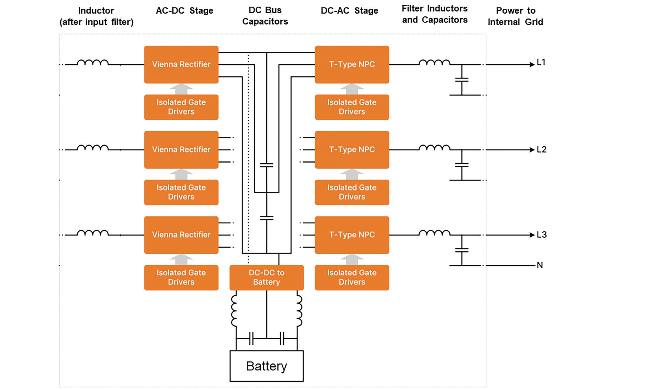
Not only does the energy stored in the DC bus capacitors charge the battery, but it also drives the output stage, which is often a neutral-point-clamped (NPC) T-type converter. When the grid voltage is present, the capacitor energy is replenished directly from the grid voltage. In the event of a grid failure, this energy will come from the battery — ensuring that the T-type NPC can continue to deliver AC power to the load.
A typical three-phase Vienna rectifier consists of twelve power components, six diodes, and six IGBTs. Often silicon carbide (SiC) is used for its performance advantages, with the diodes and IGBTs having voltage ratings of 1200 V and 650 V, respectively. When there is IGBT optimization for low VCE, and a choice of medium speed or high speed, the medium speed options are often preferred, as both switching and conduction losses are important in this topology for the central switch. onsemi offers a number of power modules based on these topologies to simplify development and improve performance over discrete designs.
A three-phase T-type NPC also uses twelve components, although in this case, they are all IGBTs. The back-to-back devices are rated at 650 V. The IGBTs connected to
DC+ and DC- are 1200 V IGBTs. There are a total of twelve components.
Using silicon carbide to reduce losses
As noted, online UPS has a double conversion which allows the online topology to function but introduces additional losses. The issue is somewhat compounded as the losses generate heat which can require a more powerful HVAC system to maintain room temperature. This will incur capital costs in buying the HVAC system, operating costs for the extra space for running the bigger HVAC, and for the cost of energy lost in the UPS.
If the UPS size can be reduced, then the data center operator benefits as this space can be used for revenue-generating servers. Reducing losses will also reduce operating costs and generally lead to a smaller solution, as power density can increase with lower losses. As wide-bandgap (WBG) materials such as silicon carbide (SiC) generally have better performance and lower losses, adopting this technology will enhance the UPS efficiency. They also offer better efficiency at light loads as the series resistance is lower and there is no anti-parallel diode, as there is in IGBTs, nor a fixed voltage drop.
One of the challenges in sizing IT
systems, including UPS, for use in IT systems is the dynamic nature of the load. A computer uses significantly less energy when browsing the web or writing a document than it does when performing machine learning or running a detailed simulation. As SiC offers enhanced efficiency, whatever the load levels, this dynamic load is a further reason why SiC is rapidly becoming the preferred technology.
Due, in part, to the lower levels of gate charge (Qg), SiC devices are able to maintain efficiency while switching at higher frequencies. One effect of this is to reduce the size of the reactive components, which can contribute significantly to a reduction in the overall size of the UPS.
A further benefit of using SiC is the ability to move from a Vienna rectifier / T-type NPC to ‘six-switch’ converters on the input and output (AC-DC and DC-AC) stages, meaning that the topology can be replicated, saving design time. The six-switch topology consists of three half-bridges, reducing by half the number of semiconductors in the design, space and cost saving the smaller magnetics are retained.
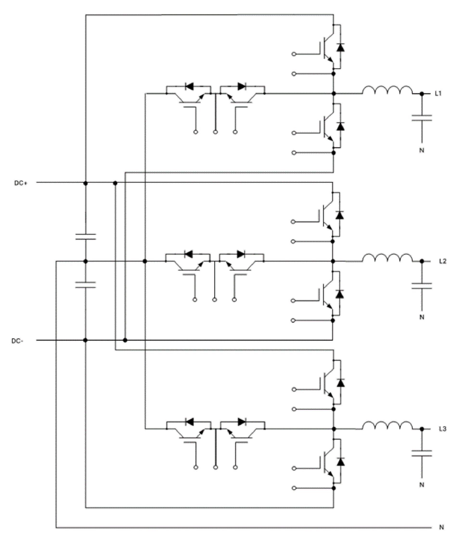

In this example, due to the grid voltages, the EliteSiC MOSFETs will be 1200 V rated.
onsemi has a number of SiC MOSFETs that are suited for use in six switch converters. One example is the high-speed M3S NTH4L022N120M3S or the more recent NTH4L040N120M3S. For further performance benefits, one may also consider using modules in their design, such as onsemi’s latest NXH003P120M3F2 1200 V half-bridge modules based on M3S SiC technology.
The AC-DC front end can be used bidirectionally, allowing feedback of reactive power to improve the power factor, which reduces apparent power and, therefore, operating costs.
Moving from a silicon solution to SiC requires a change to the drivers used for the switches. The selected SiC MOSFETs require dual 5kV isolation and fast operation (dv/dt, propagation delays) to allow the SiC MOSFETs to operate at optimum performance.
A suitable driver is onsemi’s NCP51561 — its dv/dt capability is over 210V/ns and the propagation delay is just 39ns, matched to 5ns between channels. The device also features an external dead time control and an enable pin, which enhance system reliability.
In summary, a single online UPS is essential to the continuous operation of servers and critical machinery. In order
to produce a winning design, engineers need to be able to develop small and efficient designs. The best way to do this is to adopt discrete SiC technologies and modern topologies, such as six-switch conversion, and use these in conjunction with high-performance SiC drivers.
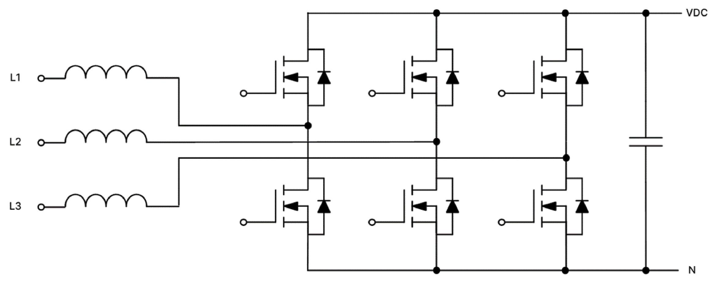
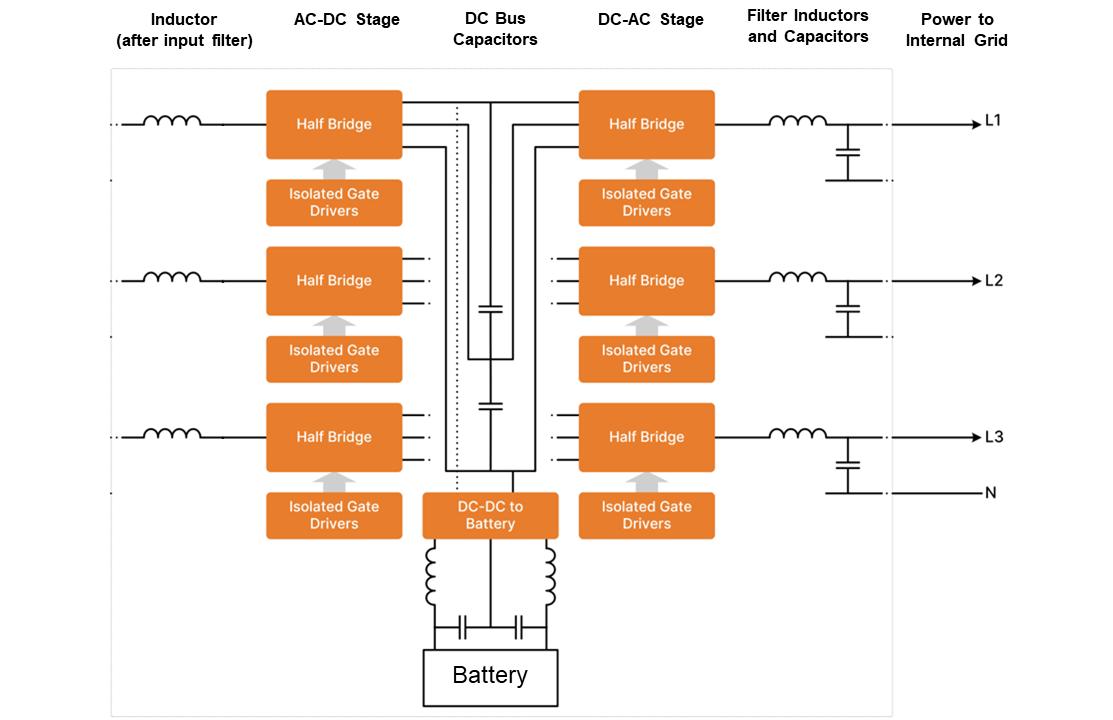







SEQUOIA SERIES
• Four-Quadrant Regenerative Grid Simulator with Add-On Electronic Load Option
FEATURES AND CAPABILITIES

TAHOE SERIES
• Two-Quadrant High Power AC/DC Source with Advanced Power Analyzer
• Dual Voltage ranges that support over voltage testing on 480V based systems

• 500uS time resolution for Transients
• Virtual Panels control software included
• Trigger In & Out to permit extensive coordination with external systems
• Intuitive 5” color display for ease of navigation
• Auto-paralleling for maximum flexibility with multi-chassis configurations
TDK’s Aluminum Electrolytic Capacitors offer a wide range of solutions for power and energy applications. The product portfolio features superior ripple current capabilities, compact design, long service life, and long-term reliability. The complete selection includes screw terminals, snap-in and multi-pin series with many special characteristics and benefits.
Applications
• Photovoltaic (PV) systems

• Wind power
• Medical applications
• Power supplies Learn