8 minute read
The try-before-you-buy route to energy efficient power design


Xuning Zhang, Levi Gant • Littelfuse, Inc.
Evaluation platforms help pick SiC components in power conversion circuits.
The quest for greener energy production and consumption has put a premium on high-efficiency power circuitry. In that regard, many modern power supplies and converters operate at much higher voltages that allow use of lower currents to minimize I 2 R losses. Silicon carbide (SiC) MOSFETs and diodes are important elements of these new high-power, high-voltage power conversion circuits.
SiC MOSFETs provide low on-resistance and can switch back and forth between on and off states rapidly. Consequently, they dissipate much less power than insulated gate bipolar transistors (IGBTs) which have slower turn-off speeds and higher turn-off switching power loss. In addition, silicon carbide’s wide bandgap enables SiC devices to operate at high voltages. In contrast, silicon-based MOSFETS can’t realize both high blocking voltages and low on-resistances. As a result, SiC devices are becoming integral in high-power applications.
Because of the high power levels SiC devices deal with, designers must evaluate both the SiC devices themselves and their gate driver circuits. SiC technology is still relatively new, and device performance under a wide range of conditions is not fully characterized.
An evaluation platform will enable design engineers to evaluate SiC MOSFETS, SiC Schottky diodes, and gate driver circuits under continuous operation in converter circuit applications. The evaluation platform will aid in accelerating design cycles for successful, SiCbased power converter design and assist in speeding the time-tomarket for the end product.

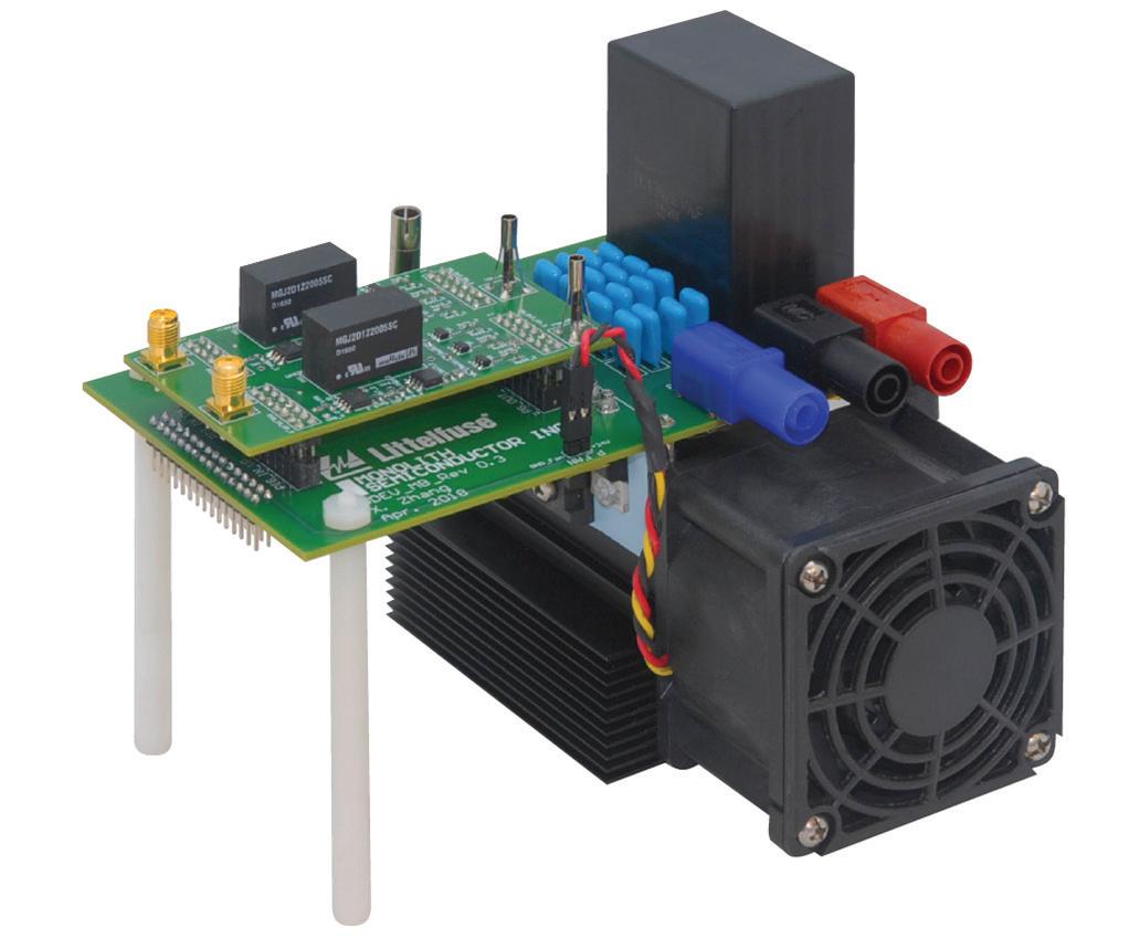
The gate drive evaluation platform includes the motherboard, two plug-in gate driver modules, and the heatsink and fan to support up to 5 kW of output power.
DESIGN CHALLENGES FOR POWER CONVERSION CIRCUITS
To maximize power output and efficiency of power conversion circuits, designers must ensure that:
• The power devices can perform at rated power and current and deliver enough power to the load
• The circuit minimizes internal power loss for maximum efficiency
• The design incorporates protection circuitry for the SiC power devices
• Printed circuit board (PCB) layout minimizes parasitic inductances and capacitances
• EMI emissions are within allowable limits
• The design uses a minimum of passive components to help keep down cost, size, and weight
• The gate driver helps realize the above goals and assists in maintaining thermal performance within specified temperature ratings.
A gate drive evaluation platform helps designers address all these challenges. The platform can operate at high power levels continuously to characterize the performance of the selected SiC MOSFETS and diodes. The platform also enables the comparison of different gate drivers under multiple test conditions. Gate drivers can be evaluated for thermal performance, EMI immunity, and the capability to drive the power components so they operate at high efficiency. Finally, the platform allows analysis of the design for efficiency improvements, electromagnetic interference (EMI) emissions, cost, size, and weight.
The gate drive evaluation platform is essentially a power stage reference design consisting of a motherboard with two SiC MOSFET-SiC Schottky diode pairs in a half-bridge configuration. The half-bridge circuit can output a maximum of 5 kW with an 800-Vdc bus voltage. The motherboard can accommodate two separate gate driver module boards, one for each switch position. Thus, different gate driver integrated circuits and gate driver designs can quickly and easily mount on the motherboard to evaluate gate driver performance and how the driver impacts output power.
The third major element of the gate drive evaluation platform is the thermal management, a heatsink and a fan which cools the MOSFET-diode pairs. The heatsinkfan subsystem enables the power circuit to deliver up to 5 kW continuously with the MOSFET-diode pairs switching at frequencies up to 200 kHz.
The gate drive evaluation platform’s printed circuit board layout minimizes both loop inductance and coupling between the power circuit and the gate circuit. The two gate driver circuits allow independent evaluation of both the top and bottom gate-driving qualities.
The selection of SiC MOSFETs and diodes and the selection of the gate driver are the most important decisions for the power conversion design. The MOSFET must have the voltage, current, and power specifications to meet the converter requirements. The gate driver has more sophisticated requirements. It should have a wide voltage range and enough output current to drive the power MOSFET.
Recommended drive voltages are 15 to 20 V to switch the MOSFET to its onstate and a voltage of 0 to -5 V to switch the MOSFET to the off-state. The peak output current for the gate drive can range from 1 to 15 A depending on the MOSFET power handling capacity. The driver needs to provide a high pulse current to reduce MOSFET switching loss during switching transients. In addition, high continuous current with small external gate resistances reduces driver temperature during high frequency switching of the SiC MOSFET.
The high dv/dt caused by fast SiC MOSFET switching makes high commonmode currents flow through the gate driver and the rest of the power conversion circuit. High common-mode currents can affect the voltage reference node in the control circuit, causing incorrect operation. The magnitude of the common-mode current is determined by the MOSFET dv/dt and the impedance in the common-mode current path. Consequently, the gate driver IC and its power supply both need a high isolation impedance to reduce common-mode current. The isolation capacitance of the gate driver should be less than 1 pF. The isolation capacitance of the power supply should be under 10 pF.
Traditionally, optocouplers would provide the isolation. Newer IC technology can employ inductive or capacitive isolation. The new methods are known as digital isolator techniques. The optocoupler and the digital isolator have both advantages and disadvantages. The optocoupler sources current which makes its input less susceptible to EMI. However, optocouplers can’t handle data transmission rates as high as those of digital isolators and bring longer pulse-width distortion times. Pulse-width distortion time refers to signal delay time through the driver IC. In a half-bridge power conversion topology, excessive delay can create waveform distortion and low frequency noise.
Optocoupler performance varies with the drive voltage, temperature, and device age. Digital isolator-based drivers have more stable parameters over temperature. Because digital isolators operate with a voltage input, they can be more susceptible to EMI. But all in all, the digital isolator’s more stable operating parameters makes it a better choice than optocouplers in gate drivers for power conversion circuits using SiC MOSFETs.
With high-power circuits, protection mechanisms are necessary to prevent device thermal runaway and device and circuit damage from fault conditions. Gate driver ICs that incorporate protection circuitry are highly recommended. Gate drive ICs should have de-saturation (de-sat) protection, soft turn-off during a fault condition, a Miller clamp circuit, and under-voltage lock out (UVLO).
De-sat protection circuitry turns off a MOSFET in the event of a load short-circuit. Soft turn-off avoids a large transient voltage overshoot and turns off the MOSFET during a shoot-through failure (where both MOSFETs are momentarily on simultaneously). A Miller clamp circuit prevents the shoot-through condition by draining current from the parasitic drain-gate capacitance to avoid a transient rise in the gate voltage. The clamp circuit keeps the MOSFET from turning-on when it should be in the off-state. If voltage supply for either the gate driver input or for the isolated output circuit gets too low, the UVLO circuit turns off the gate drive to protect the MOSFETs from improper switch timing. These protection circuits ensure a more robust and safe power conversion circuit.

Waveforms resulting from test conditions: input voltage = 800 V, output voltage = 400 V, switching frequency = 100 kHz, and output power = 2.5 kW.
PCB board layout has a major impact on the performance of dynamic circuits such as high-efficiency power conversion circuits. Parasitic capacitance and inductance from PCB traces and ground planes add to the parasitic capacitance and inductance in the circuit. Parasitic components in the gate drive loop degrade MOSFET switching performance. Gate-source capacitance forces a higher driving current from the gate driver IC. Stray inductance boosts gate-source voltage overshoot and leads to ringing during MOSFET switching.
To minimize the stray capacitance and inductance, keep the gate path as short as possible by placing the gate driver, the gate resistor, and the decoupling capacitor close to the MOSFET gate. Minimize loop inductance by routing the gate return path directly below the gate supply trace. Maximize the distance between the MOSFET gate traces and the drain traces to reduce the size of the gate-drain capacitance. This practice cuts the current entering the gate which reduces the Miller effect.
Additionally, ground planes under power conversion circuits add capacitive coupling; avoid use of ground planes for MOSFET switching-based power conversion circuits. All these PCB layout recommendations have been implemented in the gate drive evaluation platform to avoid design, layout, and test of a custom test board.
The gate drive evaluation platform can easily compare switching loss and switching transients using different gate drive ICs. Consider the case of evaluating gate drivers for a buck converter operating under continuous switching conditions. The buck converter operates at 100 kHz and will output 2.5 kW.
The drive capabilities of driver ICs and the external gate resistances used will influence the SiC MOSFET switching transients and the overall switching losses. In this test, the first gate driver has a drive current rating of 14 A and the second has a drive current rating of 2 A. Each gate driver was tested with a 10-Ω and a 1-Ω gate resistor.
The 10-Ω gate resistor eliminates differences in the performance of the gate drivers. The 10-Ω gate resistor does slow MOSFET transient switching speed which increases switching loss. The differences between the high-output-current driver and the low-output-current driver are more significant. The MOSFETs switch faster when the high output current driver is used with a lower gate resistance. The lower gate resistance does exhibit more ringing during a switch transition than the higher gate resistance. The designer must find the optimum combination of gate driver, gate resistance, and MOSFET to minimize switching loss.
The gate drive evaluation platform can help evaluate driver IC thermal performance thanks to the heatsink and fan that enable the MOSFETs to operate in a continuous switching output state. The platform can also be used to test driver protection functions.
In a nutshell, gate drive evaluation platforms are a tool that facilitates the evaluation of SiC devices and the gate drivers. With gate drive modules plugged into the motherboard, designers can easily compare efficiency and thermal performance with different gate driver ICs. Designers can use the PCB layout techniques on the evaluation platform and the component recommendations to overcome the design challenges of SiC devices to develop efficient, thermallycontrolled, and protected power conversion circuits. As a result, the evaluation platform enables faster design of efficient power conversion circuits and speeds product time-to-market.
REFERENCES: Littelfuse application note on the gate drive evaluation platform, littelfuse.com/gdevappnote


