






PITTCON IS A CATALYST OF SCIENTIFIC ADVANCEMENT for you, your research, your career, your organization, and together, our world. Our aim is to provide you with unparalleled access to the latest advances in laboratory science, to the instrumentation enhancing your work, and to an international assembly of scientists experimenting, discovering, and innovating throughout the foremost areas of focus.
LEADING IN THE LAB STARTS AT PITTCON.ORG
Philadelphia, PA, USA | March 18-22, 2023
EDITORIAL
VP, Editorial Director Paul J. Heney pheney@wtwhmedia.com @wtwh_paulheney
Associate Editor Heather Hall hhall@wtwhmedia.com
Senior Editor Rachael Pasini rpasini@wtwhmedia.com
Senior Contributing Editor Leslie Langnau llangnau@wtwhmedia.com
Executive Editor Leland Teschler lteschler@wtwhmedia.com @dw_leeteschler
Executive Editor Lisa Eitel leitel@wtwhmedia.com @dw_lisaeitel
Senior Editor Aimee Kalnoskas akalnoskas@wtwhmedia.com @EEWorld_Aimee
Senior Editor Miles Budimir mbudimir@wtwhmedia.com @dw_motion
Associate Editor Mike Santora msantora@wtwhmedia.com @dw_mikesantora
DIGITAL MARKETING

VP, Digital Marketing Virginia Goulding vgoulding@wtwhmedia.com @wtwh_virginia
Digital Marketing Coordinator Emily Gillespie egillespie@wtwhmedia.com @wtwh_emily
Digital Production/ Marketing Designer Samantha King sking@wtwhmedia.com
Marketing Graphic Designer Hannah Bragg hbragg@wtwhmedia.com
Webinar Manager Matt Boblett mboblett@wtwhmedia.com
Webinar Coordinator Halle Kirsh hkirsh@wtwhmedia.com
Webinar Coordinator Kim Dorsey kdorsey@wtwhmedia.com
FINANCE Controller Brian Korsberg bkorsberg@wtwhmedia.com
Accounts Receivable Specialist Jamila Milton jmilton@wtwhmedia.com
VIDEO SERVICES
Video Manager Bradley Voyten bvoyten@wtwhmedia.com @bv10wtwh


Videographer Garrett McCa erty gmccafferty@wtwhmedia.com
Videographer Kara Singleton ksingleton@wtwhmedia.com

VP, Creative Services Mark Rook mrook@wtwhmedia.com @wtwh_graphics
Art Director Matthew Claney mclaney@wtwhmedia.com @wtwh_designer
Senior Graphic Designer Allison Washko awashko@wtwhmedia.com @wtwh_allison
Graphic Designer Mariel Evans mevans@wtwhmedia.com @wtwh_mariel
Director, Audience Development Bruce Sprague bsprague@wtwhmedia.com
Web Development Manager B. David Miyares dmiyares@wtwhmedia.com @wtwh_webdave
Senior Digital Media Manager Patrick Curran pcurran@wtwhmedia.com @wtwhseopatrick
Front End Developer Melissa Annand mannand@wtwhmedia.com
Software Engineer David Bozentka dbozentka@wtwhmedia.com
Digital Production Manager Reggie Hall rhall@wtwhmedia.com
Digital Production Specialist Nicole Lender nlender@wtwhmedia.com
Digital Production Specialist Elise Ondak eondak@wtwhmedia.com
Digital Production Specialist Nicole Johnson njohnson@wtwhmedia.com
VP, Strategic Initiatives Jay Hopper jhopper@wtwhmedia.com
EVENTS

Events Manager Jen Osborne jkolasky@wtwhmedia.com @wtwh_jen
Event Marketing Specialist Olivia Zemanek ozemanek@wtwhmedia.com
Event Marketing Coordinator Alexis Ferenczy ozemanek@wtwhmedia.com
Customer Service Manager Stephanie Hulett shulett@wtwhmedia.com
Customer Service Representative Tracy Powers tpowers@wtwhmedia.com
Customer Service Representative JoAnn Martin jmartin@wtwhmedia.com
Customer Service Representative Renee Massey-Linston renee@wtwhmedia.com
Customer Service Representative Trinidy Longgood tlonggood@wtwhmedia.com
WTWH Media, LLC
1111 Superior Ave., Suite 2600 Cleveland, OH 44114
Ph: 888.543.2447

FAX: 888.543.2447
R&D
relevant to industry issues. Letters to the editor and by-lined articles express the views of the author and not necessarily of the publisher or the publication. Every effort is made to provide accurate information; however, publisher assumes no responsibility for accuracy of submitted advertising and editorial information. Non-commissioned articles and news releases cannot be acknowledged. Unsolicited materials cannot be returned nor will this organization assume responsibility for their care.
R&D WORLD does not endorse any products, programs or services of advertisers or editorial contributors. Copyright© 2022 by WTWH Media, LLC. No part of this publication may be reproduced in any form or by any means, electronic or mechanical, or by recording, or by any information storage or retrieval system, without written permission from the publisher.
SUBSCRIPTION RATES: Free and controlled circulation to qualified subscribers. Non-qualified persons may subscribe at the following rates: U.S. and possessions: 1 year: $125; 2 years: $200; 3 years: $275; Canadian and foreign, 1 year: $195; only US funds are accepted. Single copies $15 each. Subscriptions are prepaid, and check or money orders only.
SUBSCRIBER SERVICES: To order a subscription please visit our web site at www.rdworldonline.com


Increase process reliability and quality of your products – with efficient and optimal Vacuum technology for a wide range of requirements. Work with pumps for vacuum generation from rough vacuum to ultra-high vacuum. Optimize your processes by using vacuum measurement and analysis equipment as well as leak detectors and integrity test systems. Benefit from a complete range of chambers, components and valves as well as pumping stations and customized solutions.


This has been a big year for the R&D 100 Awards. The program, often referred to as “The Oscars of Innovation,” is celebrating its 60th year — truly an incredible accomplishment. Each year, this renowned program celebrates the technology that is poised to change the world for the better. Submissions come from across the globe in six different categories and five special recognition areas.

In this issue, you’ll learn about the 100 winners, along with 13 special recognition medalists. These products and technologies originated in corporate, academic, and government laboratories, although many winners come from collaborations between organizations in these three groups.
Neil Ruzic was the founder of both Industrial Research Magazine (now R&D World) and the R&D 100 Awards program. According to Brian E. Joseph, President & CEO of Touchstone Research Laboratory, Ruzic was frustrated that the Nobel Prizes were given out for just a handful of fields — such as medicine, physics, literature, and peace — but if you were outside those fields, there were no awards of any significance.
“Also, the Nobel Prizes didn’t necessarily have an impact on the production of goods and services. He felt there was this need, and that’s the genesis of the R&D 100 Awards,” said Joseph. Ruzic was quite a fascinating fellow, and I wish I could have met him before his passing in 2004. He was a pilot, co-founder of the National Space Society, and even wrote a dozen books. Joseph recalled that he had the dream of setting up an “Island for Science” in the Bahamas and even purchased a home there. Today, that island is Norwegian Cruise Line’s “private island” called CocoCay.


But back to this year’s winners … now that the COVID-19 pandemic is somewhat under control, we’re excited to celebrate these brilliant scientists and engineers in person. Our black-tie gala awards dinner is returning for the first time since 2019. I hope you’ll be able to join us on November 17 at the Coronado Island Marriott Resort & Spa near San Diego. This event is always such an amazing night of networking and celebration with some of the greatest luminaries in the world of research. We’re looking forward to honoring the 2022 winners.
greatest
It’s also time to start thinking about the 2023 program and what accomplishments you should submit for next year’s awards. The 61st iteration of the R&D 100 Awards will open for nominations on March 1, 2023. We look forward to seeing what your team has been working on — and celebrating your innovations — thanks to the foresight of Neil Ruzic. &

Paul J. Heney | VP, Editorial Director pheney@wtwhmedia.com
On Twitter @wtwh_paulheney















Los Alamos has identified a broad range of technologies that have the potential to enhance an existing product, define a new product, or launch a start-up. Our technologies can give organizations a competitive edge. Los Alamos Technology Snapshots identify technologies that are at different stages of development, some ready to license and others looking for a partner to help mature into a disruptive application.
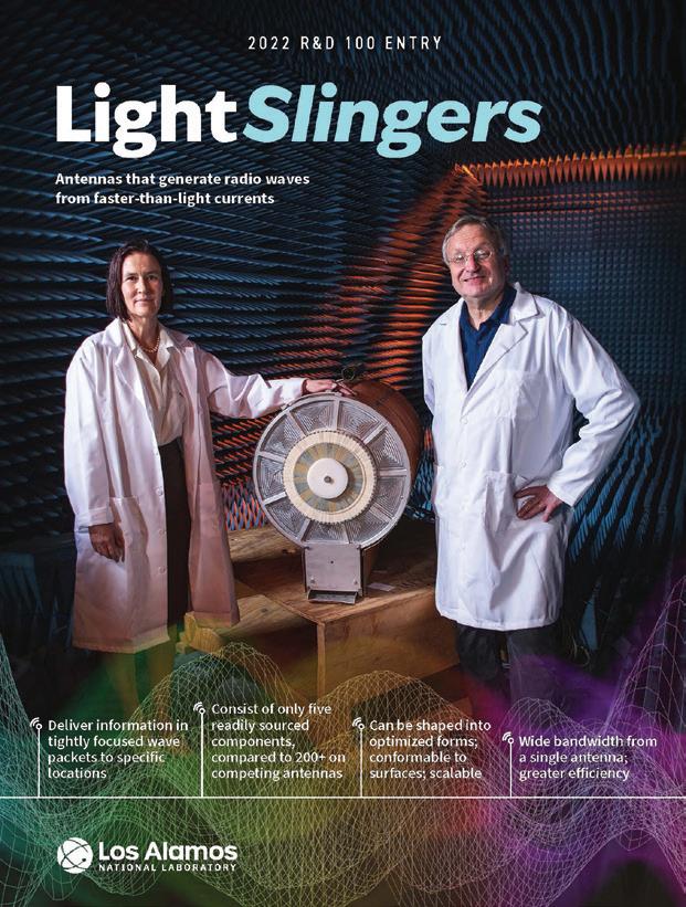
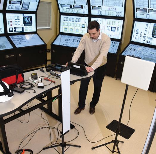
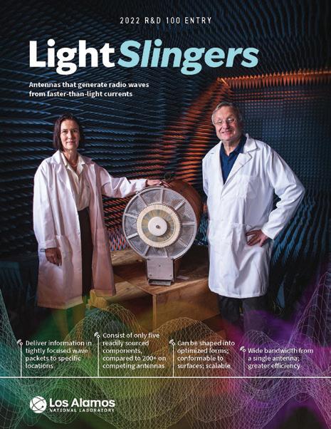
Creating a novel type of broadband antenna that generates radio waves from faster-than-light currents for broadcasting precisely toward a target location, providing better coverage, efficiency, bandwidth, and security, in a sturdier package with far fewer components.
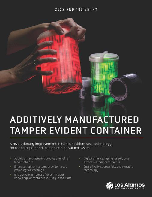
Applying additive manufacturing technologies for the simultaneous creation of a vessel and arbitrarily complexshaped three-dimensional tamper-sensitive features within its walls and lid to secure high value items from disclosure, theft, tampering, and espionage.
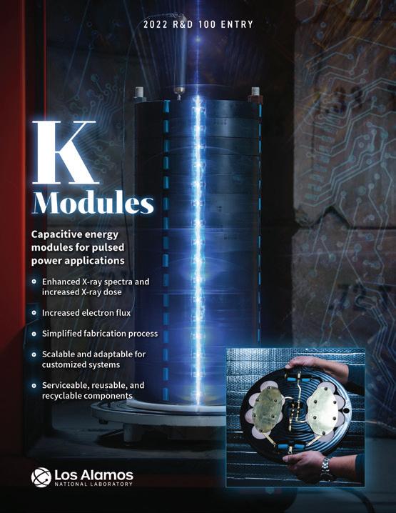
Developing an ultra-high resolution gamma spectrometer for nondestructive analysis of radioactive material in nuclear facilities, and capacitive energy modules to support pulsed power applications for X-ray and electron beam generating devices.
Producing nondestructive technologies for full-structure three-dimension nondestructive identification of subtle material flaws that can undermine integrity, and integrated sensors and software to detect damage and defects in large structures, regardless of size, complexity, or access limitations.


Providing tools for epidemiological decision support analysis, screening millions of possible biopolymer combinations for optimized materials, predicting metallic structural component behavior in extreme environments, delivering energyefficient machine learning for autonomous devices, and speeding scientific data analysis.
Visit our website www.lanl.gov/feynmancenter to explore the wide variety of technologies available.

Los























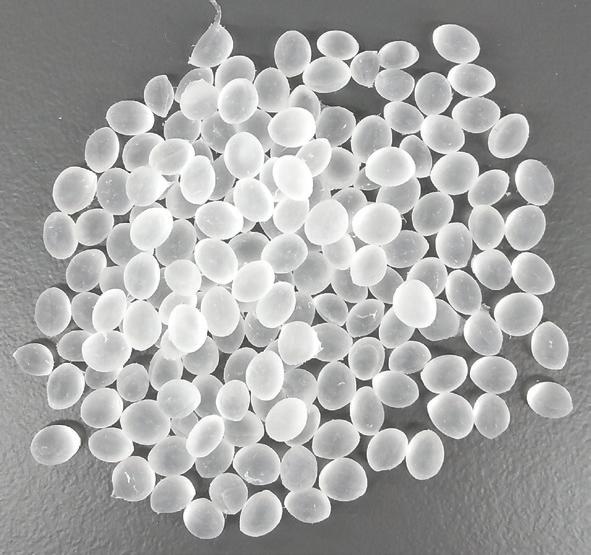
SABIC has commercialized an extensive portfolio of chemically upcycled LNP™ ELCRIN™ iQ materials to help support circularity. These polybuty lene terephthalate (PBT) resins can potentially serve as drop-in replace ments for conventional PBT to help manufacturers increase the sus tainability of end products. SABIC’s proprietary upcycling technology, which involves the repolymerization of discarded PET water bottles into PBT, delivers virgin-like performance properties. This process surpasses mechanical recycling in quality and consistency, and delivers important benefits such as colorability, including bright white colors.
LNP ELCRIN iQ resins, which use PET materials from different recycle streams, divert plastic waste from landfills and oceans (ocean-bound PET). To further enhance sustainability, these materials may incorporate pre-consumer recycled glass fiber. LNP ELCRIN iQ resins are candidates for consumer electronics applications, automotive seating, electrical connectors, and food contact applications such as personal care items, kitchen appliances and medical devices.
Advanced driver assistance systems (ADAS) are increasingly transitioning to higher-frequency radar (mmWave radar) to achieve better image resolution and greater range. To optimize transmission of mmWave radar, SABIC offers LNP™ THERMOCOMP™ WFC06I and WFC06IXP glass fiber-reinforced polybutylene terephthalate (PBT) compounds for radar front and back covers, and LNP™ STAT-KON™ WDF40RID compound for absorbers.
The LNP THERMOCOMP compounds deliver very low dielectric constant/dissipation factor (Df/Dk) performance and improved warpage control for thin-wall parts, both of which help enable transmission of higher-frequency radar signals. For efficient manufacturing, these materials provide laser welding capabilities.
The LNP STAT-KON compound is a new absorber material with controlled reflection. It can help reduce side lobe interference and ghost images to enhance signal purification. High flow enables thin-wall designs that optimize limited space within radar units and enable large designs outside radar units.

SABIC materials are helping to facilitate deployment of 5G networking infrastructure by enabling light weight, cost-effective all-plastic radio frequency (RF) antennas for base stations. LNP™ THERMOCOMP™ OFC08V compound, a glass fiber-reinforced polyphenylene sulfide (PPS) material, helps stream line antenna manufacturing and delivers critical properties including good warpage control, high heat resistance, and stable dielectric and RF performance. The material features excellent metal plating capability using laser direct structuring (LDS), which is simpler and faster than selective electro plating of traditional PPS resins. Strong adhesion between the SABIC compound and metal layers avoids delamination, even following thermal aging and lead-free reflow soldering.
The unique combination of properties offered by LNP THERMOCOMP OFC08V compound could enable injection-molded dipole antenna designs that provide advantages over traditional printed circuit board (PCB) assembly.


 LNP™ Mobility Electrical Products & Electronics
















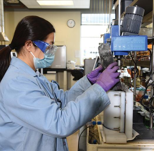


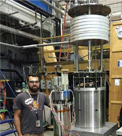


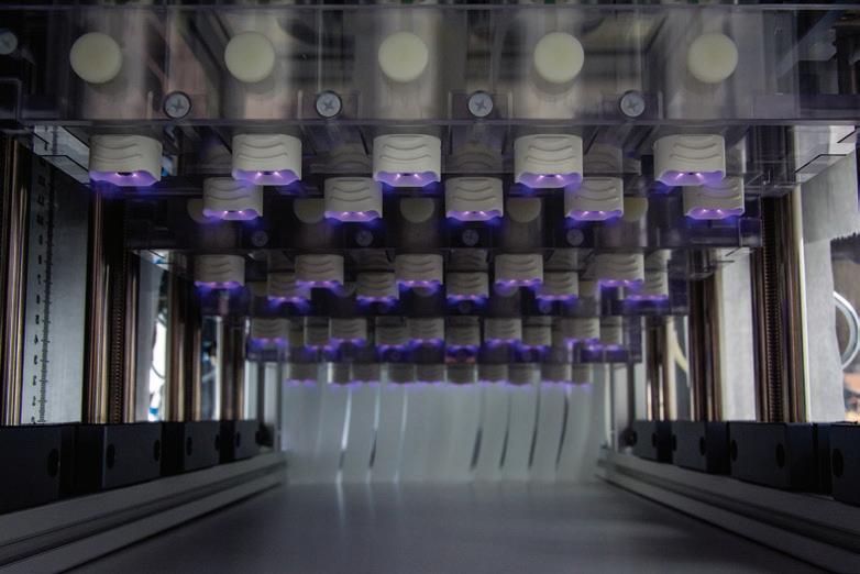


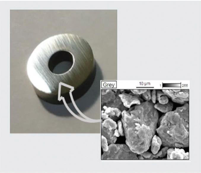


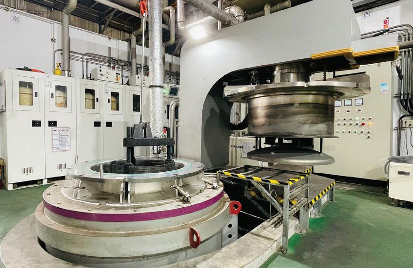
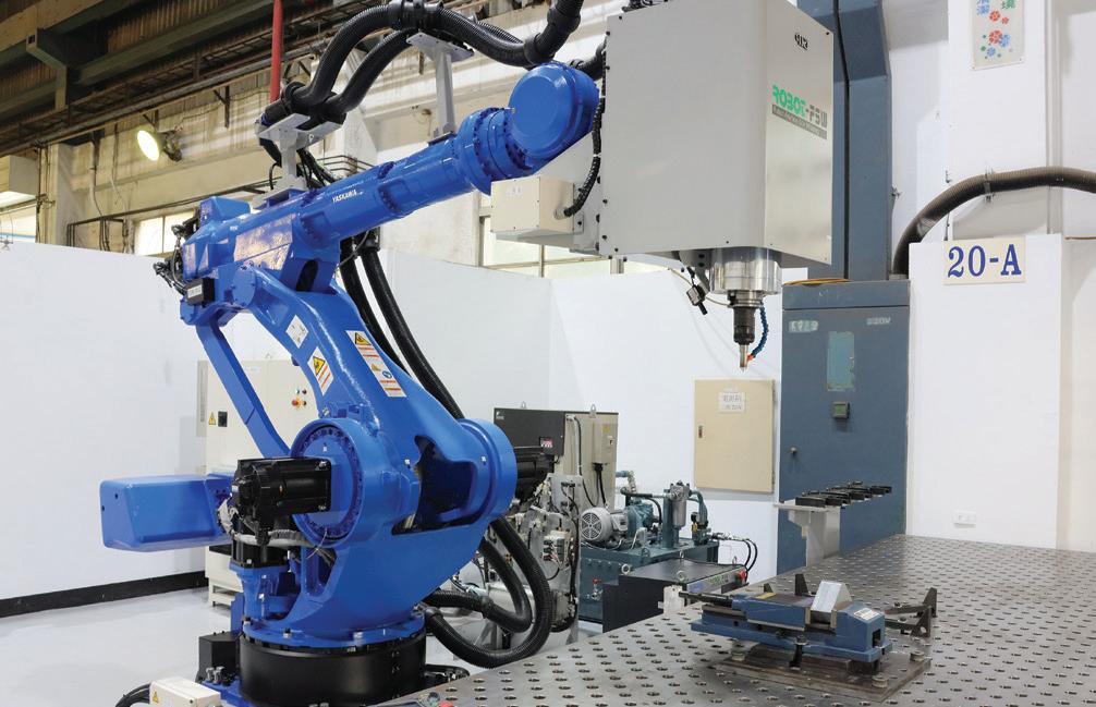
























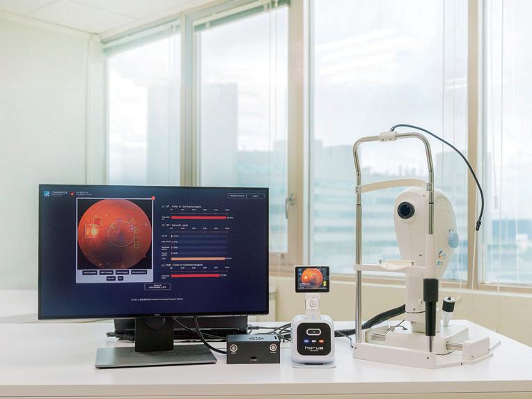


























Basestack: Enabling Crucial Genomics Work Around the World, Johns Hopkins University Applied Physics Laboratory
Calibrating Electrooculography Signals using Head Movements, MIT Lincoln Laboratory
Echo Revolution Microscope, BICO Group, Echo
In-Line Rapid Detection System for Dielectric Properties of MillimeterWave Materials (iLRD), Industrial Technology Research Institute (ITRI)
NanoPak-C All Carbon Stationary Phase Materials, Millennial Scientific nanoPOTS (Nanodroplet Processing in One pot for Trace Samples), Pacific Northwest National Laboratory
Non-Electric Infant Warmer to Save Neonatal Lives (DreamWarmer), Lawrence Berkeley National Laboratory, University of California, Berkeley; Boston Children’s Hospital; Partners In Health Center for Global Health Radar Scene Emulator, Keysight Technologies
The Argonne X-ray Perimeter Array Detector (XPAD), Argonne National Laboratory, Photon Science Directorate, Thermo Scientific Ultra-High-Speed Optoelectronic Interrogators (UltraSense) for Distributed Multi-Functional Fiber-Optic Sensing, Opterro, Inc., Intelligent Fiber Optic Systems (IFOS)
Caldera, Idaho National Laboratory
CommLess Microgrids: A Universal Design for Renewable Microgrid Resilience, National Renewable Energy Laboratory Common Evaluation Platform, MIT Lincoln Laboratory
Constrained Communication Cyber Device (C3D), Idaho National Laboratory Qubit Control System (QubiC), Lawrence Berkeley National Laboratory
Temporal Superconducting Digital Computing For Efficient Large-Scale Accelerators, Lawrence Berkeley National Laboratory, University of California at Santa Barbara
The Second Brain — The Next Generation Plug-and-play IIoT Device for i4.0 Application (Smart Patch), Hong Kong Productivity Council
Water Leakage Detection Sensor, Hitachi, Ltd.
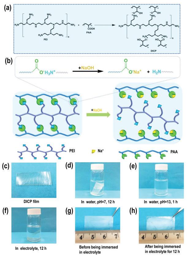
A High-Efficiency Carbon Nanotube-Coated Mesh Seal, Oak Ridge National Laboratory, Danfoss Turbocor Compressors Inc.
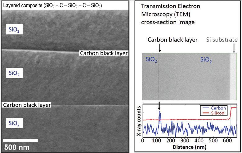
A Sustainable Anti-pilling Nano Coating for Wool Garment, Nano and Advanced Materials Institute, Laws Knitting Limited Advanced Graphene-Based Lubricants for High-Temperature Metal Stamping, Argonne National Laboratory, Magna International Inc. ArmourPrint by Under Armour: Durability and Performance Improvements of Active Wear enabled by Dow SILASTIC LCF 8300
Liquid Silicone Rubber (LSR), Under Armour, Dow Casting Mold with Controllable Defect Location, Metal Industries Research & Development Centre (MIRDC)
DOWSIL EC-8425 Electrically Conductive Adhesive: A Sustainable Solution for Advanced Electronic Devices, Dow Performance Silicones & Specialty Materials
DuPont Zytel HTN50Gxx series (HTN50G35HSL, HTN50G35FWS): from a new polymer backbone HTN500 PPA (Polyphthalamide) resin for Automotive Application, Mobility & Materials, Engineering Polymers, DuPont DuPont Zytel RS32G10DO Renewably-Sourced Low-Density Material for Light-Weighting Consumer Electronics, DuPont Mobility & Materials Energized DEF Mixer for Near Total Elimination of Toxic Diesel NOx, Emissol LLC
Fluorine Free Hydrophobic/Oleophobic Nano-shield Coating for EcoFriendly Paper Based Food Packaging, Nano and Advanced Materials Institute Imron Industrial High Performance Urethane Primer, Axalta Coating Systems Industrial Particulate Matter Terminator (IPMT), Industrial Technology Research Institute (ITRI)
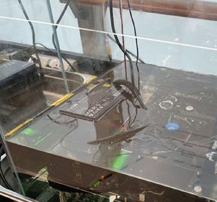
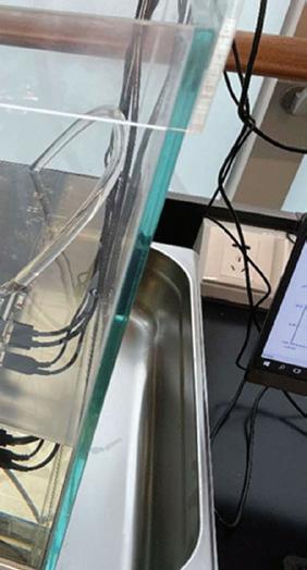
Innovative Solutions Enabling Efficient 5G and Enhanced Connectivity, Dow Packaging & Specialty Plastics, CommScope Low-Power, Fluorine-Free Micro Immersion Cooling technology for Data Center, LP2F-MIC, Industrial Technology Research Institute (ITRI)
PHORMANTO: New Polyethylene Rich Thermoforming Technology for the Fresh Poultry Market, Dow Packaging and Specialty Plastics, a business unit of Dow Inc.


32 Tesla Superconducting Magnet 32 4D (3D+Dissimilar) Printed of Solid State Process 36
Abcite 2060 Thermoplastic Flame Spray Powder Coating 19 Additively Manufactured Tamper Evident Container 16 Airborne Collision Avoidance System for Small Uncrewed Aircraft Systems 47
ALArM: Acoustic Large-Area Monitoring 44, 54
ASSESS: Acoustic Steady-State Excitation Spatial Spectroscopy 17 Automated Threat Estimator for Networks and Applications (ATHENA) 48
Battelle’s Process for Converting Coal to High-Value Polyurethane Products 33
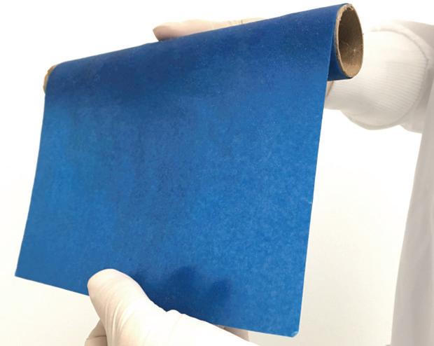
BioManIAC: Bioplastics Manufacturing with Intelligent Adaptive Control 18, 54 Black Magic Carpet for Water and Power Production (BMC-WP) 38 Brine Concentration with FilmTec Fortilife XC120 membranes 28, 54
CAPfresh — A Game Changing Cold Atmospheric Plasma Disinfection System for Fresh Food 33
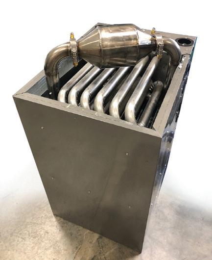
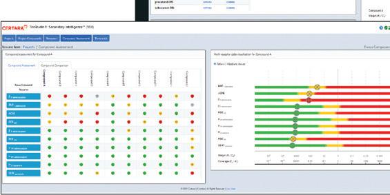
Catalytic Converter Needing Substantially Less Platinum 30 Certara’s Secondary Intelligence Software Predicts
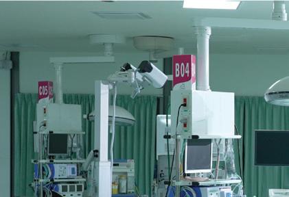
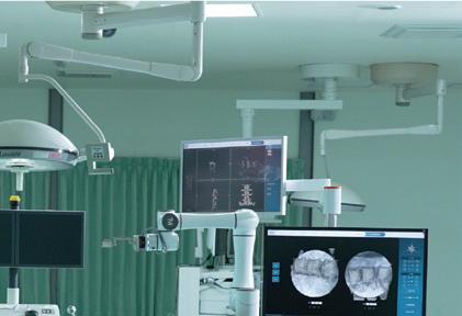
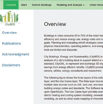
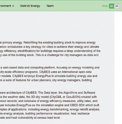
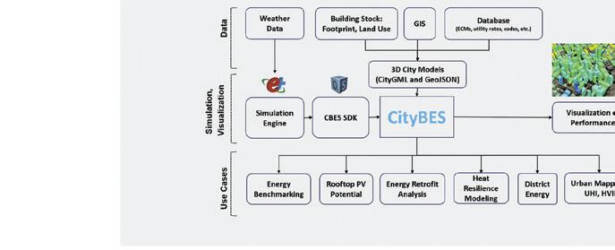
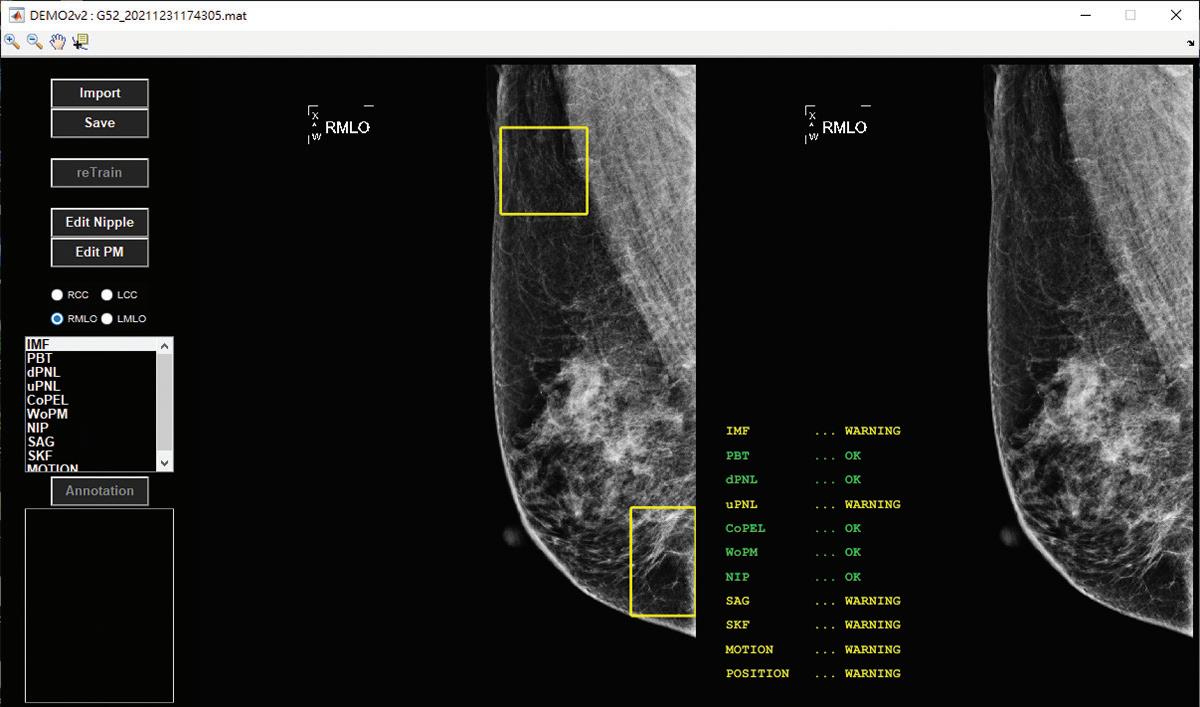
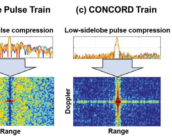
Likelihood of New Drug Candidates Causing Safety Concerns 42 City Buildings, Energy, and Sustainability (CityBES) Web Tool for Climate Change Strategies 39 Comex VINIMEX TOTAL Antiviral and Antibacterial 23, 52 Constrained Communications/Radar Dual-Use Waveforms (CONCORD) 45 Continuous Tracking Surgical Assistance System (CTSAS) 9
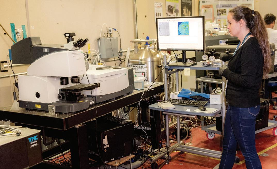
Corrosion-Resistant, Surface Hardening System Equipment for Austenite Stainless Steel 36 cryoRaman — Cryogenic Raman Microscope 9 Digital M functional resin material: Drops on where functionality is needed upon fabric 27
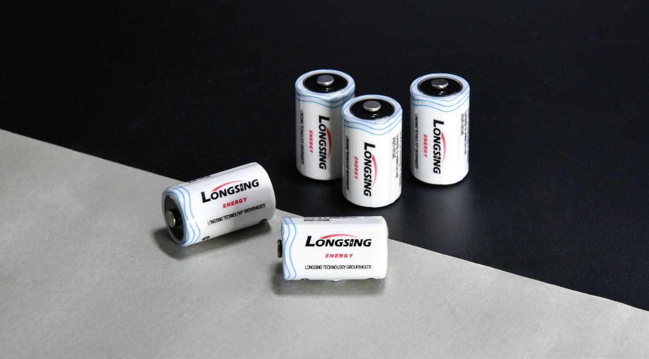
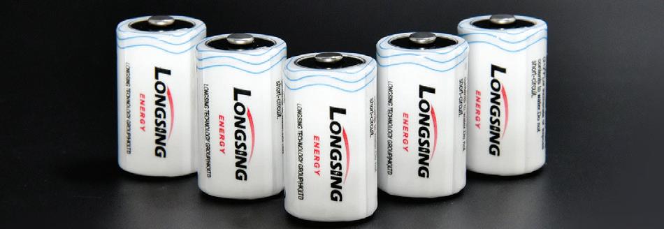
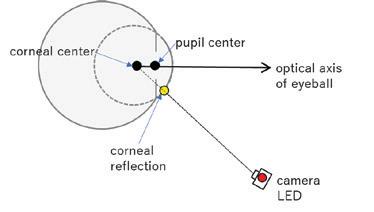
DOWSIL ICL-1000 Data Center Immersion Cooling Fluid 30 Drain-on-Demand Lithium Battery for Long-life IoT Devices 29 Driver Monitor System for Advanced Drive 47
DuAlumin-3D: An Additively Manufactured Dual-Strengthened 22 Aluminum Alloy Designed for Extreme Creep and Fatigue Resistance 22 DuPont BETATECH Thermal Interface Material 22
DuPont GreenTape 9KC LTCC and Ag metallization for mmWave 5G wireless devices 23
DURATRACK R-100 and AEH-100 Resins for Green Bike Lanes 20 Edge-AI Powered Multi-Sensor Aerial Inspector for Tunnel Surface 44 Electrochemical Leach (EC-Leach) 34
ELVALOY RET MF 1177 Polymeric Post-Consumer Recycle Asphalt Paving Compatibilizer 31
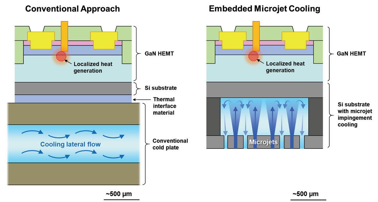
Embedded Microjet Cooling for High-Power Electronics 17
EpiGrid: A user-friendly tool for epidemiological decision making 41, 52 EVO PanHunter 41
Evusheld: A long-acting antibody combination for the prevention of COVID-19 in high-risk individuals 12, 52
Flash-X, a Multiphysics Simulation Software 48
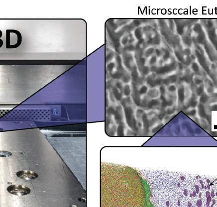
Full Field of View Atom Probe Microscope — The Invizo 6000 9 Green Machine — using hydrothermal technology to separate and recycle polyester and cotton blends 34
Gremlin: Discovering Weaknesses in Artificial Intelligence 39
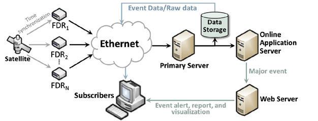
GridEye: A Wide-Area Power Grid Real-Time Situational Awareness System 42
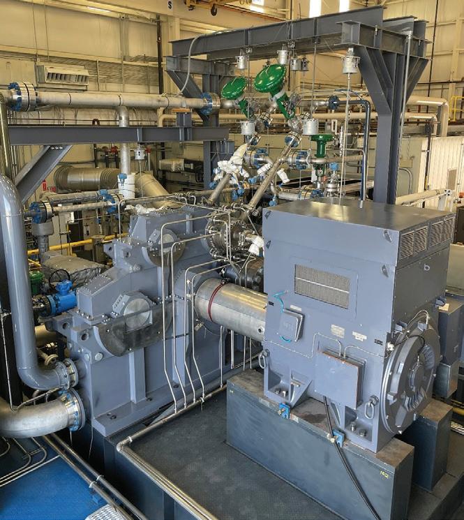
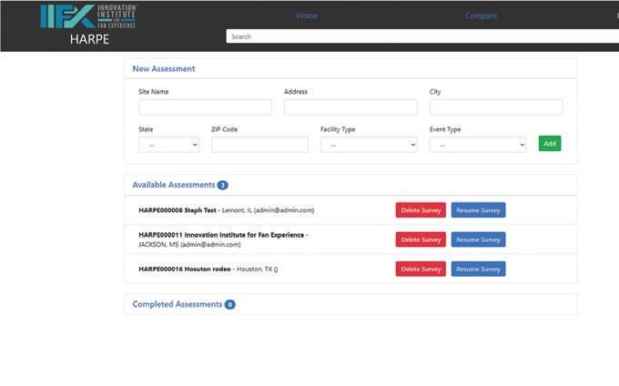
Hanwha Power Systems Integrally Geared Supercritical CO2 Compander 17 Health Analysis and Research for Public Events Tool (HARPE)
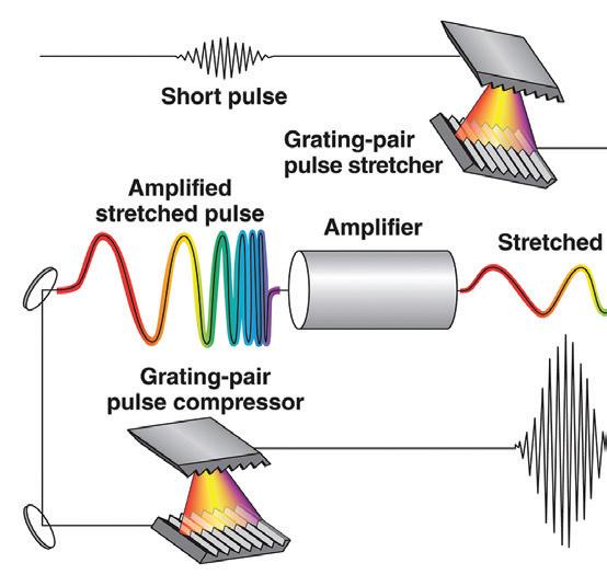
High Energy, Low Dispersion (HELD) Multilayer Dielectric (MLD) Gratings
High Resolution Full-Color micro-LED Display for AR Glasses

High-Power Bipolar Solid-State Battery
Hydra I/O: A system for highly resilient inter-chip communications
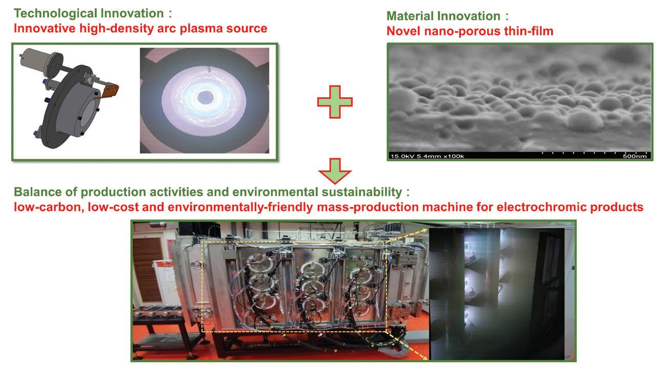
Innovative, low-cost and low-carbon technology for mass-producing electrochromic glass
Intelligence-Driven Cybersecurity Analytic Platform
Iron Nitride Soft Magnetics
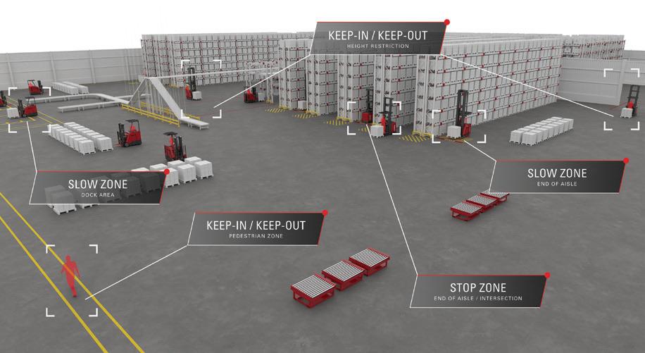
iWAREHOUSE® Real-Time Location System (iW.RTLS)
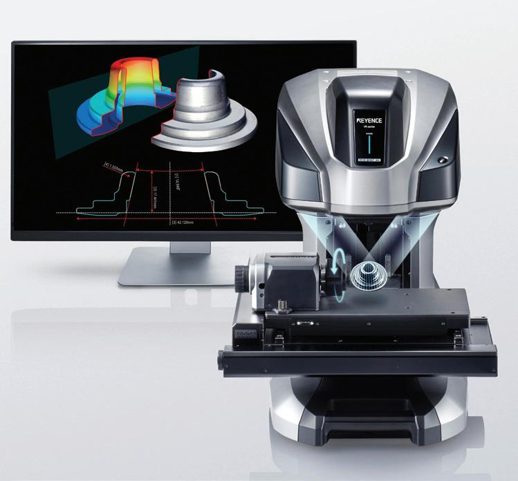
K-Modules: Capacitive Energy Modules for Pulsed Power Applications 13 KapFlo: Clear Polyimides without compromising High Temperature Stability for Next Generation OLED Smartphone Displays 28 Keyence 3D Optical Profiler with Rotational Unit 10
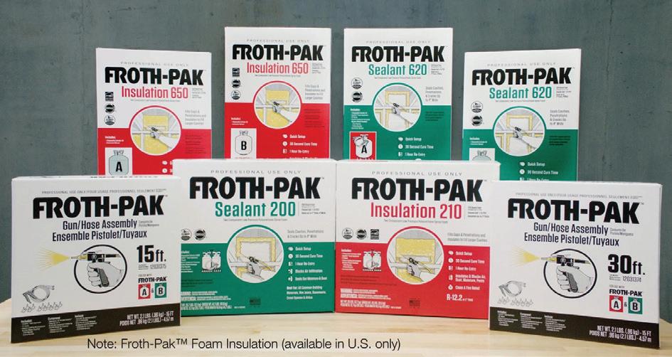
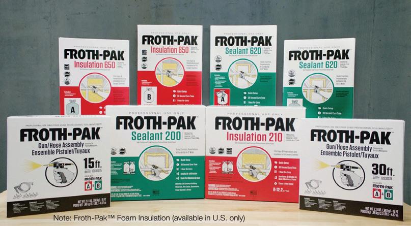
LightSlingers: Antennas that generate radio waves from faster-than-light currents 13, 53, 54 LNP THERMOCOMP OFC08V Compound, innovative material solution enabling the world first LDS antenna design for 5G infrastructure 19 Low GWP Froth-Pak Spray Foam 27, 53 Machine Intelligence for Review and Analysis of Condition Logs and Entries (MIRACLE) 50
MAINCOTE HG-300 Emulsion for high performance one component metal protective coatings 23 MaizeCare Clarity Polymer: A Sustainable, Superior Polymer for Clear Hair Styling Gels 22 Mammography Quality Evaluation (MQE) 41
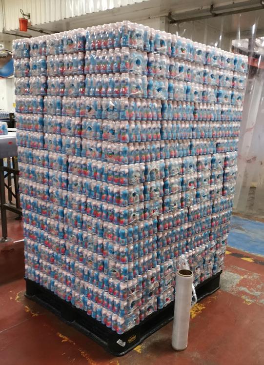
More sustainable Collation Shrink Film enabled by REVOLOOP and DOWLEX GM AX01 26, 53
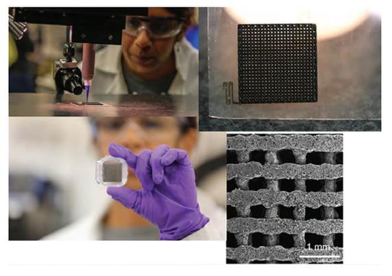
MOSAICS: Bringing the Future of Industrial Cybersecurity Into Focus 45 Multifunctional, 3D-Printable Inks for Energy Products (Energy Inks) 26 NuSense Technology — High Spatial Resolution Optical Sensors for Harsh Environments 10
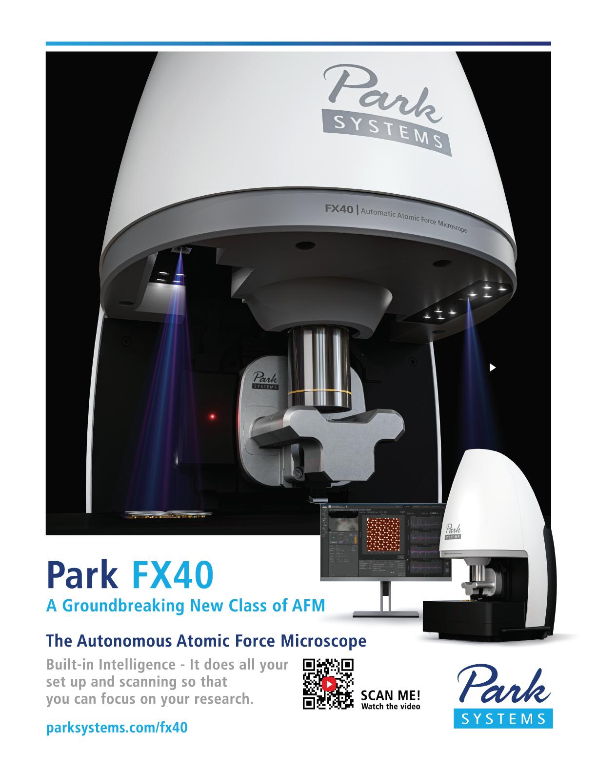
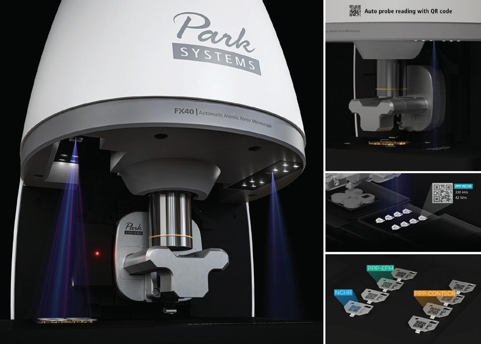
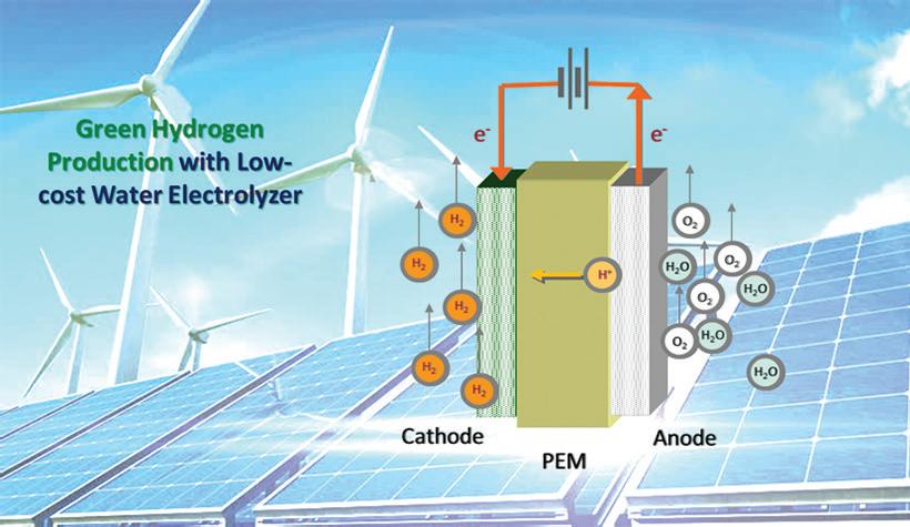
On-Chip Neuromorphic Backpropagation Algorithm 42 Park FX40 Atomic Force Microscope 10 PGM-free OER Catalyst as Replacement of Iridium for PEM Water Electrolyzer 20 Point-of-Care AI-DR 40
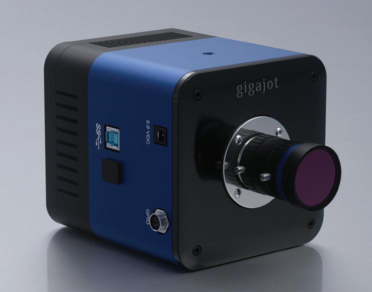
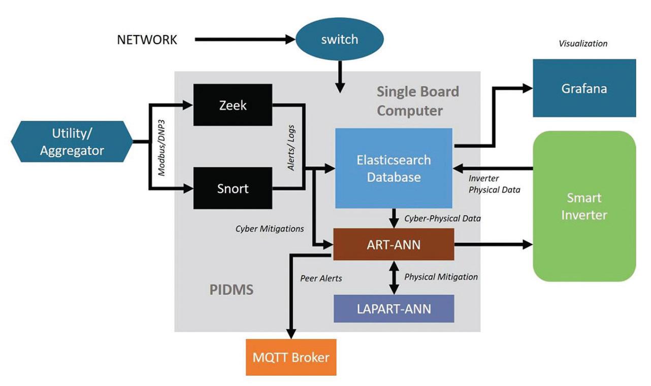
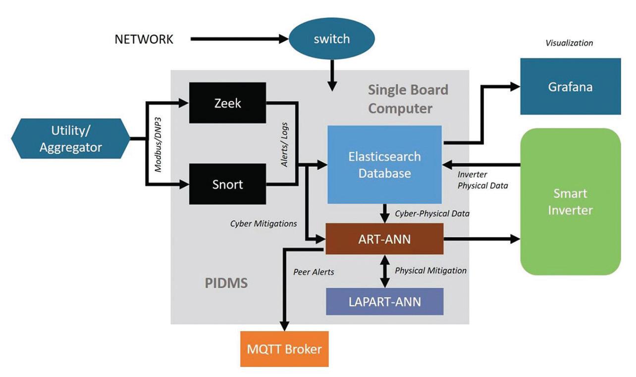
PPG COPPER ARMOR Anti-Viral and Anti-Bacterial Paint 27 Proactive Intrusion Detection and Mitigation System (PIDMS) 50, 54 proteoCHIP 11 Quanta Image Sensor (QIS) Camera 8 Quantum X bio 36 Quick-Release Binder for Recyclable Batteries 18 RapidCure: High-Speed Electron Beam Processing of Battery Electrodes 38, 54 Rate-Responsive Smart Bandage for Sport Injury Prevention 21
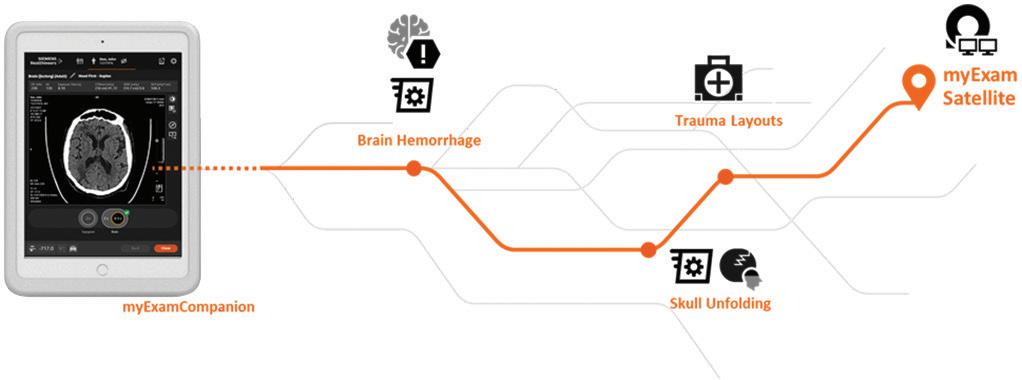
SABIC’s LNP ELCRIN iQ Upcycled Product Portfolio Contributing To Net-Zero Carbon Goals In Multiple Industries 26 SABIC’s Technology Breakthrough and Advanced Compounds Helping ADAS Designers Improve Signal Transmission Accuracy & Reliability 31 Safety & Reliability with Silicone Solutions for Electric Vehicle Thermal Management 21 Siemens Healthineers Intelligent Emergency Imaging 39
SILVTEA Multi-Applicable Silver Conductive Ink 37
SOFIA: Spectrometer Optimized for Facility Integrated Applications 13
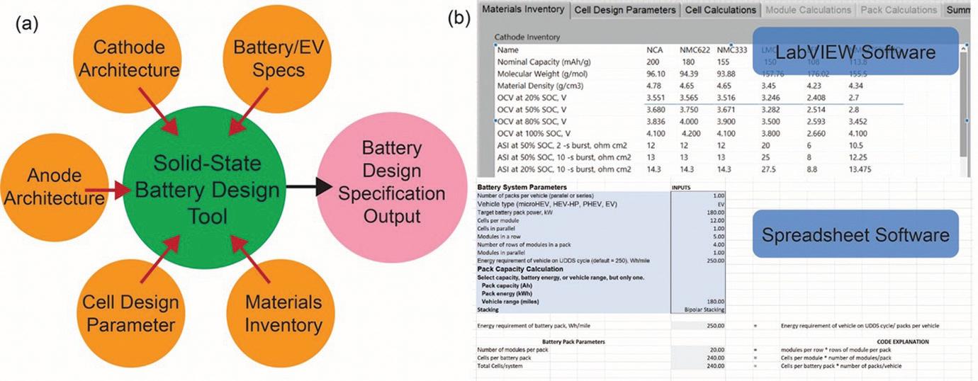
Solar Fuel Generator Including a Catalytic Mesh 19 SolidPAC: A Comprehensive Solid-State Battery Design Tool 48 Spectral Phenotyping with MirroRx 8 Stable and High-Performing Single-Crystal LiNixMnyCo1-x-yO2 Cathode Materials (SC-NMC) 28
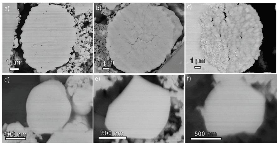
Tailored Glass Using Direct Ink Writing Technology 38
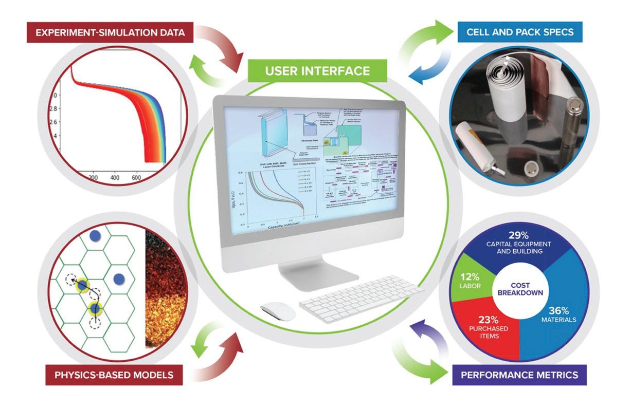
The Battery Performance and Cost (BatPaC) Model 45
The SEED Platform: Decarbonizing Cities Through Robust Data Management 44 Thermo Scientific Gallery Enzyme Master Enzyme Analyzer 12 Thermo Scientific Orbitrap Exploris MX Mass Detector 11 Timely Address Space Randomization (TASR) 47
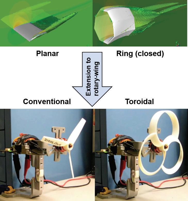
Toroidal Propeller 29 TROPICS Pathfinder Satellite 33 Ultra-Stable Thermally Excellent Advancements in Material Strength (USTEAMS) 20
Ultraclean Condensing Gas Furnace 18 UniTOM HR Dynamic Micro-CT System 8 VK-X3000 3D Surface Profiler 11





The Institute for Information Industry (Cybersecurity Technology Institute/CSTI) has reported that hackers’ intrusions into critical infrastructure are primarily caused by a lack of the attack chain identification technology that incorporates real-time intelligence and artificial intelligence. Using A technology, CSTI develops a comprehensive “Intelligence-Driven Cybersecurity Analytic Platform” using virus pattern analysis, VADER sentiment analysis, and kill chain analysis to identify hackers for cyber attacks on track prior to information security threats.


The platform has built-in self-developed AI-assisted malicious behavior detection model, which has been able to grasp up to 91% of ransomware through


evaluation. In addition, it also provides a userfriendly UI operation interface. As long as you select the detection file, you can scan the service through the API, automatically compile the information security detection result report, master all-round file information, and effectively prevent the occurrence of ransomware threats.


In response to the rampant spread of ransomware, the “Intelligence-Driven Cybersecurity Analytic Platform” is working with financial startups to create a zeroransomware cloud service environment for fighting against “Ransomware-as-a-Service (RaaS)” developed by hackers.

Hackers have no way to hide! The award-winning technology by Cybersecurity Technology Institute from Institute for Information Industry “Intelligence-Driven Cybersecurity Analytic Platform”
CAMECA experts answer your questions.
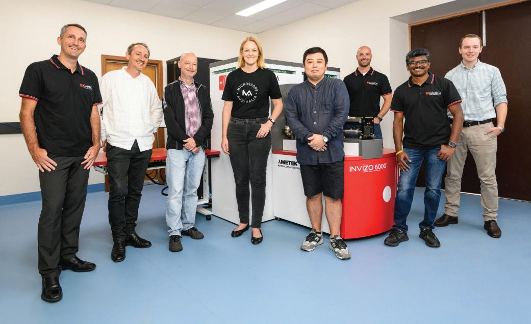
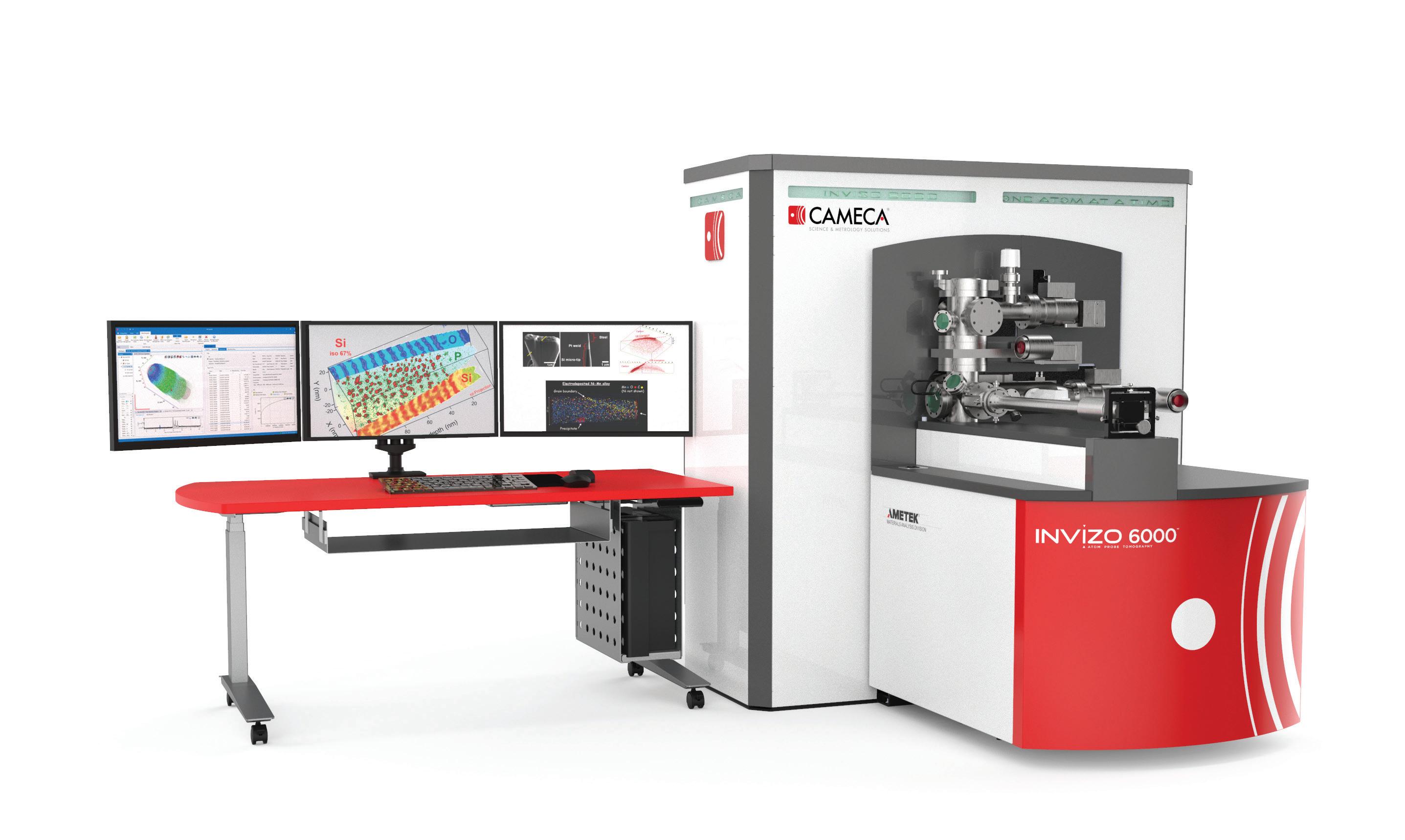
The Invizo® 6000 is a 3D atom probe with the largest field of view, highest single-specimen yield, greatest analysis volume and most accurate reconstruction, regardless of application.
When it comes to Atom Probe Tomography (APT), breakthrough advances seem to arrive about every 15 to 20 years. From the exciting advent of APT in 1967 and 3D atom probe in 1987, to the introduction of laser-assisted Local Electrode Atom Probe (LEAP) in 2003 and Focused Ion Beam (FIB) in 2005, what surprises can the next generation possibly have in store?
For one, a surprisingly robust technology that takes CAMECA’s LEAP 5000 to a whole new level. Derived from the Latin viso, or view, the Invizo 6000® 3D Atom
Probe microscope opens vast new horizons of research. So much so that the 2022 R&D 100 Awards has named “Full Field of View Atom Probe Microscope — The Invizo 6000” a winner in its Analytical/Test category.
“The Invizo 6000 is a highefficiency, symmetric dualillumination, DUV laser APT microscope providing 3D subnanometer spatial resolution information for all elements. It provides the widest field of view and the fastest data collection rate of any APT system to solve the most challenging materials problems,” states the
R&D 100 Awards, a globally renowned science and innovation competition.
“This newest generation of 3D atom probe is capable of capturing the entire internal volume of users’ specimens,”
APT Senior Product Manager Robert Ulfig said. “Among the key features of Invizo 6000 are a wide field of view and innovative electrostatic flight path. Others are its DUV wavelength and dualbeam illumination,” Ulfig added. (See Q&A below for more.)
Following the introduction of LEAP, APT has become a standard material characterization method enabling 3D nanoscale compositional characterization of metals and alloys, ceramics, semiconductors, biomaterials and geological materials. Since developing LEAP, CAMECA has remained at the forefront of APT and Secondary Ion Mass Spectrometry (SIMS) instrument design. Major new features of Invizo 6000 promise to accelerate advanced research in both academic laboratories and manufacturing facilities worldwide.
Invizo 6000: The only 3D atom probe capable of capturing the entire internal volume of specimens.
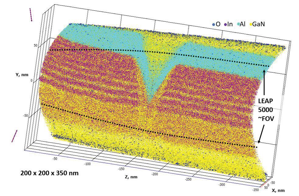
Analysis of a GaN multi-quantum well LED device demonstrating the benefits of Invizo 6000’s full field of view optics.
to improve both in the same patented design. This enables imaging the full specimen volume while maintaining excellent spectral quality that makes both specimen preparation and data analysis faster and easier. In addition, the flight path design allows symmetric illumination of the specimen with the laser, further improving data quality.
What is important about the new technique’s DUV laser wavelength feature?
A threading dislocation is captured across the superlattice, quantum wells and AlGaN blocking layer — all visible within a single image thanks to the Invizo 6000’s ability to capture the entire field evaporating volume, as shown by the native oxide layer visible at the surface.
This includes the capability of increased analysis volumes that capture larger features of interest and improve analytical measurements for a diverse set of applications such as metallurgy, geoscience, energy materials and semiconductors.
CAMECA has partnered with the University of Sydney to research Invizo 6000’s field of view and resolving power capabilities across a range of materials science areas — from additive manufacturing and catalysis to photovoltaics and Martian meteorites.
APT is the most powerful subnanometer spatial resolution 3D compositional technique available. APT changes the very definition of “microscope.” While microscopes are instruments for making enlarged images of minute objects — that’s not how
APT works. The question then becomes, is the new Invizo 6000 a microscope or a data collection device?
CAMECA APT experts Robert Ulfig (RU) and David Reinhard (DR) answer this and other frequently asked questions about Invizo 6000 features and how it pushes the boundaries of APT:
It’s been said that in APT, “the software is the microscope.”
What are some unique software features of Invizo 6000?
DR: APT is a truly unique microscopy, as once the data have been reconstructed into a computer model, the analyst has a chemically resolved, atom by atom map of the specimen in 3D, at which point detailed data interrogation can begin.
Isoconcentration surfaces and thin clipping planes can be used to quickly scan for inhomogeneities that can
highlight key microstructural features. Once identified, tools such as 1D composition profiles, 2D contour plots, radial distribution profiles and cluster analysis can quantify the composition variation across these features. Regions of interest can also be arbitrarily defined to isolate specific volumes for detailed mass spectral analysis. Automated peak identification and peak overlap decomposition tools are provided to help quantify local compositions.
What are some specific features of the new APT technique’s ultra-wide field of view and innovative flight path?
RU: Traditional time of flight microscopy typically includes significant tradeoffs in mass resolving power and sensitivity when optimizing the field of view. Our research and development team was able
RU: While developing the innovative technology of LEAP system in 2003, we knew that the expansion into non-conductive specimens would require laser pulsing. Since our introduction of the first commercially available laser pulsing system — a 2004 R&D 100 Award recipient— we have worked with many different lasers moving from longer wavelengths (visible light spectrum) to UV and DUV lasers. (See sidebar below for additional R&D 100 Awards earned by CAMECA.)
• 1993 — Position-Sensitive Atom Probe (PoSAP): The first commercially available microscope providing 3D quantitative, subnanometer data.
• 2004 — LEAP: 20,000 times faster, 20 times mass resolving power (MRP), 25 times field of view (FOV).
• 2006 — LEAP 3000X: For green laser, new materials.
• 2008 — LEAP 3000X HR: For reflectron MRP, sensitivity.
• 2015 — LEAP 5000 product line: For UV laser and tight focus, enabling new applications.
• 2022 — Invizo 6000: For FOV, DUV, dual-illumination, new materials and applications.
Ultra-wide
Our research has shown that the higher photon energy (shorter wavelength) is absorbed more efficiently and evenly by atom probe specimens. Not only do the shorter wavelengths get absorbed more evenly by different materials, they allow for a tighter focused spot that results in very rapid heating and cooling of the specimen apex. This means that the field evaporation occurs over a very short period of time. For time-of-flight microscopy, this means better mass spectral quality, which means higher sensitivity. Working with shorter wavelengths comes with design challenges, but the clear benefit to the user makes overcoming every challenge worthwhile.
What is special about the technique’s dual-beam illumination?
RU: Asymmetric laser illumination can result in asymmetric field evaporation, the process that enables single atom at a time analysis. The dual beam illumination enabled by Invizo’s innovative flight path means that the specimen can absorb laser energy more evenly and therefore field evaporate more evenly.
This means a higher data quality in all three dimensions of the reconstruction, which leads to data analysis that is more straightforward and accurate. The APT community thought this would make the operation of the system more complicated, but in reality, running the system is easier than ever. Many steps in the process have been fully automated, allowing users to concentrate on problems that can be solved with APT — without having to spend valuable time on system operations.
In conclusion, how do the above key features benefit different applications?
RU: The key features of DUV, symmetric illumination and full field of view translate directly to a faster time to knowledge across all applications. Working with a world-class team like the University of Sydney means that we can use atom probe data synergistically with their entire suite of instruments – enabling new ways to look at the data. The wide field of view makes the data more useful when correlating it with other techniques such as transmission electron microscopy. Of course, adding in the inherent 3D quantitative analysis of APT means being able to solve problems that, until now, had not been considered.
Robert Ulfig is senior product manager for APT. He brings expertise in materials science and semiconductor manufacturing and technology to product development worldwide. He also provides training to engineering, software and manufacturing professionals on CAMECA’s software and hardware.
David Reinhard is product manager for APT. With a background in materials science, he spent over a decade in CAMECA’s applications lab analyzing materials with the atom probe and presenting the results to researchers worldwide. As product manager, he helps guide the development of the technique in an effort to expand the boundaries of atom probe analysis.
“THIS NEWEST GENERATION OF 3D ATOM PROBE IS CAPABLE OF CAPTURING THE ENTIRE INTERNAL VOLUME OF USERS’ SPECIMENS.”
— APT SENIOR PRODUCT MANAGER ROBERT ULFIG
DUAL ILLUMINATION,
• Atom Probe Tomography user’s website, by CAMECA. (www.atomprobe.com.)
• Atom Probe Tomography Webinar Library, by CAMECA. (www.cameca.com/company/news/2021/october/new-webinar-series-on-apt.)
• ATOM PROBE 3D: Invizo and LEAP 6000XR Launch Event, by CAMECA. (www.youtube.com/watch?v=IFgk6ZsnvQQ.)
• David A. Reinhard, Daniel Lenz, Isabelle Martin, Ty J. Prosa, Robert M. Ulfig, Peter H. Clifton, Brian P. Geiser, Joseph H. Bunton and David J. Larson. Invizo 6000, New Applications, New Performance, by CAMECA Instruments Inc., Madison, WI, USA. Corresponding author: David.Reinhard@AMETEK.com. (www.cambridge.org/core/journals/microscopy-and-microanalysis/article/new-product-announcementinvizo-6000-new-applications-new-performance/70C4D0A50106D50F785B416B2273B07E.)
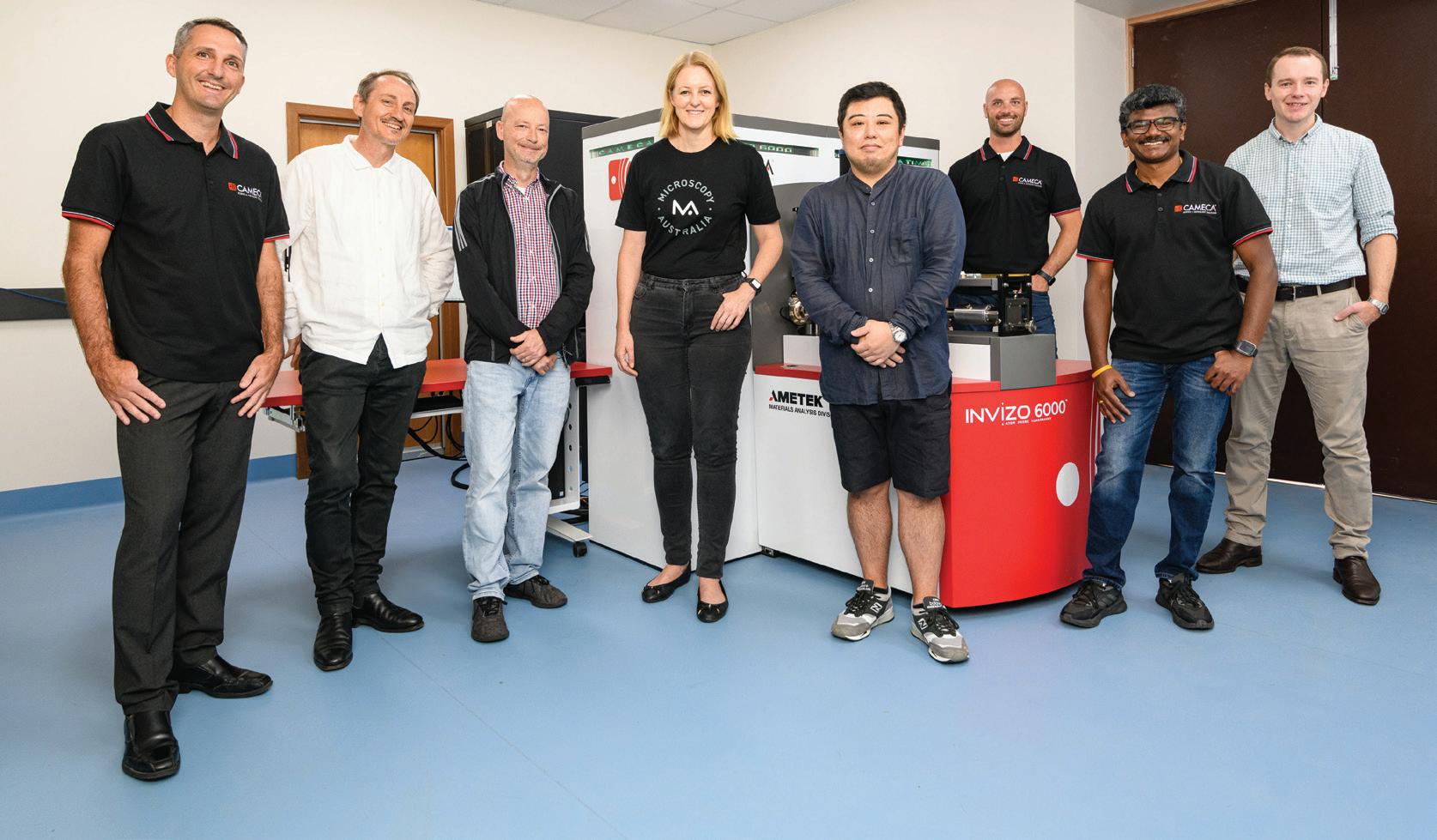
CAMECA, a business unit of AMETEK, Inc., is a leading global supplier of a diverse range of advanced characterization technologies for government, academic, and industry research and process control. CAMECA provides customers with the highest analytical performance in their specialized characterization fields. This includes development of scientific instrumentation for R&D professionals, as well as in-fab and near-fab metrology solutions for the semiconductor manufacturing industry. With headquarters near Paris, France, and an Atom Probe Technology Center in Madison, Wisconsin, CAMECA employs best practices for computer networking, electron and ion optics simulation, and advanced CAD. The CAMECA APT product line comprises the 6000 series platform. CAMECA is a recipient of multiple R&D 100 Awards, including a 2022 win for its Invizo 6000 3D Atom Probe microscope.
THE WIDEST FIELD OF

AND
FASTEST DATA
RATE OF ANY APT
THE MOST

R&D


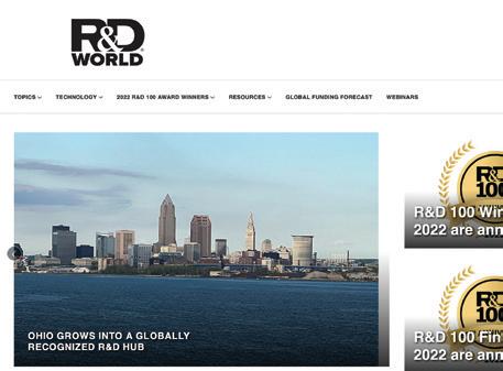
With top-notch universities, federal research institutes, leading companies from nine major industry sectors, and 14 top-ranked hospital systems, Ohio is a “quiet giant” of innovation in industrial sectors and life science. Ohio has the fifth-highest number of Fortune 500 and Fortune 1000 companies — and is home to more than 120 NYSE/Nasdaq companies with a combined market capitalization exceeding $1 trillion.
Ohio government executives attribute the state’s growth to government actions that help businesses succeed and the research and development (R&D) investments that lay the foundation for innovation in the Midwest.

In 2019, government leaders challenged JobsOhio, the state’s private economic development corporation, to uncover new opportunities to enhance innovation within the state. JobsOhio saw a need for comprehensive initiatives that advance growthenabling innovation and bring in companies and highly skilled
By Gordon Fellertalent. In collaboration with the state government and healthcare and university partners, JobsOhio launched a three-pronged innovation strategy for Ohio.
Through partnerships with leading research institutions, universities, private corporations, and local, regional, and state economic development leaders, Ohio is developing nationally competitive innovation districts in the dense urban settings of Cleveland, Columbus, and Cincinnati. Each location has a priority focus based on the city’s existing institutions and expertise.
The world’s top people and companies come to these sustainable ecosystems of ideas, infrastructure, and talent to roll up their sleeves, create, and grow. With more than $3 billion in innovation district investments, they anticipate more than 47,500 new STEM graduates, 60,000 new jobs, and up to $9 billion in annual economic impact for the state over the next 10 years.
The Cleveland Innovation District is home to a global center for pathogen research and human health aligned with the $100 billion
biotech industry. This innovation district is anchored by the Cleveland Clinic — the No. 2 ranked hospital worldwide — along with Case Western Reserve University, Cleveland State University, MetroHealth Medical Center, and University Hospitals.
To the south, Cincinnati’s healthcare thought leaders are furthering Ohio’s global presence in pediatric oncology research and treatment. The city’s innovation district is anchored by the University of Cincinnati and Cincinnati Children’s Hospital Medical Center — the No. 3 pediatrics hospital in the country. Investments there are expected to spin out discoveries and companies to serve the $150 billion global pediatric healthcare market.
The Columbus Innovation District’s mission is to promote interdisciplinary research and high-tech therapies to address adult oncology. Anchored by The Ohio State University and Nationwide Children’s Hospital — the No. 8 pediatrics hospital nationally — Columbus will attract leaders and spark innovations in the $1.2 billion photon therapy market and the $3.4 billion global gene therapy market.
JobsOhio’s brain trust of industry leaders developed the Research & Development Center Grant Program to help business partners establish corporate R&D hubs equipped with tools and resources to build, disrupt, and drive growth globally. The resulting capital investments, trailblazing technologies, and innovative products align with the state’s strategy to attract and augment targeted industries while changing the world for the better by directly and positively impacting people’s quality of life.
There has been substantial interest in the R&D Center Grant Program, with inquiries from some of the most prominent domestic and international companies. So far, JobsOhio has committed approximately 20 R&D Center Grants, totaling $57.5 million, with companies investing $460 million and creating nearly 1,000 new jobs.
The third pillar of JobsOhio’s innovation strategy is a Growth Capital Fund that makes individual investments into Ohio-based, early-stage, venture-backed companies. By taking minority stakes under the same
terms as venture capital firms, JobsOhio helps early- and growth-stage companies become the next titans of their industries while remaining in Ohio — a state with the fourth lowest cost of doing business. And by all accounts, it’s working.
The Growth Capital Fund program has been a success. In 2020, Ohio was No. 17 out of 17 peer states for venture capital investments. The following year, it was No. 10 out of 17, with a record $2.4 billion of venture capital attracted. And in Q1 of 2022, when investments across the country slowed, Ohio attracted more than $900 million.

Thus far, JobsOhio has invested $87 million in 59 companies, leveraging other investment dollars at a rate of $6 of private capital for every $1 of JobsOhio capital invested. And after exiting just three companies so far, JobsOhio’s return on investment (ROI) has increased 2.8 times with an annualized ROI of 169%.
Ohio’s diverse industry outpaces its peers Ohio’s industrial footprint is growing through the R&D efforts bolstered by JobsOhio’s innovation strategy. The state ranks in the top 20% for industrial diversity, improving yearly since 2013 at the fastest pace among Midwest peers and quicker than many of the largest coastal states.
Semiconductor manufacturing Semiconductors are a critical part of modern life, and our increasing reliance on them is astounding. Yet semiconductor production has decreased, which strains the global supply chain. Impressed by the state’s welcoming business climate and stellar workforce, Intel chose to plant its flag in Ohio, building its next-generation chip fabs and supporting ecosystem. Intel’s initial $20 billion investment and suggestion that it could grow to $100 billion will establish what Intel calls the “Silicon Heartland.” If successful, it will help prevent the recurrence of chip-related disruptions that have negatively impacted the security of millions of jobs.
Intel’s manufacturing campus on nearly 1,000 acres in central Ohio will become the company’s most advanced semiconductor manufacturing operation. The construction will create about 7,000 jobs and 3,000 permanent, skilled, high-wage positions.
The project will have a massive direct impact on the state’s supply chain infrastructure and will be a catalyst for R&D across the region.
“We are excited to call Ohio home to Intel’s first new manufacturing site in 40 years,” said Pat Gelsinger, Intel’s CEO. “We expect Intel Ohio will become one of the largest semiconductor manufacturing sites in the world over the next decade.”
Novagard Solutions is one example of a corporation using a JobsOhio R&D Center Grant to attract, retain, and train talent needed to continue its track record of cutting-edge innovations. As a direct result of the grant, this woman-owned company expanded its silicone coatings and adhesives manufacturing operations with 50 new jobs in northeast Ohio and grew its revenue by $42 million.
In June 2022, Ford Motor Co. announced a $1.5 billion investment to convert its assembly plant in Avon Lake, Ohio, and expand production of an all-new line of commercial electric vehicles (EVs). In addition to the 1,800 new union jobs this will create, Ford also announced an additional 90 jobs and a $100 million investment between its Lima Engine Plant and Sharonville Transmission plants.

JobsOhio and its statewide partners worked over the past several years to build on the state’s momentum as one of the world’s major automotive sector hubs and as home to crucial, enabling technologies. For example, SEMCORP, the world’s largest lithium-ion battery separator film producer, is bringing its first U.S. facility to Ohio, propelling Ohio to the forefront of the EV industry. And Ultium Cells, a joint venture between LG Energy Solutions and General Motors (GM) to mass produce lithium-ion batteries for GM, is expected to begin production later this year. The Ultium Cells facility is one of the largest cell manufacturing plants in the world.
JobsOhio R&D Center Grants have supported intellectual property that accelerates the development of autonomous and EVs
since before 2018. They awarded $2 million to Pillar Technology to establish a collaborative space to accelerate the advancement of revolutionary intellectual property related to the development, testing, and validation of connected, autonomous EVs.
With the seventh largest U.S. solar labor force and rapidly growing penetration of solar energy, Ohio is attracting companies that aim to generate or use clean energy. Ohio currently has more than 8,400 mW of utilityscale solar projects either operating, approved for construction, or pending before the Ohio Power Siting Board for approval. The growing solar presence in the state can serve as a key investment attraction asset as major industries seek to decarbonize their supply chain through local renewable energy purchases. Promoting Ohio’s renewable energy presence in parallel with JobsOhio’s successful battery supply chain development efforts will lead to network effects for future investment attraction. Furthermore, Ohio government executives recognize a growing need to focus on mobility, sustainability, digitalization, and emerging
urban technologies. The SMART Columbus program addresses growing inequity, climate change, and technology disruption, aiming to achieve carbon neutrality by 2050 and to fully immerse all residents in the digital experience. Smart Columbus Program investments are expected to generate an increase of 4,220 jobs, 719 resulting directly from programrelated staffing expenditures and 3,501 from the program’s indirect effect on targeted industry sectors. Some accomplishments of the program include a transition to mobile payment for parking across Columbus, more than 900 additional electric vehicle charging stations, and a 500% increase in EV adoption, which placed Columbus at No. 3 among nonzero-emission-vehicle states for EV adoption.
State leaders are working to increase broadband coverage throughout the state, giving Ohioans faster and more reliable access to the internet. These broadband initiatives are expected to create 20,000 jobs in Ohio and a $1 billion increase in Ohio’s GDP.
Ohio’s data centers are just another way Ohio is diversifying its economy. The 26 enterprise data centers and 97 co-location data center sites power some of the most well-known companies in the world: Facebook, Honda, JP Morgan Chase, CitiGroup, and Amazon Web Services.
In April 2022, Facebook’s parent company, Meta, announced it would expand its data center in New Albany, Ohio, by 1 million sq-ft. The expansion will boost Meta’s investment in New Albany to $1.5 billion and house the data for billions of users using Facebook, Instagram, Messenger, and WhatsApp.

“So, whether you’re sharing photos, video, or reels on Facebook or Instagram, the New Albany data center has a huge impact on bringing the world closer together,’’ said Katie Comer, Meta’s manager of the community development team in North America.
A rise in chronic disease, the nation’s aging population, and the global pandemic have accelerated the need for medications and triggered an urgency for innovative solutions.
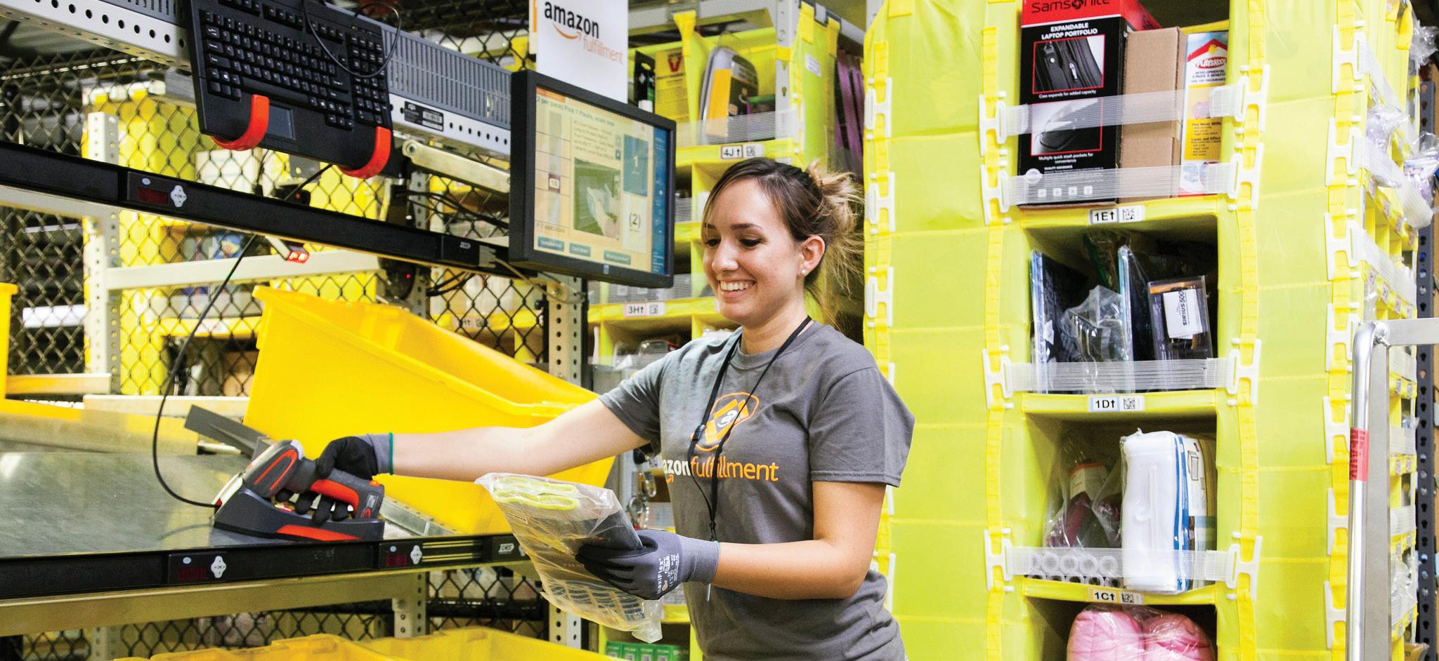
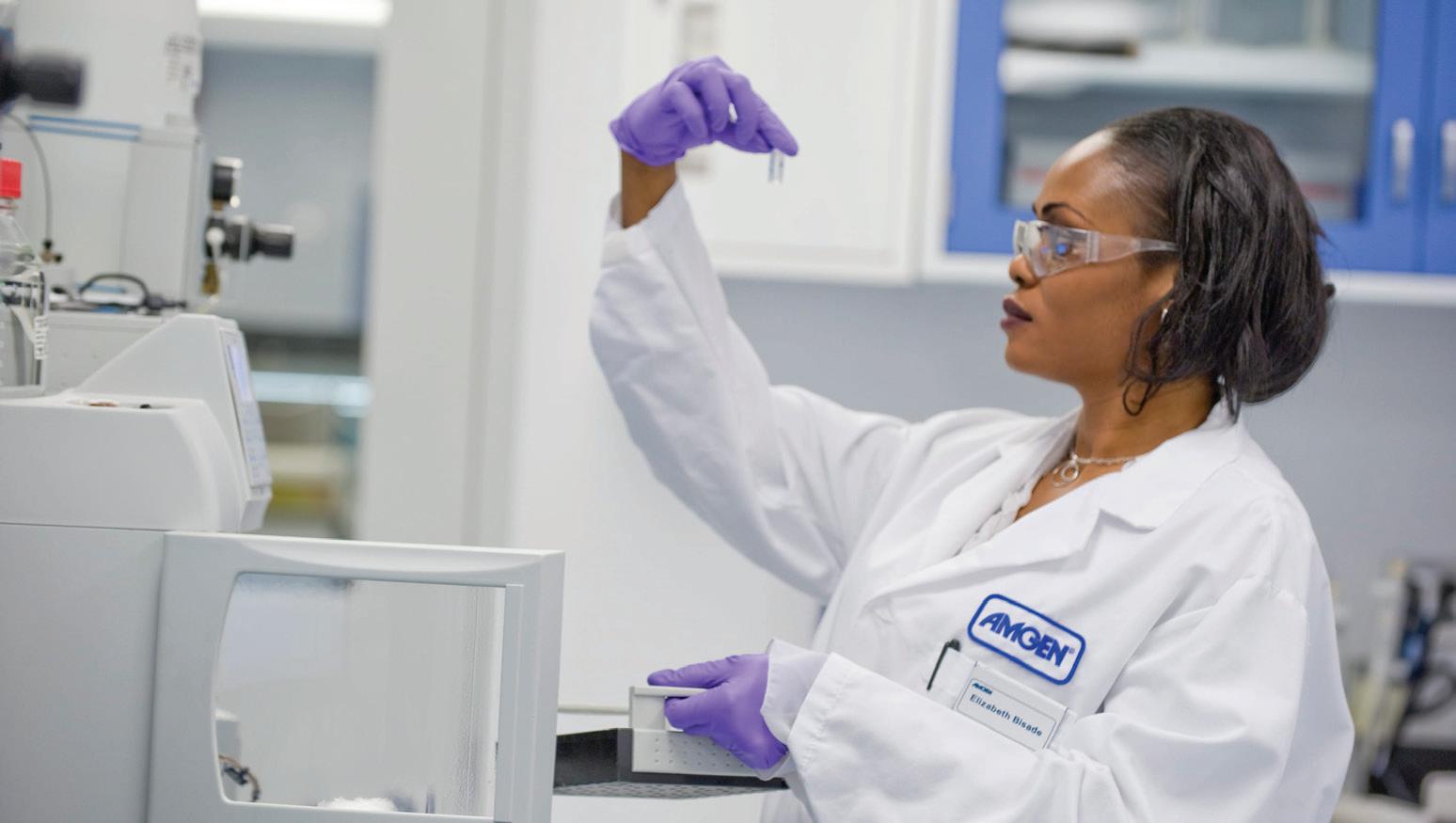
Companies like Amgen, recently named one of the World’s 25 Best Workplaces by Fortune, are leading the way and tackling some of healthcare’s most complex digital automation technologies. With brands like Enbrel and Otezla and a worldwide presence, Amgen responded to a growing demand for human therapeutics by establishing a 270,000-square foot facility near Columbus and building on the city’s collaborative and innovative global healthcare supply chain network.
JobsOhio added the military and federal installations as the No. 10 target sector in 2018. It has positioned Wright-Patterson Air Force Base as a prime beneficiary of federal base closings, relocations, and expansions.
In September 2021, the U.S. Air Force chose the 179th Airlift Wing at MansfieldLahm Airport to host the Air National Guard’s Information Cyber Warfare Wing. This new mission will bring more than $50 million in capital investments to Richland County and position Ohio on the front lines of the military’s fight against cyber threats.
Aware, located in Columbus and one of the leading enterprise-grade collaboration governance platforms specializing in human behavioral data, recently finished a $60 million Series C funding round less than one
year after JobsOhio Growth Capital Fund, Ohio Innovation Fund, and other capital venture partners contributed to its Series B equity investment. As one of the many tech startups accelerated by the JobsOhio Growth Capital Fund, Aware expanded its capabilities in addressing data risks and insider threat concerns related to critical online messaging and collaboration tools.
In addition, Ohio continues to play a crucial role in developing Advanced Air Mobility technologies with robust supply chains, test markets, partners, and legislation that both public and private sector entities can rely on. Ohio lawmakers have opened the skies for Unmanned Aircraft Systems Traffic Management (UTM) and Urban Air Mobility (UAM). In August 2022, JobsOhio and 15 other AccelerateOhio partners broke ground on the National Advanced Air Mobility Center of Excellence in Springfield, Ohio, which will serve as the physical space for the collaboration, pushing the speed and depth of the partnership to research, design, and test deployment. &
The R&D Center Grant Program helps support targeted industries, including Advanced Manufacturing, Aerospace & Aviation, Automotive, Healthcare, Financial Services, Food Processing, Information Technology, Logistics & Distribution, and Shale Energy & Petrochemicals.
Project factors that determine grant eligibility include:
• Alignment with JobsOhio sector strategies
• Job creation
• New payroll
• Fixed-asset investment commitments
• Project location
• Applicant’s track record in successful R&D commercialization
Eligible uses of funds include:
• Industry-driven, value-added applied research
• Software development
• Developing technologies that a corporation can commercialize
To learn more about the grant program and other JobsOhio initiatives, visit the website: www.jobsohio.com.
Institute of Nuclear

Research
https://en.iner.gov.tw
Nuclear safety and nuclear back-end Radiation applications for people’s livelihood Green energy and system integration


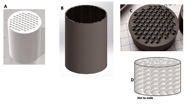
In Taiwan, the diesel burner drying technique is generally employed to dry the garlic and many issues are caused such as time and energy consumption, noise and environmental pollution. The solid desiccant wheel dehumidification system is applied to remove parts of moistu re content from garlic for better storage stability, shortening drying time, energy saving, minimizing drying process noise and air pollution contamin ant emission. The solid desiccant wheel is manufactured using activated alumina derived from aluminum dross with a three-dimensional random porous stru cture and applied to adsorb moisture from the garlic. The equilibrium time for the solid desiccant wheels and humidity is determined by observed kinetics in the adsorption kinetic experiment. The adsorption capacity of solid desiccant wheel with different porosity ranging from 20 to 60 pores p er inch (PPI) is a function of time at 25°C and 30% relative humidity. The adsorption equilibrium time of desiccant wheel (60 PPI) with 150 mm diameter and 50 mm thickness is twelve minutes. The maximum adsorption capacity is 61.2 g (12 minutes) and per gram of desiccant wheel can adsorb 0.24 g wat er. The desiccant wheel is divided into two working areas e.g., adsorption and desorption. As the adsorption capability of desiccant wheel is sat urated, the wheel is rotated to regeneration area to remove water by heat. The maximum adsorption capacity of desiccant wheel per hour can be reached at 306 g. A trial run of a solid desiccant wheel (diameter 500 mm, height 200 mm) dehumidification system to dry garlic with the capacity of 4,000 kg is executed, 30% of water from the garlics is removed in the period of 14 days and the operation time is 10 days shorter than the traditional diesel burner drying process. The noise and air pollution derived from the diesel burner drying process can be avoided.
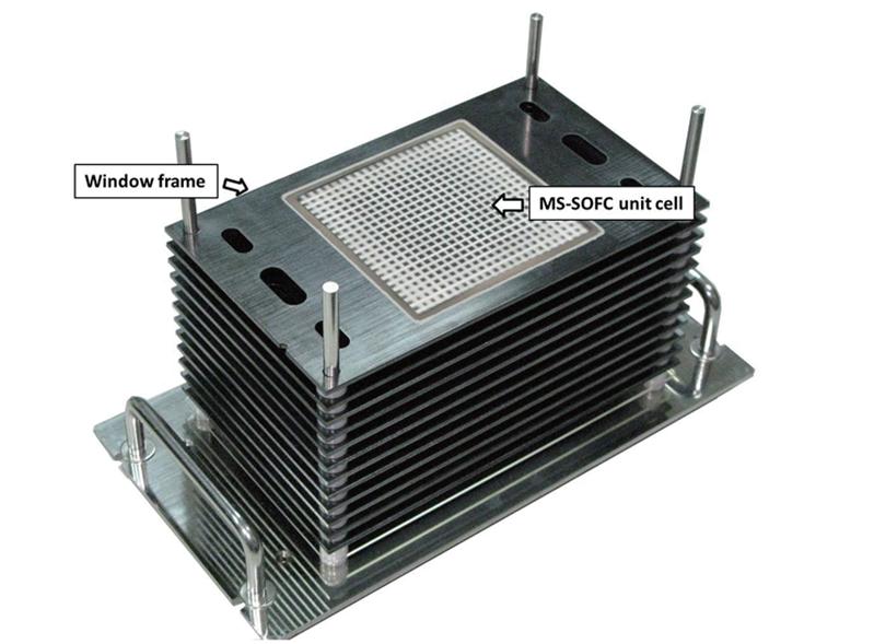
INER (Institute of Nuclear Energy Research) had devoted to the development and applications of the solid oxide fuel cell (SOFC) power generating technology. A fabrication cluster, named sofciner-MS, for cell unit of solid oxide fuel cell by atmospheric plasma spray-sintering on metallic substrate for high structural durability and fast warm up is developed. From powder to power, we establish a production procedure to manufacture Sofciner-MS cell units by many industry techniques. INER’s proprietary atmospheric-plasma-spray-sintering technique allows SOFC to overcome its traditional problems in structural and thermal strengths. Now, at 0.9V and 650, 600 and 550°C, the power outputs of 10 10 cm 2 Sofciner-MS cell unit can reach 34.8, 26.7 and 16.5W, respectively. The maximum power outputs at 0.7V and 650, 600 and 550°C might reach 70.8, 48.8 and 28.8W,

respectively. The degradation rate of Sofciner-MS cell unit is less than 3%/khr. INER aims to be a strong technical support to the industry and promote the commercial production of SOFC in Taiwan. SOFC contributes importantly to energy use. Sofciner-MS makes SOFC realistically more practical for real-world applications like transportation.


Plasma-sprayed metal-supported solid oxide fuel cell


st, a t 97.5% and Si-PV with more


Micro-CPV module developed by INER with fully automotive fabrication process.

Since 2003, The Institute of Nuclear Energy Research (INER) has developed High-concentration Photovoltaic (HCPV) system technologies, including III-V solar cell epitaxial and processing, concentration module processing, solar tracking device, system integration, control and monitoring, and module qualification. Concentration photovoltaic (CPV) system is a photovoltaic system utilizing an optical system to concentrate sunlight onto a small solar cell to reduce the consumption of expensive solar cells. Now, INER has successfully developed micro-CPV technology with a fully automotive fabrication process. The conversion efficiency of INER’s micro-CPV module is 35.5%.Field performance test of INER’s micro-CPV system and commercial Si-PV system is demonstrated in Taiwan. According to the sunlight exposure test, the micro-CPV system maintained a high energy yield at 97.5% and Si-PV system dramatically decreased to 83% with the increase in solar radiation intensity.The micro-CPV system provide high energy yield, i.e., provides more electric power in a high solar irradiance area.

and Advanced Materials Institute

Oak Ridge National
Park
Pfeiffer
Pittcon
Alamos
Mike Emich 508.446.1823 memich@wtwhmedia.com @wtwh_memic

Matheson 805.895.3609 mmatheson@wtwhmedia.com @mmatheson
Brownlee


