8 minute read
Semicon market screams for innovation in chip testing
When testing their chips, semiconductor manufacturers have to fi nd a balance between developing their own equipment and purchasing solutions. Those who lead the way are faced with diffi cult choices. Innovation is the message, as demonstrated by the Salland Engineering test symposium.
René Raaijmakers
Advertisement
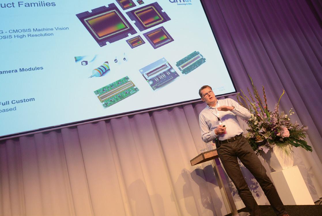
“I ’d like to challenge the vendors of automated test equipment who are here.” Peter Crabbe, director of operations at Austriamicrosystems (AMS) Sensor Belgium, took a provocative stance at a recent symposium for IC testing, organized by Salland Engineering in Zwolle. Crabbe told the test technology vendors present that AMS Sensor from Antwerp is still testing 80 percent of its image sensors with its own equipment. is is partly for historical reasons. Cmosis, incorporated by the Austrians in 2015 and now part of their sensor division, developed all its test systems itself.
While many chip manufacturers are moving their testing activities to Asia, where they’re much cheaper to perform, AMS continues to test its image chips in Europe. “To a large extent, we do this to protect our knowledge,” says Crabbe. “Also, manufacturing a test system yourself is still signi cantly cheaper than buying one from an ATE supplier,” he confronted his audience, which consisted largely of manufacturers of test equipment. He challenged them to innovate more.
But Crabbe does see the advantages of purchasing equipment. “Because of the way ATE manufacturers feed the information back, chip designers can learn a lot more.” Instruments made in-house usually focus on only one thing, namely, to decide whether or not a chip is good. Commercial ATE testers, on the other hand, are heavy computers that extract large amounts of information from chips via their bonding pads. is allows for much more than just selecting between good and bad. Improving designs is an advantage, but with good
1.7 billion AI engine startup Graphcore plugs into Dutch test technology
tests, it’s also possible to identify ‘secondchoice’ samples. It’s expected that the ATE industry will make great strides in the near future based on this data in combination with machine learning techniques and advanced algorithms.
Crabbe, a former COO of Salland in Zwolle, at the end of his presentation: “When we buy test equipment, we always want to be able to fall back on instruments we’ve developed ourselves. After all, the imaging market is very innovation driven. We’re constantly pushing back frontiers and we have no guarantees that we’ll be able to buy the necessary test technology o the shelf.”
“You always have to make a careful consideration,” explains Paul van Ulsen, director of Salland Engineering and organizer of the test symposium. “Developing IC tests is simply quite expensive. However, some tests have to be developed by chip manufacturers themselves, because the market simply doesn’t o er anything yet.” Van Ulsen sees Crabbe’s comments mainly as a call to test suppliers to come up with new solutions more quickly. “ at’s also why we’re organizing this symposium. To bring the whole chain together: from design to chip production to test instruments and their users.”
With Salland Engineering, the Netherlands now has a good position in the testing world. Van Ulsen: “ e fundamental testing technologies we develop are used by various chip manufacturers and ATE suppliers.” With state-of-the-art test hardware and software, the Zwolle-based company serves 95 percent of the global ATE manufacturers.
Biggest chip
It comes as no surprise that as the complexity of the components increases, the testing costs go up as well. Paul Elford of UK-based
Paul Elford, Graphcore: “We have a data management problem instead of a straight test problem.”
Graphcore presented an extreme example of this at the test symposium. Graphcore recently received 200 million dollars in additional funding from investors including BMW and Microsoft. is brought the 3-year-old company to a total funding of 300 million dollars and an estimated value of 1.7 billion dollars. Graphcore develops chips for applications ranging from identifying cancer to helping online media to gure out which adverts to send to you. e Graphcore chip is a parallel array of 1,280 processors, each with a computing power of 100 giga ops. is so-called “intelligence processing unit” (IPU), is made up of 26 billion logic transistors and 2.6 billion memory bits. e IPU is actually the biggest die that foundries can produce in one lithographic exposure. “We went to TSMC and asked what the biggest chip would be they could produce. eir response was 25 by 32 millimeters. We took that size and crammed it with everything we could. Given that size, there are only 66 dies in a wafer,” Elford explains. e chip broke records when it was produced last year. “If you look up Moore’s Law on Wikipedia, you’ll see a timeline with all kinds of processors,” Elford says. “You’ll nd our GC2 IPU in the top right of the graph,” he proudly adds.
In the test process, all 85,000 processors on a wafer are probed. A certain degree of redundancy ensures that not all cores have to be functioning. Even a die with four defect cores will still work. Five probe tests yield about 19,000 test results per die. Elford: “We have to store this data to compare it to other stages in the test program. Actually, we have a data management problem instead of a straight test problem. We’re constantly gathering, comparing and making decisions: can I repair this chip, or does it have to go in the bin?” e data also helps to improve yield. “We have 10 percent loss on a wafer, and we feed that back to TSMC. If we show them the patterns with hot spots, they can build a much better picture of what happened on the die and they can improve their process. ey’re able to see error patterns that they never would have seen if we just reported some dies failing.”
AMD, Intel and Nvidia
Elford, who’s in charge of production test outsourcing, explains the problem that Graphcore has with scale. “To connect all these processors, we have exchange blocks that enable any of the 1,280 processors to talk to any other processor on the chip.” To take care of o -chip communication, the IPU has twelve 8 Gb/s Serdes ports to talk with any other processor in a system.
Graphcore actually doesn’t sell its IPUs as components but produces line cards with two of these processors. Computer makers like Dell use the building blocks to make cloud servers. Elford: “ e cards speak to
Peter Crabbe, AMS: “We always want to be able to fall back on instruments we’ve developed ourselves.”

any other line card in the system and in this way, you can quickly build up a huge amount of processing power.”
While competitors like AMD, Intel and Nvidia have lots of experience and knowledge in-house, Graphcore concentrates on its core technology and relies heavily on its network of suppliers. “We use some of the best technology suppliers in the world: TSMC for production, ASE for packaging and Teradyne for ATE testers,” Elford states. “Each of them helps us in one speci c area.” Salland Engineering has developed the hardware and software for a test interface card with 7,000+ probe needles to check over 27,000 bumps that are available on the UPI for I/O and power.
“We coordinate and keep the global view,” Elford explains his role. “However, it’s not quite that easy. is is a very demanding industry and we’re stumbling upon quite some engineering problems.” As an example, he mentions the problems that arise with short-circuiting. “ is is a standard issue, but where do you start? We’re the coordinator for everything, so we have to go to every subcon to gure out where the problem is: the card, the tester, the test hardware, the silicon, the package – or does something just need a cleaning?”
As an example of the test challenges, Elford shows what can happen when following a procedure that’s quite standard in the market. “If we want to stress the chip, applying a high supply voltage is an easy thing to do. But to raise the supply voltage to 1.5 times the average, the heat that’s generated can quite quickly result in a meltdown.”
Optical techniques
New frontiers were also touched upon in Zwolle. Just as AMS needs light to test its image sensors, so will special optical technology have to be developed to validate components with integrated photonics. “Everyone talks about it, but a lot is still unclear,” says Van Ulsen. “How are we going to handle and measure it in high volume?”
At Salland’s test symposium, German Ficontec and Taiwanese Chroma ATE showed that they’re now applying optical techniques in practice. Chroma talked about test experiences with diode lasers, Ficontec discussed the development of machines and precision technology for photonic chips. The challenge there is to achieve a high throughput. While probe cards for electrical testing may contain thousands of contacts, high-throughput test systems do not yet exist. The German company already makes systems in which a few laser beams touch optical chips, but scaling up to tens or hundreds of beams still has a way to go. Ficontec’s Stefan Schlörholz: “It’s not just a challenge to find the probe surfaces we need to irradiate but also the points where we need to read the signals.”
7 OCTOBER 2020 IGLUU EINDHOVEN


Platinum sponsor
Sponsors


Partner
Powered by


