7 minute read
Multibeam SEM shifts 3D cell imaging into top gear
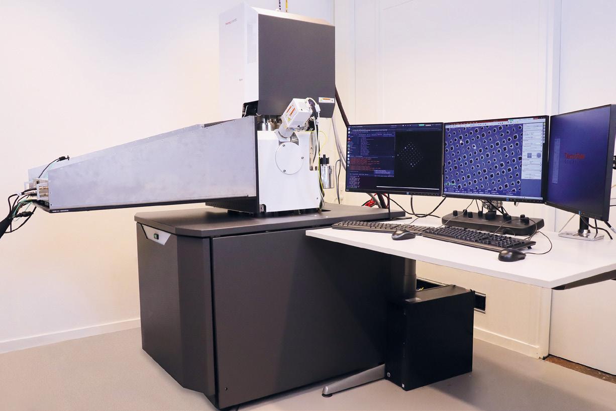
Medical and biological scientists are eager to create 3D images for their research at nanometer resolution. However, without an efficient technique to make the scans, the process is difficult and painfully slow. To make this research feasible, Delft University of Technology is teaming up with a consortium of enterprises to develop an innovative device: a multibeam scanning electron microscope.
Antoinette Brugman
Advertisement
Making a detailed 3D image of cells or tissues is very interesting for research in life science domains like cell biology and medical tissue biology. This would provide researchers with both an overview of tissues and detailed information on a nanoscale. Creating such 3D images requires taking very thin slices of the cell structures or tissues and then scanning them in order to build a 3D reconstruction.
This method requires a device that’s able to scan each slice separately and in detail. Until now, this device was the difficult part. A ‘normal’ light microscope can produce a picture of the sample directly. However, with a maximum resolution of only about 400 nm, it’s just not detailed enough. With a resolution of about 1 nm, a traditional scanning electron microscope (SEM) does provide sufficient detail; however, scan
ning all slices pixel-by-pixel would take months or years to complete.
User friendly
Thinking there had to be a better way, a group of Dutch organizations, including Delmic, Technolution and Thermo Fisher, joined forces with Delft University of Technology (TU Delft) to establish a consortium to create a new type of SEM – a multibeam SEM. The aim of their endeavor was to build an innovative device with a high resolution and a strongly increased throughput, in order to speed up the scanning process and bring measurement times down to days or even hours. Features that make the multibeam SEM a suitable large-volume technique for research in the life-sciences domain.
“We were aiming to develop a device that would be a hundred times faster than the traditional SEM and with a very high resolution,” says Andries Effting, CTO at Delmic. “At the same time, we wanted to develop a user-friendly system that would be able to run with minimal user input – more or less, working independently. Last, but not least, we wanted to achieve this at a reasonable cost for our customers.”
Since the consortium started two years ago, the partners have made a lot of progress. Together, they’ve built an alpha and a beta system. These systems provided proof-of-principle and were necessary steps to see whether there were no design faults in the engineering part. At the moment, collaborators are working on the final design of the multibeam SEM – a fast, user-friendly device with a resolution of 4 nm – to be launched at the end of this year.
Each consortium member brings in its own specialties. At TU Delft, researchers have already been working on a multibeam SEM technique for over ten years. Currently, a series of PhD students are doing research to make the multibeam system usable.
Image of a rat pancreas section. Sample courtesy of Ben Giepmans, Cell Biology University Medical Imaging Centre UMC Groningen
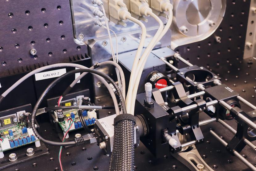
With its host of knowledge and experience in building SEMs, Thermo Fisher provides the infrastructure for the new device. Technolution mainly focuses on the sensors and the data acquisition and processing. It’s responsible for the entire data stream, from reading out the data, to image processing and data storage. Delmic is taking care of sample handling, detector optics and software integration of the system, as well as being concerned with selling the product to customers.
64 CRT TV screens
A SEM produces images of a sample by scanning the surface with a focused beam of electrons. The electrons in this beam interact with the sample in a variety of ways, resulting in three different populations that can be detected. In a traditional SEM, two of these are usually measured with detectors mounted above the sample: the secondary electrons, which provide information about surface features, and the backscattered electrons, which provide information about the composition of the material.
The third population can be detected in a setup known as a scanning transmission electron microscope (STEM). In such a device, a detector underneath the sample identifies electrons that pass through. For the imaging of biological samples, the transmitted electrons provide valuable information, as they enable visualization of local differences in densities inside the sample.
A STEM detects both the amount and the energy of the electrons passing through the sample, thereby providing information about the local density. The number of electrons passing through depends on the sample’s structure. The denser the material, the more electrons are scattered and do not reach the STEM de

tector. This results in a lower intensity of the transmitted electron beam. Scanning the sample pixel-by-pixel produces an image that shows the local density differences of the tissue structures. As life-science researchers are particularly interested in imaging cell membranes, they stain these membranes to enhance the contrast in their samples.
Marc van Eert, an applied scientist at Technolution, explains: “Normally, a STEM uses only one electron beam. We’ve developed one with several beams, scanning different parts of the sample at the same time. This is possible because, in transmission mode, the secondary electron beams can be measured separately. Our device is designed with a grid of eight beams by eight beams, so 64 in total. This speeds up the process enormously. You can compare our system with 64 CRT TV screens writing their images at the same time and each showing one section of the bigger picture. However, in our case, we’re not writing an image but reading a sample with 64 electron beams at the same time. Each beam scans a different part of the sample – an area of 3.2 µm by 3.2 µm. Subsequently, the information of all 64 separate beams is combined to compose one image out of it.”
Imaging on demand
Although this sounds rather easy, there were many technical challenges in designing the new device. “We couldn’t realize this kind of system in an evolutionary manner – by doing some incremental changes – because we needed to adapt all parts of the system at the same time to convert it into a multibeam machine,” explains Van Eert. “This wouldn’t have been possible without using systems engineering. In fact, we reshuffled the existing SEM system completely and brought it to a new operational principle. So, we worked on it in a more revolutionary way. As a result, we also managed to design a system with a shorter dwell time per pixel – the exposure time needed for the electron beam to scan one pixel of the sample. This also speeds up the process substantially.”
Working with many electron beams at the same time brings two obvious challenges: limiting crosstalk between adjacent beams and finding a smart way of using all beams to compose one picture that covers the whole sample surface. As the electron beams operate very closely to each other, one beam signal may influence neighboring signals. This crosstalk effect had to be minimized, to get the right information from all individual

The system has been completely reshuffled and brought to a new operational principle.
Credit: multibeam SEM consortium
beams. The partners have achieved this by very accurately aligning the beam optics with the detector. During the acquisition process, the alignment is continuously monitored and adjusted when necessary.
Composing one image with information derived from all 64 electron beams requires each beam to scan its own area, including some pixels of neighboring beams. This overlap is necessary to get a complete picture out of all beam signals and thus to be sure no information is missing. By calibrating the system, it’s possible to determine how the different images should be composed to make one image out of them.
“In fact, the whole concept has changed compared to a traditional SEM,” Van Eert clarifies. “As scanning with a traditional SEM is rather time consuming, the researcher needs to operate the device himself to carefully select the specific part of the sample he’s interested in. Because the multibeam SEM enables scanning of a large area independently and in a reasonable amount of time, it’s possible to do the whole sample at once and make a smaller selection of this area later. The multibeam SEM can thus be used by a technical operator, who just facilitates scanning of the samples and delivers the image data to the specialist. This way of operating even opens the door to realizing scan centers, which – just like copy centers delivering copies to their customers – carry out imaging on demand.”
Another challenge is the sheer amount of data the system produces, Effting adds. “We’ve made a roadmap towards a data acquisition rate of one gigabyte per second, which means a full hard disk drive every two hours. Imagine running the system 24/7 for a couple of weeks. This will produce a huge amount of data. Moreover, all this data has to be processed. On top of all this, we have to make sure that the researchers preparing the samples can keep up with the machine.”


