
23 minute read
Taking off might have been the easy part for CITC
The Chip Integration Technology Center (CITC) plane has taken off, but there are a lot more seats to fill. ‘Captain’ Barry Peet explains how he intends to do so.
Paul van Gerven
Advertisement
The initial team has been assembled, the lab space is filling up with tools, experiments are being conducted and Fieldlab status has been awarded: the Chip Integration Technology Center (CITC) at the Novio Tech Campus in Nijmegen is up and running. There even was an opportunity to celebrate the occasion. On 5 March, four days before the Dutch people stopped shaking hands, a crowd of industry executives and government officials gathered to see the proverbial ribbon cut.
The event must have felt like a bit of a personal victory for Barry Peet, who as managing director of the Business Cluster Semiconductors (now called Holland Semiconductors) put a lot of effort into getting the open-innovation center off the ground. After getting companies, governments and partner institutes on board, Peet now gets to head up CITC.
A little over a week after the event, however, Peet is primarily interested in looking towards the future – he has to, he explains, because his mission is far from over. “I’m happy with our expeditious start, but I consider CITC still to be a startup. Over the next few years, it’s imperative that we attract additional customers, broaden our scope and, above all, prove we have something to contribute,” says the managing director.
World-class player
CITC focuses on the final stages of the chip manufacturing process, referred to as the back-end. Traditionally, this involves wrapping freshly baked chips with a protective wrapper while also taking care of the electrical connections to the outside world. Though a crucial part of making a functional chip, these processes have lived a life in the shadows for a long time. Cutting-edge lithography or the black arts of material composition and deposition – such frontend issues catch the imagination.
Semicon hotspot Nijmegen
“Nijmegen is evolving more and more into a substantial health and high tech hotspot. It’s one of the places to be as a semiconductor company. The open technological innovation center CITC is, therefore, a welcome and valuable addition to the city and will amongst others be working on technological innovations that contribute to worldwide connectivity and health,” explains Rikus Wolbers, program manager of Briskr, the consortium of organizations that supports health and high-tech companies in the Nijmegen region.
Over the past decade, however, the interest in – and glamour of – packaging has been growing rapidly, for a variety of reasons. One of them is simply the advance of semiconductor technology in general. As elements within a chip kept shrinking and its functionality expanding, chipmakers ran out of room for the electrical connections. New packaging techniques were required to make them fit.
Another reason is size: smartphone manufacturers want to keep making their products better but not bulkier and more power hungry. Naked chips are generally as small as they can get, so packaging has to step up. For example, multiple chips can be combined – or integrated – in a single package, thus reducing size, as well as overall power consumption. This isn’t just of interest to smartphone manufacturers; many applications stand to benefit from such advanced integration. The Internet of Things will never happen without it.
Emerging applications, in general, drive the need for new or better-performing semiconductor technology. Th e range of an electric car partly depends on the performance of the power electronics on board, and the performance of those chips partly depends on their packaging. Th is is also the case in the RF (wireless) domain, for example in 5G’s rollout.
A complete list of advanced packaging and integration technologies would fi ll many pages, and CITC will cover only a few of them. “It would be impossible to cover the entire back-end and become a worldclass player. We need to focus,” explains Peet. “Besides, we don’t want to compete with any existing activities. Imec, for example, also has advanced packaging programs. It would make no sense to start competing with those.”
Imec does serve as CITC’s inspiration, in terms of both the status the Leuven institute has achieved in the semiconductor industry and its business model. Th e Nijmegen center, too, will be working with companies, universities and research institutes to bridge the gap between basic research and corporate R&D. Any technology CITC develops, will be shared among participants.
CITC launched with three customers onboard: Ampleon, Nexperia and NXP. Your programs in the packaging of highpower and RF electronics appear to be neatly tailored to their needs. Isn’t that a rather narrow focus?
Peet: “We needed a couple of large customers to get going. Next, we need to attract more companies. Eventually, we want to
Four packaging technologies and two additional missions the CITC focuses on (or intends to focus on in the near future). Credit: CITC


cover the whole value chain, so we’re reaching out to material suppliers and equipment manufacturers, for example. Based on whatever needs and opportunities arise along the way, we’ll expand our programs. It’s a step-by-step process.”
Do these prospective customers include SMEs?
“Absolutely, this is a high priority. But fi rst, we have to fi nd the right proposition for SMEs. Clearly, no SME will join a four-year program that costs 50-100k per year. We might be able to help out smaller companies with specifi c, well-defi ned issues. We’re considering voucher arrangements, for example, to make that happen.”
at sounds a lot like you’ll be providing services. Shouldn’t that be left to commercial parties?
“We need to be very careful about that. First of all, we might become too dependent on the fees, which is a risk. Secondly, we don’t want to compete with existing companies. On the contrary, whenever a company has a service available that CITC needs, we’ll cooperate with that company.”

An SME packaging company, Sencio, is located literally one hundred meters from CITC, yet it’s not involved. Why not?
“I really would like to have Sencio onboard, it’s a matter of fi nding a way that works for us both. Surely having an advanced packaging research institute in its backyard is an advantage for a company like Sencio. For example, we could develop technology together for a customer with special requirements, where they can take care of volume production.”
Sencio, is located literally one hundred meters from CITC, yet it’s not involved. Why not?
“I really would like to have Sencio onboard, it’s a matter of fi nding a way that works for us both. Surely having an advanced pack
Past experiences have shown that open-innovation institutes struggle to be of relevance for SMEs. In the end, they need the deep pockets of large companies, often from abroad. Will it be di erent with CITC?
“I don’t think we can afford to sidestep world-class players if we want to become world-class ourselves. And, indeed, in our line of business, these players are in Asia.”
If that’s the case, aren’t you running the risk of developing technology that’s subsidized by the Dutch taxpayer but primarily monetized abroad?
“Our mission is to make sure everyone involved reaps the rewards from the collaborative eff ort. I’m aware who’s funding us, and what’s expected in return. I strongly believe CITC can deliver because of the opportunities that collective R&D activities provide. I don’t mind becoming an R&D vehicle for a company, as long as additional parties stand to gain from our work.”
Some of the subsidies that were provided to start CITC are a one-time deal. As time passes, you will be expected to get by on less public nancing. How will you manage?
“I’m optimistic about finding funding, because our government, as well as the European Union, are increasingly emphasizing the importance of Key Enabling Technologies. We should be able to draw upon those funds.”
More customers, relevancy for SMEs without competing with them and funding: clearly, Peet wasn’t exaggerating. He’ll need to shake a lot more hands over the next few years.
From a cryogenic CMOS controller for quantum computers to an ultra-low-power transceiver for ingestible electronics pills – our small corner of the globe again came up with a lot of top-notch IC design.
Paul van Gerven
The International Solid-State Circuit Conference (ISSCC) is a mecca for the international IC design community – both from academia and industry. Getting a paper accepted is the highest honor that can be bestowed on an chip designer. is year’s edition, held 16-20 February in San Francisco, featured eight papers from researchers working at Dutch universities (seven from Delft and one from Twente), one from NXP (and another one in collaboration with Delft) and ve from Imec (including Imec Netherlands, which participates in Holst Centre).
We asked the honorees about their work. NXP, unfortunately, was unable to contribute.
Delft University of Technology
e world’s rst cryo-CMOS controller for spin and superconducting qubits
Paper: A scalable cryo-CMOS 2-to-20 GHz digitally intensive controller for 4×32 frequency multiplexed spin qubits/transmons in 22nm FinFET technology for quantum computers Researchers: Bishnu Patra, Jeroen van Dijk, Edoardo Charbon, Fabio Sebastiano and Masoud Babaie Collaborators: EPFL, Intel, TNO
What is your paper about? What did you design?
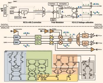
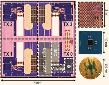
e paper proposes Horse Ridge, the rst cryo-CMOS controller IC for spin and superconducting qubits, the core computational units of quantum computers. Cryo-CMOS means that the CMOS IC operates at cryogenic temperatures, in this case 3 kelvin (-270 degrees Celsius). is means that the controller can be placed inside the cryogenic vessel of the quantum computer where the qubits reside. is in turn enables unprecedented levels of miniaturization, paving the way for scalable architectures that can handle larger and larger number of qubits – which are required to make quantum computers practical.
What applications could it be used for?
All quantum devices requiring a very precise arbitrary waveform with gigahertz frequencies and extremely precise phase and amplitude control can bene t from Horse Ridge. Quantum computing is the main application, obviously, but new applications in quantum communications and quantum sensing are also expected to emerge.
Why is it superior to previous designs?
is design achieves a much larger number of channels than previously achieved, ie it can control many more qubits simultaneously. In addition, Horse Ridge has a very sophisticated way of suppressing interference between qubit controls, thereby allowing for more reliable control of a larger number of qubits. Finally, the chip has a rich micro-instruction set, thus enabling easy programming of qubit operations from a higher level of the quantum stack.
Why is this contribution ISSCC worthy?
It was selected because of the compelling architecture based on digitally-intensive design with a clear roadmap for extension in the near to medium term to achieve scalable quantum computers thanks to localized qubit control at cryogenic temperatures. In addition, the performance of the chip and its design for use at 3 K was a strong argument in favor of presenting the work at the conference in an all-quantum session. is trend, with a second keynote speech on quantum computing in three years, attests to the growing interest of the solid-state IC community in quantumrelated problems.
A most versatile cryogenic oscillator
Paper: A 200 dB FoM 4-to-5 GHz cryogenic oscillator with an automatic common-mode resonance calibration for quantum computing applications Researchers: Jiang Gong, Masoud Babaie, Fabio Sebastiano, Edoardo Charbon Collaborators: EPFL, Intel
What is your paper about? What did you design?
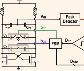
We proposed a digital calibration loop that automatically adjusts the oscillator common- mode resonance at twice the oscillation frequency to ensure that the oscillator always operates near its optimum performance. is technique suppresses the oscillator phase noise at 100 kHz o set frequency by more than 10 dB over the temperature range from 4-300 K.
What applications could it be used for?
e proposed calibration is a general technique to reduce the oscillator phase noise. Consequently, its applications are broad, ranging from wireless communications to quantum computing, where low-power and high-accuracy frequency generation is required.

Why is it superior to previous designs?
Our design simultaneously achieves lower phase noise and lower power consumption compared with the state of the art. It’s enabled by a digital calibration technique, which ensures that the oscillator’s capacitor con guration is optimal. Furthermore, the proposed circuit dramatically reduces the design costs and time-to-market since any o -chip factory-level calibration is avoided.
Why is this contribution ISSCC worthy?
is work will enable the realization of cryogenic low-power low-jitter frequency synthesizers required for the control and read-out of quantum bits. Additionally, RF oscillators are the heart of any communication system. Our digital calibration automatically adjusts the oscillator con guration such that the oscillator operates near its optimum performance across di erent process, voltage and temperature variations.
An RC frequency reference with quartz-like accuracy
Paper: A 16 MHz CMOS RC frequency reference with ±400 ppm inaccuracy from -45 °C to 85 °C after digital linear temperature compensation Presenters, group leader: Cagri Gurleyuk and Sining Pan, Ko Makinwa Collaborator: In neon
What is your paper about? What did you design?
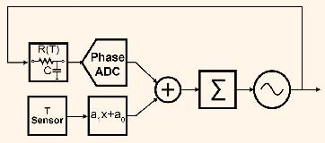
Our paper describes a CMOS frequency reference that achieves high accuracy about 400 ppm around its nominal 16 MHz output frequency after an industrially feasible two-temperature trim. Since most of the remaining error is systematic, this can be reduced to below 100 ppm with the help of a one-time batch calibration. e frequency reference works by locking an inaccurate ring oscillator to the well-de ned time constant of an RC lter. A high-resolution resistor-based temperature sensor then compensates for the lter’s residual temperature dependence.
What applications could it be used for?
All communication standards require a frequency reference. Our work allows wired communication standards such as CAN or LIN to be fully realized in a system-onchip, obviating the need for external quartz or MEMS oscillators. is is industrially attractive because it reduces component count and board area, thus reducing manufacturing cost.
Why is it superior to previous designs?
It achieves best-in-class accuracy, over a statistically relevant number of samples and over multiple batches. Also, while previous designs relied on expensive multitemperature calibration, our work only requires a simple two-point calibration, which can be combined with a one-time batch calibration if more accuracy is required.
Why is this contribution ISSCC worthy?
Our design achieves the best reported accuracy for an RC-based frequency reference and as such, it will be a benchmark for future designs. It’s also the rst one that does this with an industrially feasible calibration methodology and with low area and power dissipation.
An ampli er for better ultrasound images of the heart
Paper: A 2 pA/√Hz transimpedance ampli er for miniature ultrasound probes with 36 dB continuous time-gain compensation Presenters, group leader: Eunchul Kang and Mingliang Tan, Michiel Pertijs Collaborator: Vermon
What is your paper about? What did you design?
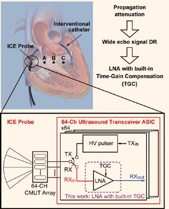
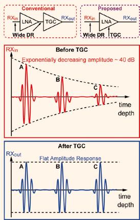
Our paper describes a low-noise ampli er of which the gain can be smoothly varied over a 40 dB range. e ampli er is designed for integration in a miniature ultrasound probe, in which it’s responsible for amplifying the received echo signals from which the ultrasound images are reconstructed. It compensates for the decaying amplitude of the received echoes with time, thus saving substantial power by relaxing the dynamic range requirements of the rest of the receive chain.
What applications could it be used for?
Our design is intended for use in miniature ultrasound probes, such as intra-cardiac imaging catheters, in which many tiny transducer elements emit sound waves and receive echo signals to make a real-time image of the body. Together with our collaborators from Vermon, a leading manufacturer of ultrasound probes, we incorporated the new ampli er into a prototype of a 64-element intra-cardiac imaging probe.
Why is it superior to previous designs?
e presented ampli er is unique in that it provides continuous smooth gain control, leading to improved image quality compared to earlier designs that use discrete gain steps. With a chip area of only 0.12 mm 2 , the presented ampli er is small enough to be integrated directly underneath a transducer element. e realized functionality was previously only available in ampli ers used in ultrasound imaging systems, which are too large to be integrated in a miniature probe and consume far more power. Our low consumption of about 5 mW per ampli er is crucial in probes that operate within the human body, since their power consumption needs to be minimized to avoid overheating.
Why is this contribution ISSCC worthy?
e presented ampli er employs a new circuit topology consisting of a capacitive ladder feedback network and a current-steering circuit to obtain an accurate linear-in-dB variable gain. It’s the rst time that this functionality is reported in a design that’s suitable for integration into a miniature probe. We’ve integrated the ampli er in a 64-channel ultrasound transceiver ASIC and combined this with a CMUT transducer array in a prototype catheter-based intra-cardiac probe. B-mode images of a tissue-mimicking phantom are presented that show the bene ts of the ampli er scheme.
University of Twente
An IoT design Don Quixote wouldn’t be able to resist
Paper: A 370 µW 5.5 dB-NF BLE/BT5.0/ IEEE 802.15.4-compliant receiver with >63 dB adjacent channel rejection at >2 channels o set in 22nm FDSOI Researchers: Bart ijssen, Eric Klumperink, Philip Quinlan, Bram Nauta Collaborator: Analog Devices
What is your paper about? What did you design?
We presented a 2.4 GHz multi-standard Internet-of- ings (IoT) wireless receiver fabricated in 22nm FDSOI. e receiver can be used for multiple IoT applications such as Bluetooth Low Energy (BLE) and Zigbee. In addition to careful design across the entire receive chain, we included two main innovations: an analog nite-impulseresponse (FIR) lter and a novel frequency divider architecture. e analog FIR lter acts as channel selection lter and improves the receiver’s blocker resilience. is analog implementation of a conventional digital lter allows for very strong ltering while also reducing the power consumption. Furthermore, the requirements on a subsequent analog-to-digital converter (ADC) can be relaxed without compromising exibility.
Our wireless receiver requires 25 percent duty-cycle clock phases at 2.4 GHz to downconvert the received RF signal and convert this signal to bits. e standard approach is to divide a di erential 4.8 GHz clock signal by two to create four 25 percent duty-cycle phases at 2.4 GHz. We invented a novel frequency divider architecture to accomplish this with reduced power consumption. We named it the “Windmill divider”, after its architecture and the rotating nature of the outputs. In contrast to prior art, the Windmill divider contains only a single gate between the local oscillator input (LO+/LO-)
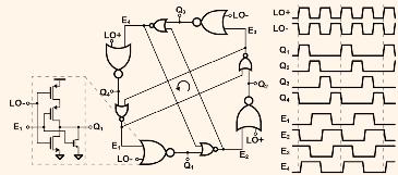
and the 25 percent duty-cycle outputs (Qx, x = 1..4). In this way, we combine a very low-power consumption (41 µW) with low phase noise and mismatch.
What applications could it be used for?
Our design can be used in a wide range of IoT devices, such as wireless earbuds, smartwatches and sensor networks, as well as wireless devices such as keyboards and mice.
Why is it superior to previous designs?
e analog FIR lter makes the receiver over one hundred times more blocker resilient than state-of-the-art designs, which means that the receiver will hold its own in an increasingly crowded wireless environment. On top of that, the total power consumption of the receiver is 370 µW, which is more than two times lower than prior art.
Why is this contribution ISSCC worthy?
anks to several innovations, we achieved unprecedented performance combined with ultra-low power consumption – making our design very relevant for the semiconductor industry. As recognition for this work, Bart ijssen received the Analog Devices Outstanding Student Designer Award – making him the European designer to receive this award.
Imec
First millimeter-scale wireless transceiver for electronic pills
Paper: A 3.5 × 3.8 mm crystal-less MICS transceiver featuring coverages of ±160 ppm carrier frequency o set and 4.8-VSWR antenna impedance for insertable smart pills Presenter, group leader: Minyoung Song, Christian Bachmann Collaborator: University College Dublin
What is your paper about? What did you design?
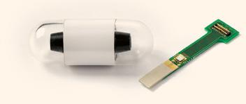
Imec presented the rst fully-integrated mm-scale wireless transceiver for smart insertable pills. e wireless transceiver is implemented in 40nm CMOS and includes an on-chip tunable matching network (TMN) that enables a miniature 400 MHz antenna, and as such avoids external and bulky matching components.
What applications could it be used for?
Autonomous ingestible sensors can measure health parameters such as gut health and transmit in real time the data outside the body. Compared to current procedures like endoscopic inspection and stool sample analysis, this new type of health tracker will make diagnoses of digestive processes and gastrointestinal diseases more comfortable for patients while collecting information over a longer period of time.
Why is it superior to previous designs?
One of the challenges in realizing electronic pills is developing a wireless link that meets the volume, power and performance constraints for reliable data transmission during the period of time that the sensor is collecting data inside the body. Imec’s new wireless transceiver supports the medical 400 MHz frequency bands such as MICS (Medical Implant Communication Service), MEDS (Medical Data Service) or Medradio (Medical Device Radiocommunications Service). e whole transceiver module including antenna occupies a volume of less than 55 mm 3 , which is up to thirty times smaller than state-of-the-art devices. e whole wireless module occupies an area of 3.5 by 15 mm 2 , including a 3.5 by 3.8 mm 2 PCB and a miniature 400 MHz antenna. e small form factor is realized thanks to a new crystal-free transceiver architecture, alleviating the need for an o -chip crystal device, and a 2 mm 2 transceiver IC with the on-chip TMN. Small area is further achieved by a TX/RX shared matching network with only one on-chip inductor and a single-branch phase-tracking RX.
Why is this contribution ISSCC worthy?
It’s a rst breakthrough in realizing autonomous ingestible sensors that can measure health parameters such as gut health and transmit in real time the data outside the body.
Ultra-sensitive and low-power radar
Paper: A 12 mW 10 GHz FMCW PLL based on an integrating DAC with 90 kHz rms frequency error for 23 MHz/µs slope and 1.2 GHz chirp bandwidth Presenter, group leader: Pratap Renukaswamy, Barend van Liempd Collaborator: Vrije Universiteit Brussel
What is your paper about? What did you design?
A novel low-power and extremely accurate phase-locked loop (PLL) for frequencymodulated continuous-wave (FMCW) radars. e radar RF front-end is fully integrated in a 28nm CMOS chip.
What applications could it be used for?
is PLL will be the key building block for a mm-wave motion detection radar at 60 GHz. It can detect movements, recognize gestures and even measure someone’s heartbeat.
Why is it superior to previous designs?
In order to accurately determine the distance and velocity of a target using a FMCW radar, you need a PLL that generates fast and highly linear chirps. You also need to reach a high modulation bandwidth, which determines the resolution of the radar. e big challenge was to design a PLL that meets all these conditions without consuming too much power.
We designed a PLL that achieves the performance targets while consuming only 12 mW power consumption. e PLL generates modulated waves centered around 10 GHz, the frequency of which increases by 1.2 GHz (or 12 percent) in just 51.2 microseconds. e linear increase of 23 MHz per microsecond has an uncertainty (rmsdeviation) of 90 kHz. In its fastest mode, the same bandwidth is covered in only 12.8 microseconds with a rms frequency error of 168 kHz.
Why is this contribution ISSCC worthy?
is low-power PLL is a signi cant step in the development of a low-power 60 GHz radar, of which this PLL is a part. e transceiver details will be published later this year.
Cees Links is a Wi-Fi pioneer and the founder and CEO of Greenpeak Technologies and currently General Manager of Qorvo’s Wireless Connectivity business unit.

Shortening Wi-Fi product design cycles with integrated filtering
One of the most fundamental changes of recent history is that the internet has become nearly ubiquitous. Initially connecting computers, it now connects homes and buildings. And with the advent of wireless technology (Wi-Fi, LTE), access to the internet changed from a technology into a commodity – and, for some people, a number one ranking on Maslow’s hierarchy of needs. Today, any given Wi-Fi network is likely providing simultaneous wireless internet access for multiple laptops, smartphones, tablets and electronic gaming consoles, not to mention the ever-growing installations of smart home or smart business IoT applications.
So, it’s no wonder that interference and coexistence are still the main pain points, more specifically in the area of 2.4 GHz Wi-Fi. The sheer volume of surrounding signals from other wireless products such as Bluetooth speakers, security cameras, smart home devices, remote controls and microwaves is a challenge. The only way to address this interference is by using RF filter technologies.
The companies that make these Wi-Fi-based products depend on quality of service (ie performing well, with few interference issues) to sell their solutions. Products with a high quality of service generate the largest revenue, by reducing the costs of service calls, truck rolls and additional hardware/software solutions needed to solve user experience concerns. Take, for example, a company that manufactures and sells indoor/outdoor wireless speakers. It’s imperative to have a high quality of service to transmit at long range and without interruption. Other adjacent signals like Bluetooth or cellular bands must be attenuated to mitigate interference.
For 2.4 GHz, so-called band edge and coexistence filters are required to solve the issue. For example, discrete band edge filters help to create steep skirts and high attenuation in the out-of-band regions – though with
the tradeoff of providing insertion loss. There are also complete solutions using LTE coexistence filtering and/or band edge filtering, fully integrated in a single front-end package for Wi-Fi 802.11 systems.
A good fully integrated front-end module (FEM) will ideally have a small form factor, high transmit/ receive gains and an integrated high-performance, temperaturestable bulk acoustic wave (BAW) filter. BAW is a technology with superior filtering capabilities. It also provides LTE coexistence receive immunity, maximizing Wi-Fi range and coverage. There are also integrated FEMs that include a transmit and receive 802.11ax module with a band edge BAW filter, regulator, transmit/ receive switch, along with an LNA with bypass opportunity.
Today’s device manufacturers need component products to be plug-andplay and work without extra design effort. This way, they can meet their tight schedules and easily pass regulatory certification. FEMs with integrated BAW filter technology check off these expectations. Additionally, BAW filters resolve interference, and when manufacturers place them in their small, sleek products, they can be assured they’ll meet stringent design criteria when operating at temperature swings of -40 to +105 ºC.
All in all, the opportunities are exciting and vast. Yet, the development of Wi-Fi products is increasing in complexity and the demands on developers to rapidly deliver higher-performance products in aesthetically pleasing designs are growing immensely. No matter the obstacle, developers can achieve their design cycles when they use solutions made to address technology complexities. Just remember, devices such as FEMs with integrated filter technologies are here to help.


