KiCad Fundamentals and Projects
Getting started with the world’s best open-source PCB tool


Peter Dalmaris, PhD


Getting started with the world’s best open-source PCB tool
Peter Dalmaris, PhD
Getting started with the world’s best open-source PCB tool
4th edition covering KiCad 8
●
Peter Dalmaris, PhD
● This is an Elektor Publication. Elektor is the media brand of Elektor International Media B.V.
PO Box 11, NL-6114-ZG Susteren, The Netherlands
Phone: +31 46 4389444
● All rights reserved. No part of this book may be reproduced in any material form, including photocopying, or storing in any medium by electronic means and whether or not transiently or incidentally to some other use of this publication, without the written permission of the copyright holder except in accordance with the provisions of the Copyright Designs and Patents Act 1988 or under the terms of a licence issued by the Copyright Licencing Agency Ltd., 90 Tottenham Court Road, London, England W1P 9HE. Applications for the copyright holder's permission to reproduce any part of the publication should be addressed to the publishers.
● Declaration
The Author and Publisher have used their best efforts in ensuring the correctness of the information contained in this book. They do not assume, and hereby disclaim, any liability to any party for any loss or damage caused by errors or omissions in this book, whether such errors or omissions result from negligence, accident, or any other cause.
All the programs given in the book are Copyright of the Author and Elektor International Media. These programs may only be used for educational purposes. Written permission from the Author or Elektor must be obtained before any of these programs can be used for commercial purposes.
● British Library Cataloguing in Publication Data
A catalogue record for this book is available from the British Library
● This third edition of KiCad Like a Pro consists of two books:
• KiCad Like A Pro | Fundamentals and Projects
Getting started with the world's best open-source PCB tool
590 pages
ISBN: 978-3-89576-626-8 print
ISBN: 978-3-89576-627-5 ebook
• KiCad Like A Pro | Advanced Projects and Recipes
Mastering PCB design with real-world projects
492 pages
ISBN: 978-3-89576-628-2 print
ISBN: 978-3-89576-629-9 ebook
● © Copyright 2024: Elektor International Media B.V.
Prepress Production: D-Vision, Julian van den Berg
Printed in the Netherlands by Ipskamp Printing, Enschede
Elektor is the world's leading source of essential technical information and electronics products for pro engineers, electronics designers, and the companies seeking to engage them. Each day, our international team develops and delivers high-quality content - via a variety of media channels (including magazines, video, digital media, and social media) in several languages - relating to electronics design and DIY electronics. www.elektormagazine.com
4.1.
4.2.
4.9.
5.3.4.
5.3.5.
5.3.6.
8.15.5.
8.15.6.
Please let us know.
Using any web browser, go to txplo.re/kicadr, and fill in the form. We’ll get it fixed right away.
Dr. Peter Dalmaris is an educator, an electrical engineer, an electronics hobbyist, and a Maker. Creator of online video courses on DIY electronics and author of several technical books. Peter has recently released his book ‘Maker Education Revolution’, a book about how Making is changing the way we learn and teach in the 21st century.
As a Chief Tech Explorer since 2013 at Tech Explorations, the company he founded in Sydney, Australia, Peter’s mission is to explore technology and help educate the world.
Tech Explorations offers educational courses and Bootcamps for electronics hobbyists, STEM students, and STEM teachers.
A lifelong learner, Peter’s core skill lies in explaining difficult concepts through video and text. With over 15 years of tertiary teaching experience, Peter has developed a simple yet comprehensive style of teaching that students from all around the world appreciate.
His passion for technology and the world of DIY open-source hardware has been a dominant driver that has guided his personal development and his work through Tech Explorations.
This updated edition of KiCad Like a Pro consists of two complementary but separate books both encompassing KiCad 8. The volume Fundamentals and Projects (590 pages) you are holding now and the volume Advanced Projects and Recipes (492 pages).


KiCad Like a Pro –Fundamentals and Projects:
The book you are holding now!


KiCad Like a Pro –Advanced Projects and Recipes
If you have never used KiCad and have little or no experience in PCB design, please read the introductory Fundamentals and Projects first. It is suitable for readers with little or no experience in PCB design. Then proceed to the Advanced Projects and Recipes.
At the end of both books, you will find recipes, helpful on their own. In the Recipes part, I have dedicated chapters to show you how to complete specific tasks, such as creating a bill of materials or editing text properties. These are basic skills that you will use in most of your projects. Throughout the book, you will find prompts for these recipes to help reduce the need to repeat instructions.
Numerous figures in this book contain screenshots of KiCad. I created these screenshots using KiCad 8.0, which runs on Mac OS. If you are using KiCad under Windows or Linux, do not worry: KiCad works the same across these platforms and even looks almost the same.
Although I cared to produce clear images, this was sometimes impossible. This is particularly true in screenshots of an entire application window meant to be displayed on a large screen. The role of these images is to help you follow the instructions in the book as you are working on your computer. There is no substitute for experimenting and learning by doing, so the best advice I can give is to use this book as a textbook and companion. Whenever you read it, have KiCad open on your computer and follow along with the instructions.
This book has a web page with resources designed to maximize the value it delivers to you, the reader. Please read about the book web page, what it offers, and how to access it on page 14.
Finally, you may be interested in the video course version of this book. This course spans over 25 hours of high-definition video, with detailed explanations and demonstrations of all projects featured in the book. The video lectures capture techniques and procedures that are impossible in text.
will you need
Please check the book web page for updates on this project. Be sure to subscribe to the Tech Explorations email list so I can send you updates.
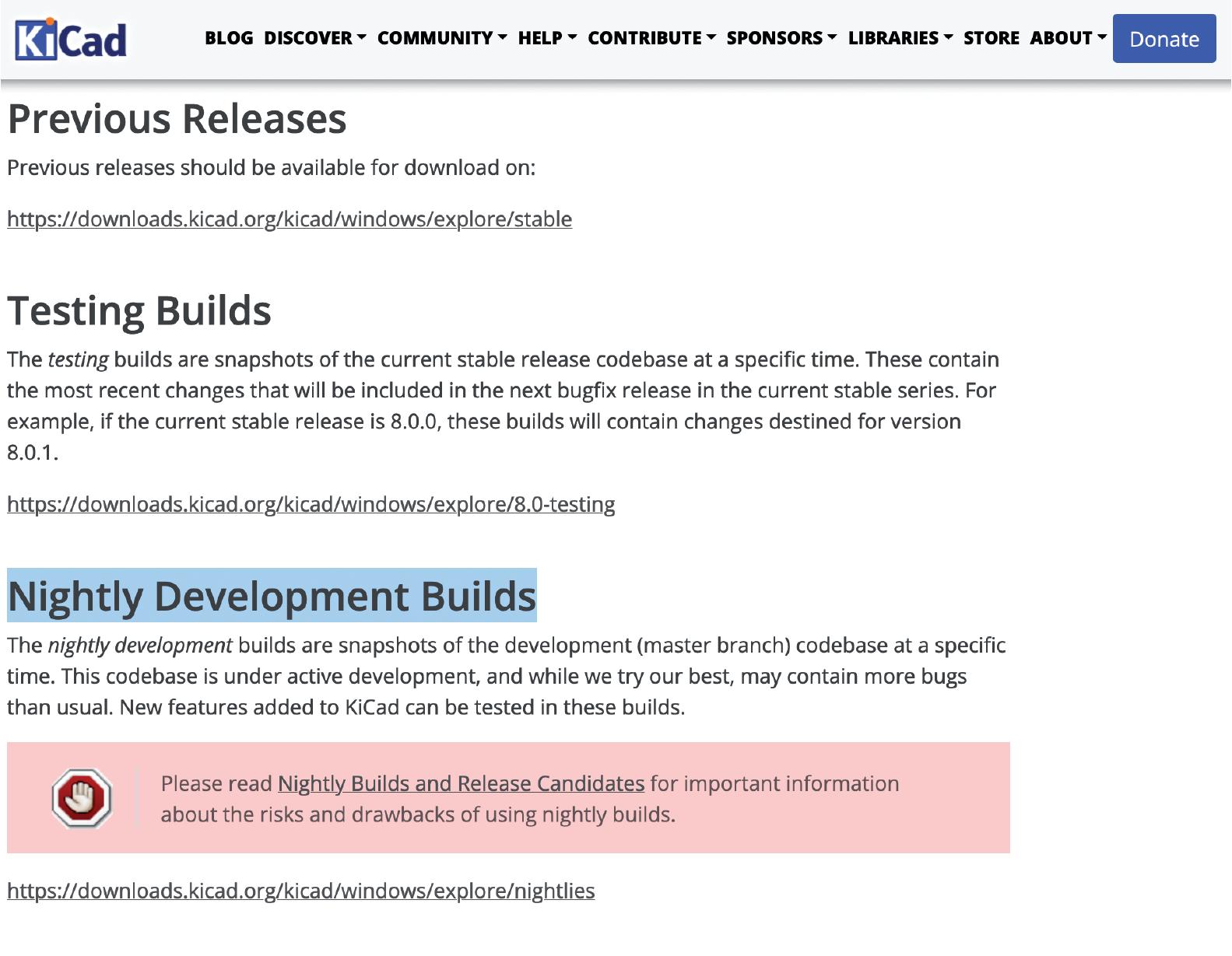
PS1. For an official summary of what’s changed and new in KiCad 8, please read the release announcement on the KiCad blog: https://www.kicad.org/blog/2024/02/Version-8.0.0-Released/
PS2. For a list of all project commits that relate to KiCad 8, please follow this link (it will open the project repository on Gitlab and list all issues with the “8.0” label): https://txplo.re/kicad8_issues
PS3. If you are curious about what will be in KiCad 9, follow this link: https://txplo.re/kicad_8.99_issues
To make the most out of this book, you will need a few things. You probably already have them:
• A computer running Windows, Mac OS or Linux.
• Access to the Internet.
• A mouse with at least two buttons and a scroll wheel. I use a Logitech MX Master 2S mouse (see https://amzn.to/2ClySq0).
- With KiCad 8, it is also possible to use the SpaceMouse device by 3Dconnexion with Windows and Mac OS. I have never used this device. However, some people claim that these mice are more ergonomic and intuitive than regular mice.
• Ability to install software.
• Time to work on the book, and patience.
As a reader of this book, I invite you to access its online resources.
You can access these resources by visiting the book’s web page at https://txplo.re/klp4
The three available resources are:
1. Photos and schematics. Get high-res copies of the book’s photos, schematics, and layouts.
2. Projects. Use the links on this page to download the full KiCad projects from the book.
3. Errata. As I correct bugs, I will post information about these corrections on this page. Please check this page if you suspect that you have found an error. If an error you have found is not listed on the errata page, please use the error report form on the same page to let me know about it.
KiCad 8 was introduced by the KiCad team in early 2024. It represents the next step of evolution for KiCad, with several incremental improvements and additions over KiCad 7.
Jon Evans, one of the lead developers for KiCad, presented the changes in KiCad 8 in a detailed blog post on the KiCad website. You can read this post at this address: https://www.kicad.org/blog/2024/02/Version-8.0.0-Released/
I have updated this book for KiCad 8. In preparation for the update, I first checked all the projects in this book and ensured that they worked in KiCad 8. I am pleased to say that all the projects work properly without modifications.
After ensuring that all projects work properly in KiCad 8, I reviewed the KiCad 8 changes list and documented these changes so that they are presented naturally in the course of this book and its projects.
Because the KiCad 8 changes are “evolutionary” (and not “revolutionary” as they were with KiCad 6), I decided that updating this book is preferable to writing a new one. With KiCad’s new release schedule (essentially, a new major version of KiCad will be published every year), it is not possible for me to write a new book yearly.
To manage the introduction of evolutionary changes into the existing book, I have adopted a system that incorporates changes according to their impact on the PCB design workflow.
For small changes, such as the ability to use custom fonts, I will be inserting “asides”. An aside is a small remark, typically inside a box or as a footnote, that presents the change in line with the rest of the document.
For larger changes, I will introduce new chapters within the existing projects or in the Recipes part.
When a change significantly impacts one of the projects, I will introduce a chapter to that project.
Most changes are documented in new chapters in the Recipes part.
The KiCad 8 user interface is very similar to KiCad 6 and 7. The schematic and layout editors look unchanged without detailed examination. Most dialogue boxes also seem unchanged, except for some widgets (such as text boxes and radio buttons) being moved around. I expect that most people who are familiar with KiCad 6 and 7 will be able to find their way around the KiCad 8 user interface without any trouble.
I used KiCad 8 for all screenshots in this fourth edition of the book.
Wayne Stambaugh
In 1992 Jean-Pierre Charras started the KiCad project. From it’s humble beginnings as one man’s goal to provide an electronics design application for his students to a full fledged open source project with a significant number of contributors, KiCad has become the choice for users who prefer an open source solution for electronics design. As the feature parity gap from proprietary EDAs continues to close, KiCad will continue to become more widely accepted and influential.
One of the enduring hallmarks of a successful open source software project is the publication of a “how to” book. With the publication of “KiCad Like a Pro”, the KiCad project joins the other well known open source projects with that distinction. Whether you are a beginner or a seasoned professional user, this book has something for everyone. From properly configuring and using KiCad to design your first printed circuit board to advanced topics such as using git for version control this book is a valuable resource for any KiCad user.
Thanks to the generosity of author Peter Dalmaris and the publisher Tech Explorations, fifty percent of the profits from the sales of the special fundraising edition of this book will be donated to the KiCad project through CERN. On behalf of all of the developers and contributors of the KiCad project, I thank you for your continued support of the project and your generous contributions.
Wayne Stambaugh KiCad Project Leader
Since KiCad first appeared in the PCB CAD world in 1992, it has gone through 7 major versions and evolved into a serious alternative to commercial products. I have been using KiCad almost daily since version 4, when I published the first edition of KiCad Like a Pro.
Once thought clunky and barely usable, it is now a solid, reliable CAD application. KiCad has been consistently closing the feature and performance gap against its commercial competitors. It has made leaps in adding powerful features and has significantly improved its stability.
Combined with the benefits of free and open-source software, I believe that KiCad is simply the best PCB CAD software for most use cases.
One benefit is KiCad’s active and growing community of users and contributors. KiCad has a dedicated developer team supported by contributing organizations like CERN, the Raspberry Pi Foundation, Arduino LLC, and Digi-Key Electronics. The community is also active in contributing funds to cover development costs. Since joining the Linux Foundation, the KiCad project has received significant development funds in the form of donations from users and industry. The project used this money to buy development time and fund developer conference travel and meetups. To a large extent, this alone guarantees that KiCad’s development will accelerate and continue in the future.
Supporting the KiCad core team is the KiCad community. The community consists of over 250 thousand people worldwide who have downloaded a copy. These people support the KiCad project in various ways: they write code, create and share libraries, and help others learn. They write documentation, record videos, report bugs, and share hacks. During each yearly development cycle, the KiCad repository shows tens of thousands of commits in the source code branches from the developer community. A similarly large number of commits is seem in other parts of the project, such as the libraries and the documentation.
Another signal of the strength of the KiCad community is that KiCad includes completed or nearly completed translations to 12 languages. No other CAD software that I am aware of can boast this.
PCB manufacturers have also taken notice. Many of them now publish KiCad-specific tutorials, explaining how to order your boards. Some have allowed uploading the KiCad native layout file from your project instead of generating multiple Gerber files.
And finally, KiCad is part of an expanding CAD ecosystem. You will find KiCad-compatible component libraries on the Internet’s major repositories, such as Snapeda and Octopart, and native support in PCB project version control software for teams, such as CADLAB.io.
KiCad’s development and prospects have never been brighter than now. KiCad’s post-V8 roadmap has exciting new features and capabilities, such as a new Zone Manager feature, the ability to add comments to ERC and DRC exclusions, and a selection filter for schematic/ symbol editors.
Why do I use KiCad? Because it is the perfect PCB software for my use.
I am an electrical engineer with a background in electronics and computer engineering. But, above all, I am a technology educator and electronics hobbyist. Most of my PCB projects eventually find themselves in my books and courses. My projects are very similar to those of other hobbyists in complexity and size. I make things for my Arduino and Raspberry Pi courses. As a hobbyist, KiCad proved to be the perfect tool for me.
Your use case may be different. You may be a university student completing an engineering degree. You may be a hobbyist or solo developer working in a startup company. You may be part of a team on commercial projects involving highly integrated multi-layer PCBs.
To help you decide whether KiCad is right for you, I have compiled a list of 12 KiCad Benefits. This list contained ten items in the second edition of the book. I added the last two items to highlight additional benefits brought about with KiCad.
Here they are:
Benefit 1: KiCad is open source. This is very important, especially as I spend more time creating new and more complicated boards. Open source, by definition, means that the code base of the application is available for anyone to download and compile on their computer. It is why Linux, Apache, and WordPress essentially run the Internet (all of them open-source). While I am not extreme in my choices between open-source and closedsource software, whenever a no-brainer open-source option does appear, like KiCad, I take it.
Benefit 2: It is free! This is particularly important for hobbyists. CAD tools can be expensive. This worsens with most CAD software companies switching to a subscription-based revenue model. Regular fees do add up when you are a hobbyist or student or bootstrapping for a startup. Not to mention that most of us would not be using even half of the features of commercial CAD software. It is hard to justify spending hundreds of dollars on PCB software when there is KiCad. This brings me to Benefit 3
Benefit 3: KiCad is unlimited. There are no ‘’standard’’, ‘’premium’’ and ‘’platinum’’ versions to choose from. It’s a single download, and you get everything. While there are commercial PCB tools with free licensing for students or hobbyists, there are always restrictions on things like how many layers and how big your board can be, what you can do with it once you have it, who can manufacture it, and much more. There is always the risk that the vendor may change the deal in the future, and you may have to pay a fee to access your projects. I’ll say again: KiCad is unlimited and forever! This is so important that I choose to pay a yearly donation to CERN that is higher than the cost of an Autodesk Eagle license to do my part in helping to maintain this.
Benefit 4: KiCad has awesome features. Professional-grade features include interactive routing, length matching, multi-sheet schematics, configurable rules checker, and differential routing. While you may not need to use some immediately, you will eventually
use them. You can add new features through third-party add-ons. The external autorouter is one example. The ability to automate workflows and extend capabilities through Python scripts is another.
Benefit 5: KiCad is continually improved. Since the publication of KiCad 6, I have seen a very aggressive and successfully implemented roadmap. When I wrote the first version of this book (August 2018), KiCad 5 was about one month old. Three years later, KiCad 6 was delivered with a new architecture and features that set the stage for KiCad’s future development. I am updating this book in March 2024, and KiCad 8 was delivered on schedule a couple of weeks ago, representing an evolution in the history of KiCad, built on the success of KiCad 6. The roadmap ahead looks exciting indeed.
Benefit 6: KiCad’s clear separation of schematics and layout is a bonus to learning and using it. Users of other PCB applications often find this confusing, but I believe that it is an advantage. Schematic design and layout design are indeed two different things. Schematic symbols can be associated with different footprints that depend on the project requirements. You can use the schematic editor independently of the layout editor or in sync. I often create schematic diagrams for my courses that I have no intention of converting into PCBs. I also often create multiple versions of a board using the same schematic. This separation of roles makes both scenarios easy.
Benefit 7: I can make my boards anywhere: I can upload my project to any online fabricator that accepts the industry-standard Gerber files; I can upload it to an increasing number of fabricators that accept the native KiCad layout file; and, of course, I can make them at home using an etching kit.
Benefit 8: KiCad works anywhere. Whether you are a Mac, Windows, or Linux person, you can use KiCad. I use it on all three platforms. I can take my KiCad project from the Mac and continue working on Windows 10 or 11 without worrying about any software or project file glitches. If you use a Mac computer with Apple silicon (such as the M1 and M2 processors), you can now use KiCad 7 natively on your computer instead of relying on the emulation mode.
Benefit 9: KiCad is very configurable. You can assign your favourite keyboard hotkeys and mapping, and with the mouse customisations, you can fully adapt it to your preferences. With the additions of the plugin system and the Python API, extending your instance of KiCad with the exact features you need (or writing them) will be possible.
Benefit 10: If you want to create analog circuits, you will be happy to know that KiCad ships with SPICE. You can draw the schematic in Eeschema and simulate it in SPICE without leaving KiCad. This integration first appeared in KiCad 5, improved over versions 6 and 7, and looks amazing in KiCad 8 with additional simulation types and tighter integration with the schematic editor.
Benefit 11: KiCad’s release cycle was somewhat chaotic in the past. New major versions would come out every two or three years, but no one knew beforehand. In the future, KiCad
will operate in a yearly release cycle. This is good for two reasons: One is commercial users who can now better predict how and when the software they depend on will change. Two, as KiCad users, we can expect a reliable development schedule prioritising reliability. KiCad is now mature enough to evolve predictably.
Benefit 12: KiCad is now a serious productivity tool for businesses. If you are an electronics engineer, you can proudly list it in your resume. If you use it in your business, you can contact the KiCad Services Corporation to customise the software to your requirements. I am talking about deep customisation, not just changing the theme and the menu bars. This means that KiCad can fit precisely with your business. As far as I know, no commercial CAD application can do that. For the non-business users among us, we can expect many of these business-led improvements to flow into future software versions in the tradition of open-source software.
These are the twelve most important reasons I have chosen KiCad as my tool of choice for designing PCBs. These reasons might not suit you, but I hope you will consider reading this book before making your own decision.
I have been using KiCad since version 4. I have packed almost everything I have learned as a KiCad user in this book. I have organised it in a way that will make learning KiCad quick. The objective of this book is to make you productive by the time you complete the first project in part four.
If you come from another PCB CAD tool and have experience designing PCBs, I ask that you have an open mind. KiCad is most certainly very different from your current PCB tool. It looks different, and it behaves differently. It will be easier to learn it if you consciously put aside your expectations and look at KiCad like a beginner would. As per the infamous Borg in Star Trek, ‘’resistance is futile”, in learning, like in so many other aspects of life, you are better off if you go with the flow.
Let’s begin!
1.1. What is a PCB?
As a child, I remember my interest in electronics grew from admiration of what these smart engineers had come up with to curiosity about how these things worked. This curiosity led me to use an old screwdriver to open anything electronic with a screw that fitted.
A record player, VCR, and radio were only a few of my “victims.” I am still surprised that I didn’t get electrocuted. At least I had the good sense to unplug the appliances from the mains. Inside those devices, I found various wondrous things: resistors, transformers, integrated circuits, coils, and power supplies.
Engineers had attached those things on small boards, like the one in Figure 1.1.1. This purple board is an example of a printed circuit board, or PCB, for short.
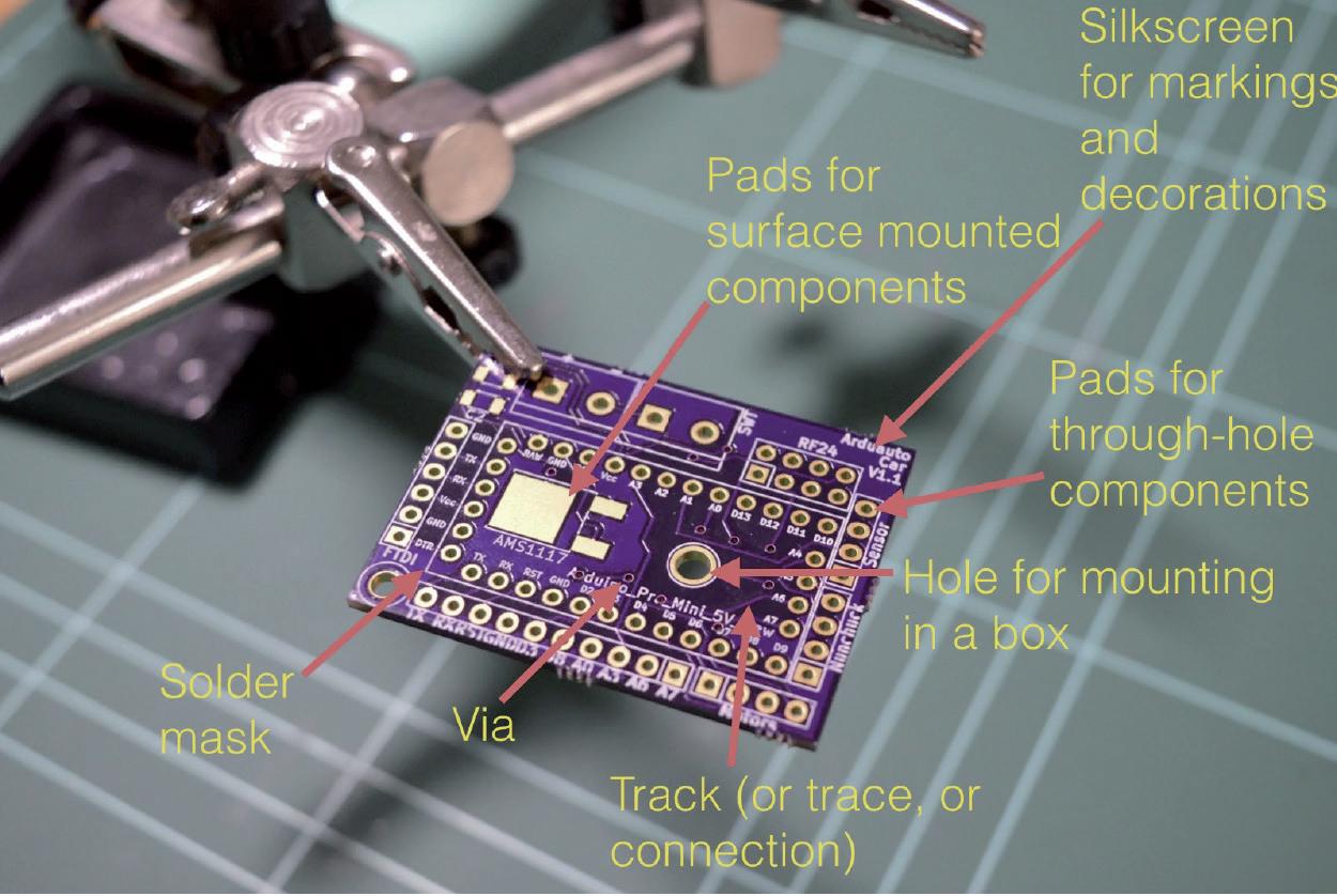
1.1.1: The top side of a printed circuit board.
Let’s look at the components of a PCB, what a PCB looks like, and the terminology we use. The example PCB is one I made for one of my courses (Figure 1.1.1).
The PCB’s top side is where we place the components. Sometimes, we can place components on the bottom side, too.
Generally, there are two kinds of components: through-hole or surface-mounted. We can attach through-hole components on the PCB by inserting the leads or the pins through small holes and using a hot solder to hold them in place. In the example pictured in Figure 1.1.1, you can see several holes to insert the through-hole component pins. The holes extend from the top side to the bottom side of the PCB and are plated with a conductive material. This material is usually tin or gold, as in the case of the board in the image. We use solder to attach and secure a component through its lead onto the pad surrounding the hole (Figure 1.1.2).
If you wish to attach a surface-mounted component, then instead of holes, you attach the component onto the surface of the PCB using tin-plated pads. You will use just enough solder to create a solid connection between the flat connector of the component and the flat pad on the PCB (Figure 1.1.3).

Next is the silkscreen. We use the silkscreen for adding text and graphics. The text can provide helpful information about the board and its components. The graphics can include logos, other decorations, and useful markings.
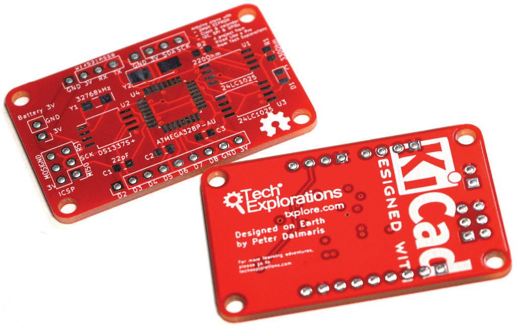
Figure 1.1.4: The white letters and lines is the silkscreen print on this PCB.
In Figure 1.1.4, you can see here that I’ve used white boxes to indicate the location of various components. I’ve used text to indicate the names of the various pins, and I’ve got version numbers up there. It’s a good habit to have a name for the PCB and things of that sort. The silkscreen goes on the top or the bottom of the PCB.
Sometimes, you may want to secure your PCB onto a surface. To do that, you can add a mounting hole. Mounting holes are similar to the other holes in this board, except they don’t need to be tinned. You can use a screw with a nut and bolt on the other side to secure the PCB inside a box.
Next are the tracks. In this example (Figure 1.1.5), they look red because of the color of the masking chemical used by the manufacturer.
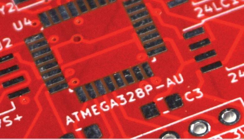
Figure 1.1.5: The bright red lines connecting the holes are tracks.
Tracks are made of copper and electrically connect pins or different parts of the board. You can control the thickness of a track in your design. You can also refer to a “track” as a “trace.”
Notice the small holes that have no pad around them? These are called ‘vias.’ A via looks like a hole but is not used to mount a component. A via allows a track to continue its route in a different layer. If you’re using PCBs with two or more layers, you can use vias to
connect a track from any of the layers to any other. Vias are handy for routing your tracks around the PCB.
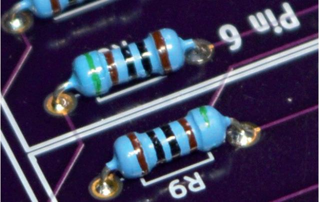
The red substance that you see on the PCB is the solder mask. It does a couple of things. It prevents the copper on the PCB from being oxidised over time. The oxidisation of the copper tracks negatively affects their conductivity. The solder mask prevents oxidisation.
Another thing that the solder mask does is to make it easier to solder by hand. Because pads can be very close to each other, soldering would be complicated without the solder mask. The solder mask prevents hot solder from creating bridges between pads because it prevents it from sticking on the board (Figure 1.1.6). The solder mask prevents bridges because the solder cannot bond with it.
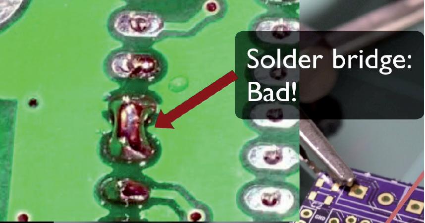
Figure 1.1.6: A solder bridge like this one is a defect that a solder mask can prevent.
Often, the tip of the solder, the soldering iron, is almost as big or sometimes as bigger than the width of the pads. Hence, creating bridges in those circumstances is very easy, and a solder mask helps prevent that from happening.
In Figure 1.1.7 you can see an example of the standard 1.6mm thick PCB.

Figure 1.1.7: This PCB has a thickness of 1.6mm, and is made of fiberglass.
Typically, PCBs are made of fibreglass. The typical thickness of the PCB is 1.6 millimetres. In this close-up view of a PCB picture (Figure 1.1.8), you can see the holes for the throughhole components. The holes for the through-hole components are larger along the edge of the PCB. Notice that they are tined on the inside, electrically connecting the front and back.
1.1.8: A closeup view of the top layer.
In Figure 1.1.8, you can see several vias (the small holes) and tracks, the red solder mask, and the solder mask between the pads. In this close-up, you can also see the detail of the silkscreens. The white ink is what you use in the silkscreen to create the text and graphics.
Figure 1.1.9 is interesting because it shows you a way to connect grounds and VCC pads to large areas of copper, which is called the copper fill.
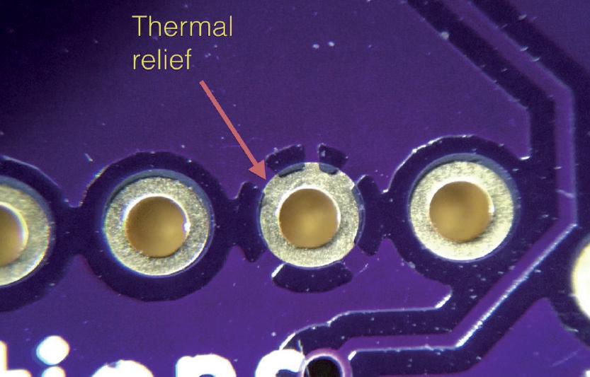
In Figure 1.1.9, the arrow points to a short segment of copper that connects the pad to a large area of copper around it. We refer to this short segment of copper as a ‘thermal relief.’ Thermal reliefs make it easier to solder because the soldering heat won’t dissipate into the large copper area.
Figure 1.1.10 gives a different perspective that allows us to appreciate the thickness of the tracks.
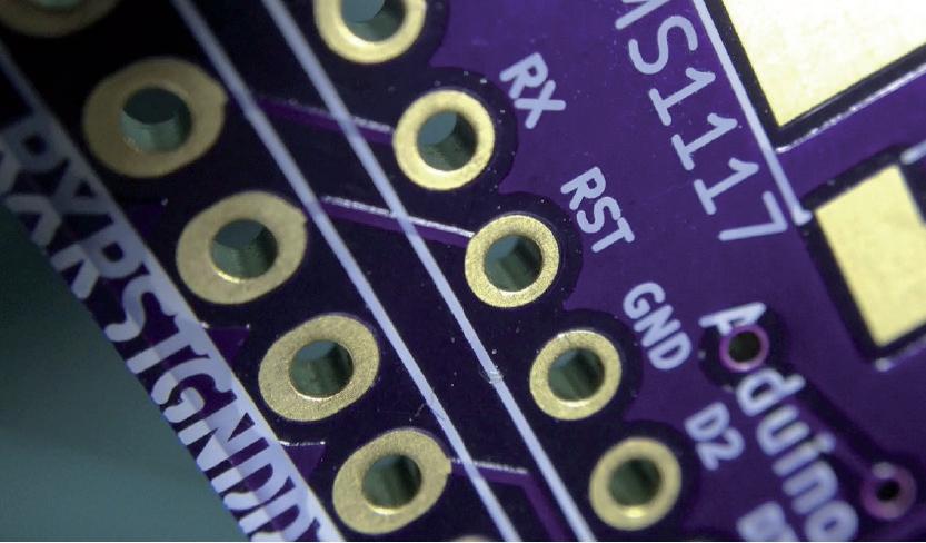
Figure 1.1.10: The holes’ plating covers the hole’s inside and connects that front end with the back end.
Notice the short track that connects the two reset holes (RST)? The light that reflects off the side of the track gives you an idea of the thickness of that copper, which is covered by the purple solder mask.
In this picture, you can also see a very thin layer of gold that covers the hole and the pad and fills the inside of the hole. This is how you electrically have both sides of the hole connected.
Instead of gold plating, you can also use tin plating to reduce manufacturing costs.
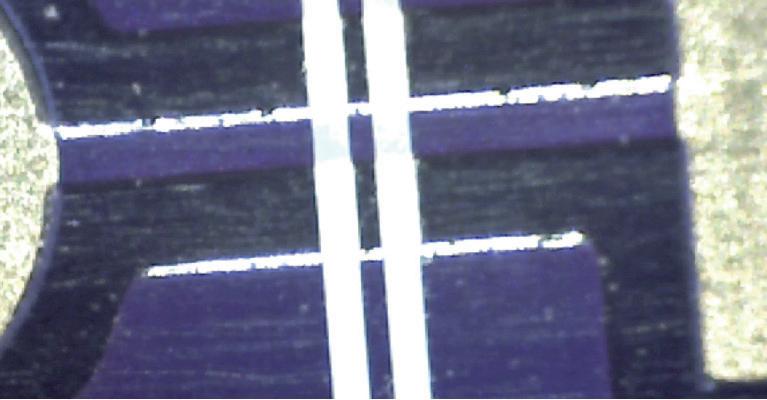
Figure 1.1.11: A detail of this example board at 200 times magnification.
The image in Figure 1.1.11 was taken at 200 times magnification. You can see a track that connects two pads and the light that reflects off one side of the track.
To design a printed circuit board, you must complete several steps, make decisions, and iterate until you are satisfied with the result.
A printed circuit board is a physical device that takes time and money to manufacture. It must be fit to perform its intended purpose and must be manufacturable. Therefore, your design must be high-quality, safe, and possible to manufacture by your chosen manufacturer.
Apart from the practical considerations of designing a PCB, there are also the aesthetic ones. You want your work to look good, not just to function well. Apart from being an engineering discipline, designing a PCB is also a form of art.
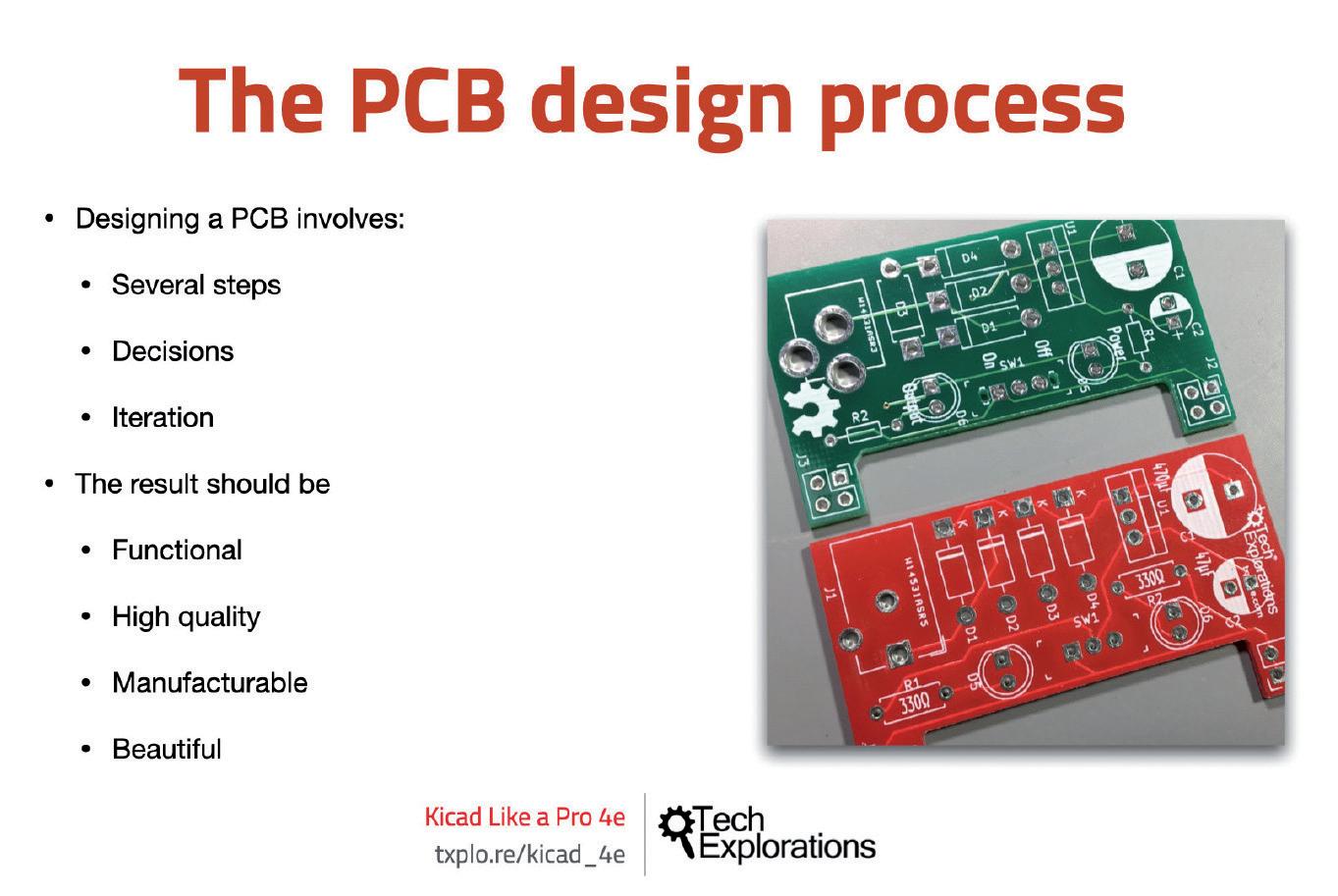
Figure 1.2.1: Some considerations of the PCB design process.
In this book, you will learn about the technical elements of designing a PCB in KiCad, but as you start creating your PCBs, your artistic side will emerge. Over time, your PCB will start to look uniquely yours.
PCB design is concerned with the process of creating the plans for a printed circuit board. It is different from PCB manufacturing. In PCB design, you learn about the tools, process, and guidelines useful for creating such plans.
In PCB manufacturing, on the other hand, you are concerned about the process of converting the plans of a PCB into the actual PCB.
Knowing a few things about PCB manufacturing is useful as a designer of printed circuit boards, though you surely do not need to be an expert. You need to know about the capabilities of a PCB manufacturing facility to ensure that your design does not exceed those capabilities and that your PCBs are manufacturable.
As a designer, you need to understand the design process and the design tools. To want to design a PCB, I assume that you already have a working knowledge of electronics. Designing a PCB, like much else in engineering, is a procedural and iterative process that contains a significant element of personal choice. You will develop your unique design style and process as you build your experience and skills.
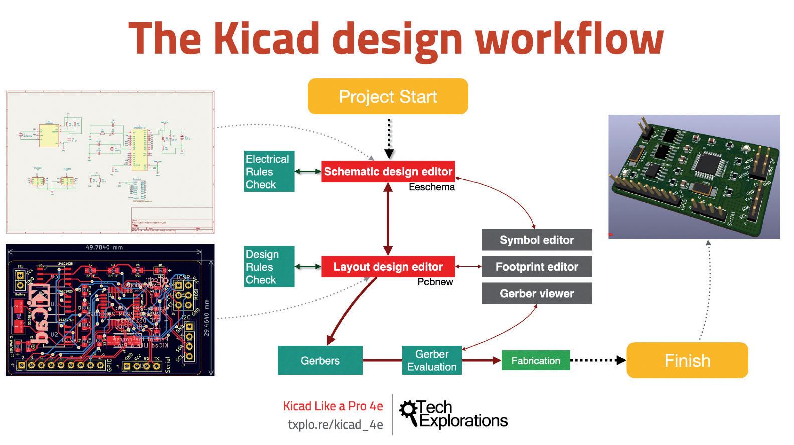
Figure 1.2.2: KiCad is a suite of applications.
KiCad is not a single application. It is a suite of apps that work together to help you create printed circuit boards. As a result, it is possible to customise the PCB design process to suit your particular style and habits. But when you are just starting up, it is helpful to provide a workflow that you can use as a model.
In Figure 1.2.2 you can see my KiCad PCB design workflow model. You can use it as it is or modify it as you see fit. I distilled this workflow by drawing from my experience and learning from other people’s best practices. I also tried to simplify this process and make it suitable for people new to PCB design.
In this book, I will follow this PCB design workflow in all projects.
From a very high-level perspective, the PCB design workflow only has two major steps:
1. Step 1 is the schematic design using the schematic design editor (Eeschema);
2. Step 2 is the layout design using the layout editor (Pcbnew).
Once you have the layout design, you can export and manufacture it.
The schematic design step aims to capture information about the circuit that will be implemented in the final PCB. Once you have a schematic design, you can use the layout editor to create a version of the PCB. Remember, a schematic design can have many different layouts.
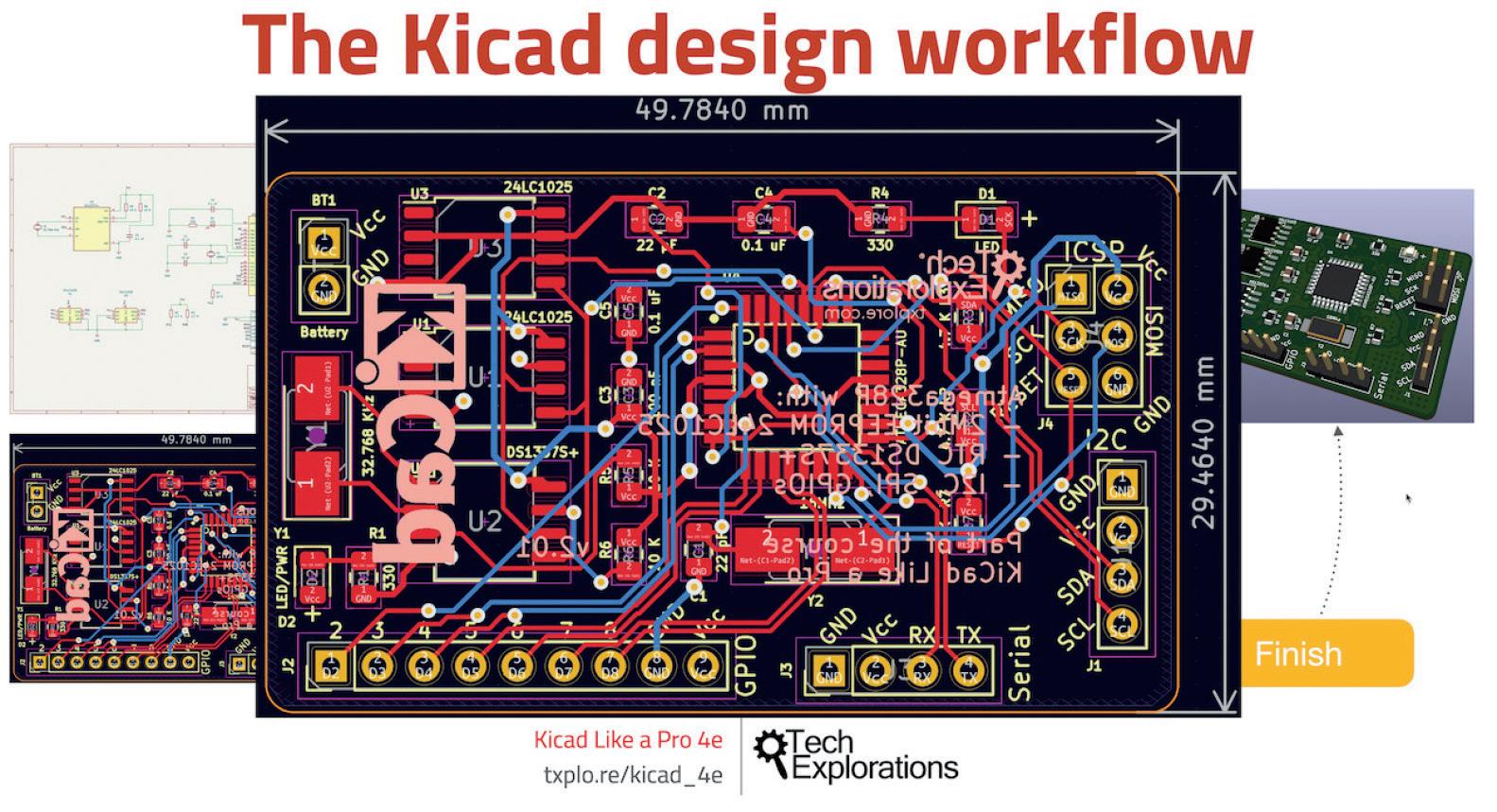
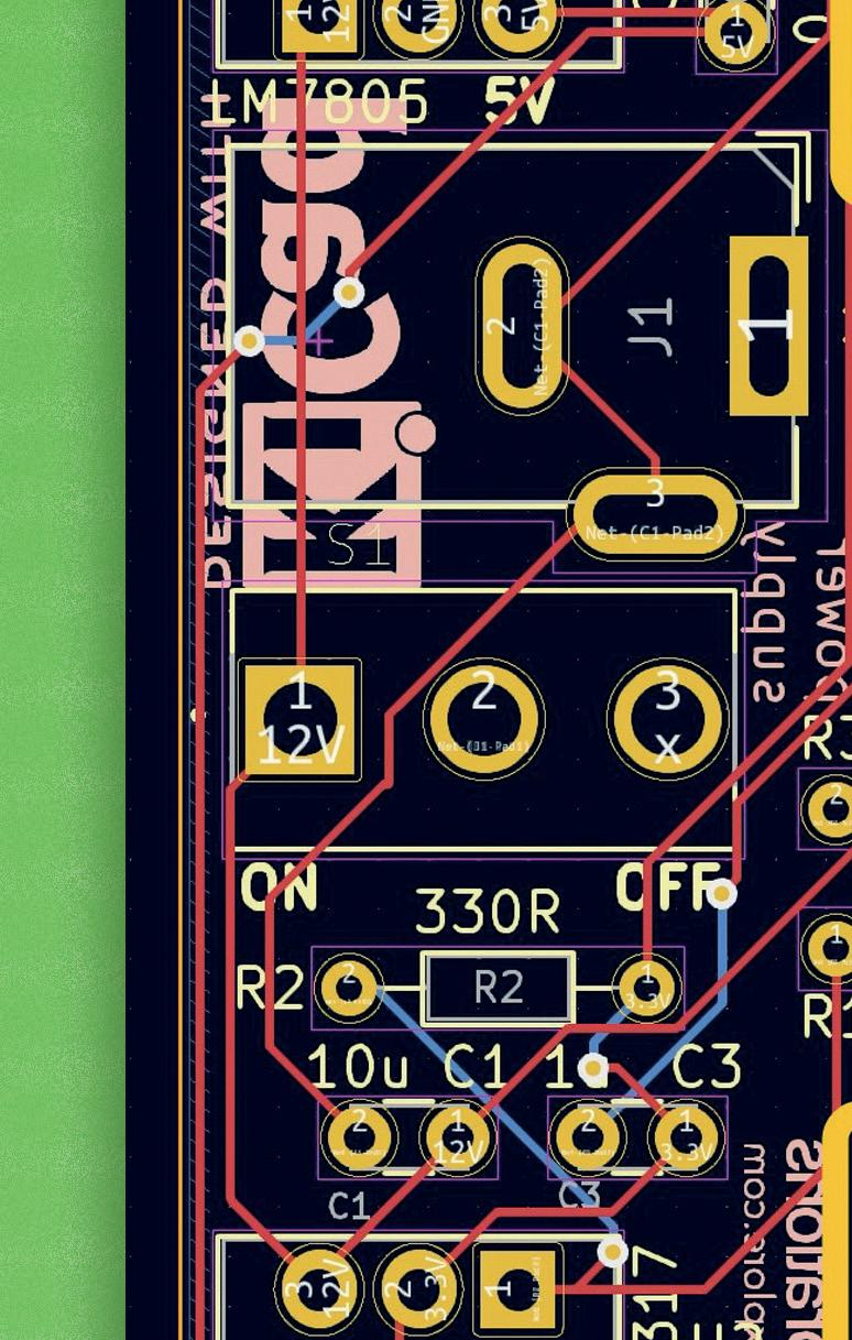
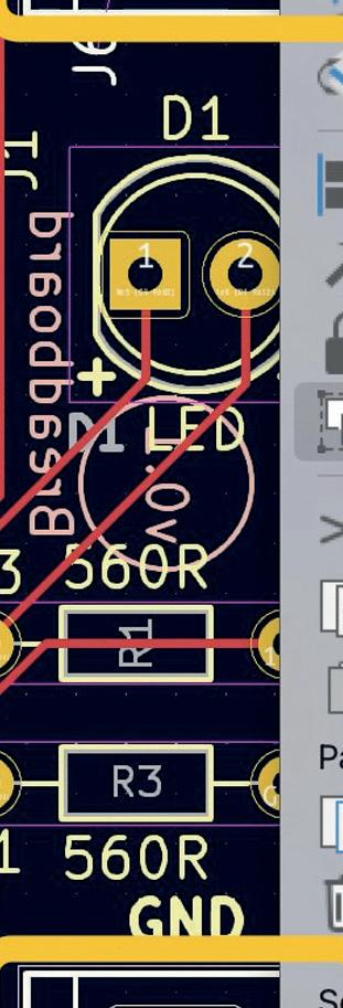
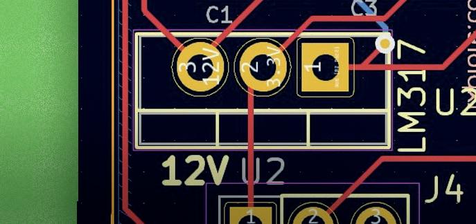
Figure 1.2.3: The KiCad layout file contains information about the physical PCB.
The KiCad layout file contains information about your board, which the manufacturer can use to create the board. The layout must contain information about the size and shape of the board; its construction (such as how many layers it must have); the location of the components on the board; the location of various board elements, like pads, holes, traces and cutouts; the features of these elements (such as the sizes of holes and traces); and much more (which you will learn in detail later in this book).
Let’s walk through the workflow now using the diagram in Figure 1.2.2 as an aid.
For the discussion that follows, keep in mind these definitions:
• A symbol is a symbolic representation of a real component in the schematic; it represents a component’s function, not its physical appearance or location in the final PCB.
• A footprint is a graphical depiction of a real component in the layout. It relates directly to a real physical counterpart. It contains information about the real component’s location and dimensions.
In this book, I will use the terms “symbols” and footprints according to the above definitions.
In KiCad, the process begins with the Layout Editor (or “Eeschema”), the schematic editor.
In the Layout editor, you create the electrical schematic that describes the circuit that will eventually be manufactured into the PCB. You draw the schematic by selecting symbols from the library and adding them to the schematic sheet. If a component you need doesn’t exist in the library, you can search for it on the Internet or create it yourself with the help of the schematic library editor.
Running regular electrical rules checks helps to detect defects early. Eeschema has a builtin checker utility for this purpose.
KiCad’s Layout editor (also “Pcbnew”) has its own validator, the Design Rules Checker.
These two utilities help produce PCBs with a low risk of containing design or electrical defects.
Before you finish work in Eeschema and continue with the layout, you must associate the schematic symbols with layout footprints.
In KiCad, many symbols come with preset symbols to footprint associations, but many don’t, so you’ll have to do this yourself. Also, remember that, as I said earlier, KiCad is very flexible. Assigning many different footprints to the same schematic symbol (one at a time, of course) is possible.
Once you have completed the Electrical Rules Check and symbol to footprint associations, you can continue with a layout using the KiCad Layout design editor or Pcbnew.
You use the Layout editor to position the footprints on the sheet and connect the footprint pins using wires. You’ll also add an outline that marks the outer limit of the PCB and other design elements like mounting holes, logos, and instructional text.
Once you have your PCB laid out and its traces completed, you can do the design rules check. This check looks for defects in the board, such as a trace too close to a pad or two footprints overlapping.
Let’s look at some of the PCB terminology before we continue.
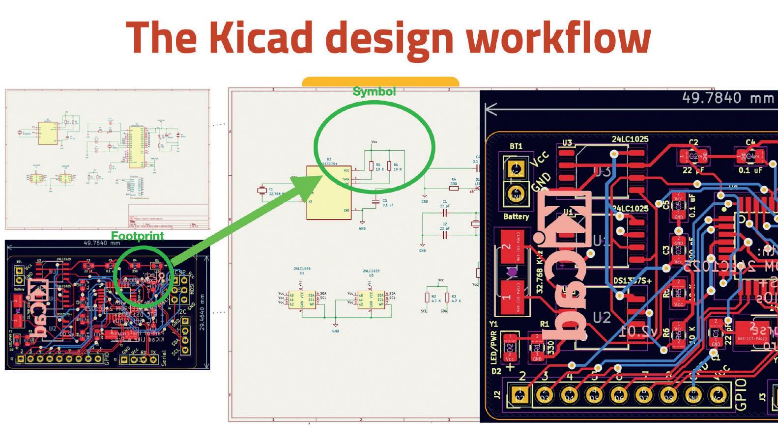
1.2.4: Symbols and footprints.
As you know, a symbol is a symbolic representation of a real component in the schematic. A footprint is a graphical depiction of a real component in the layout.
As the designer, you must tell KiCad which footprint you want to use in your PCB by associating it with a particular symbol. Take the example of a resistor. A resistor uses a specific symbol in the schematic, but it can be realised on the PCB as a through-hole or SMD device of varying sizes.
When you finish working on the layout, you can continue with the last step, which involves exporting the layout information in a format compatible with your board manufacturer’s requirements.
The industry standard for this is a format called ‘Gerber.’ Gerber files contain several related files, with one Gerber file per layer on your PCB, and contain instructions that the fabrication house needs to manufacture your PCB.
Let’s move on to the next chapter, where we’ll talk about fabrication.
1.3. Fabrication
Imagine that you have finished laying out your board in KiCad and are ready to make it. What are your options? One option is to make your PCBs at home. There’s a guide available on the Fritzing website.
The process described in the Fritzing guide is called etching. It involves the use of various chemicals in chemical baths. Some of these chemicals are toxic. You must have special safety equipment and keep your children and pets away. The process emits smelly and potentially dangerous fumes. Once you have your board etched, you still need to use a drill to make holes and vias and figure out how to connect your top and bottom layers.
If this does not sound like your kind of thing (I’m with you!), then you can opt for a professional PCB manufacturer service. NextPCB, and OSH Park are very good at what they offer.
You can get a professionally made PCB for around $15 for several copies without danger to yourself. I’ve extensively used OSHPark (great for beginners, thanks to its straightforward user interface) and NextPCB (great for more advanced projects that need extensive manufacturing options). I’m always happy with the result. Using an online manufacturer takes a little planning because once you order your PCBs, it can take up to several weeks to be delivered. If you’re in a hurry, there are options to expedite the process if you are willing to pay a premium.
The typical small standard two-layer order costs around $10 for a two-square-inch board; you get three copies of that. This price is around $5 per square inch. The pricing is consistent in the industry, where the main cost factor is the size of the PCB. There is a strong incentive to make your PCBs as small as possible. Be aware of this when you design your layout.
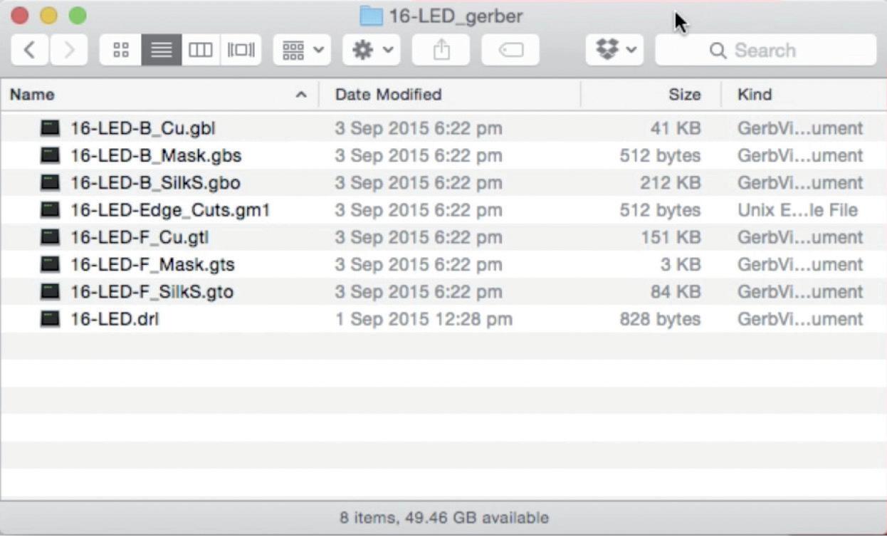
Figure 1.3.1: An example of the Gerber files that the manufacturer will need to make your PCB.
Now, let’s turn our attention to the files you need to upload for these services — and the files are Gerber files. Each layer on your PCB has its own Gerber file, which is simply a text file. The figure below shows the contents of an example Gerber file.
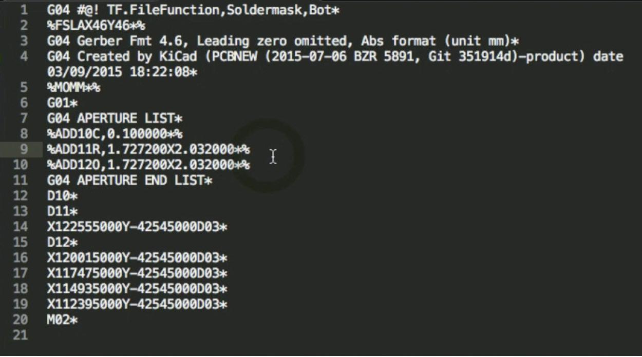
This is just a text-based file containing instructions. An advantage of this text format is that you can use a version control system like Git to maintain your project history and store and share it via online repositories like Github.
Ucamco designed the Gerber file system and standard. They make equipment and write software for PCB manufacturers, including PreCAM software, PCB CAM, laser photoplotters, and direct imaging systems. If you’re curious how to read these Gerber files, you can look up the Gerber format specification on Ucamco’s website.
1.4. Get KiCad for your operating system
It is now time to download your copy of KiCad and install it on your computer.
KiCad supports a variety of operating systems. The major operating systems, Mac OS and Windows are supported. Of course, there is support for Ubuntu and many different flavours
of Linux. I have tested, and I frequently use KiCad on Mac OS. Mac OS is my primary operating system, but I also work on Windows and Kubuntu instead of Ubuntu.
Kubuntu is based on Ubuntu in its core but uses the KDE Desktop and related software. Kubuntu offers a much better experience compared to Ubuntu. Of course, this is my personal preference.
I won’t show you how to install KiCad on each operating system. The KiCad developer team has refined the installer over the years. The KiCad installation process on the supported operating systems is like any other refined application.
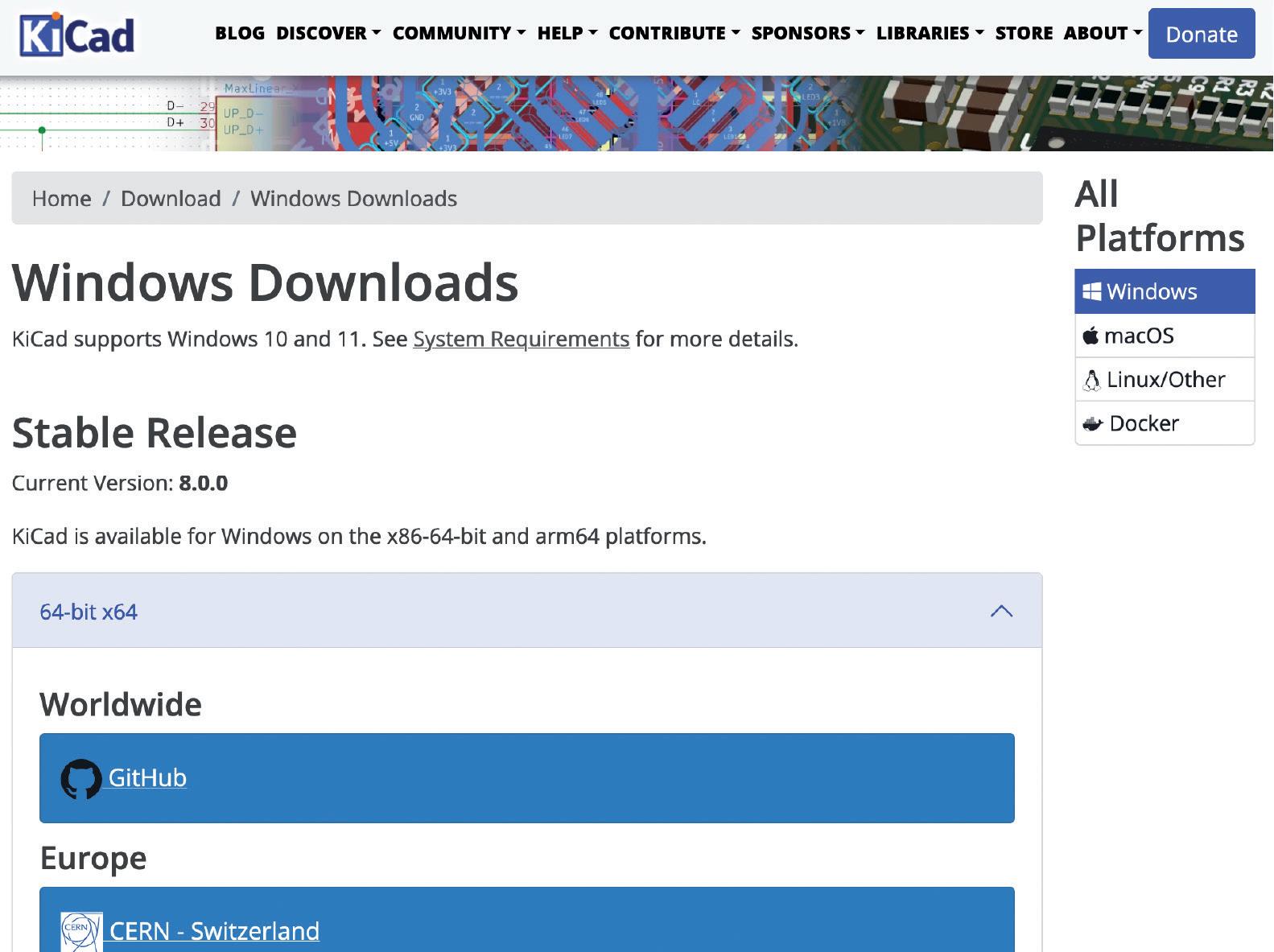
For example, to get the KiCad installer for Windows, go to the KiCad Windows page and download the stable version of KiCad from your preferred source. Double-click on the installer icon and follow the installation wizard instructions to complete the installation on your computer.
1.4.2: Nightly build download
You can download and install the latest version of KiCad available as a nightly build. Nightly builds are work-in-progress. They contain the latest code committed by the KiCad developers but are considered “unstable.” Therefore, you should not use it for work you do not want to lose. The major operating systems have a nightly build generated (almost) every night. If you want to look at the cutting-edge version of KiCad and are not afraid of weird behaviours and strange crashes, then go to the nightly releases page for your preferred operating system and download the installer. Example: Windows.
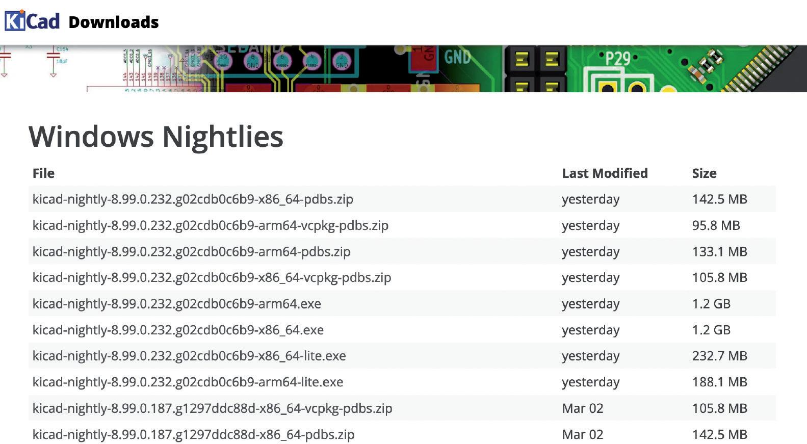
1.4.3: Nightly build download
If you’re working on Mac OS, go to the Mac OS downloads page and download the latest available stable release. You can also download a nightly build if you are comfortable with the inherent risk. Both stable and nightly builds come as a regular DMG file. The download file contains the entire KiCad suite with all its applications, the documentation, and the libraries for the schematic symbols, footprints, and templates. It also includes several demo projects.
The installation process makes use of Ubuntu’s apt-get system. For Ubuntu, you can find installation instructions on the Ubuntu page. You will find instructions for using nightly development builds in Ubuntu on the same page.
Similar instructions exist for various operating systems like Suse and Fedora
You also have the option to download the source code and build from the source on your operating system. This is not something that I usually do unless I want to play around with it and experiment. Luckily, my operating systems have excellent binary builds, so I never needed to build my KiCad instance from the source. But if you enjoy doing that, go to the source code page and follow the detailed instructions.
Now, please download the version of KiCad suitable for your operating system and install KiCad on your computer. Once you finish installing KiCad, verify it’s up and running by starting KiCad.
In the next chapter, you will use your brand new instance of KiCad to look at some demo projects that ship with KiCad.
3D model
3D Models
3D rendering
3D shape
3D shapes
3D viewer 42, 54, 139, 322 , 401, 408 A
99,
101, 185
Footprints 561, 562, 564
Symbols 556, 557, 559, 560
139 Bill of Materials 224, 420, 508, 536
fill
layers
pours
311, , 373, 468
344, 345, 375
468
Board Setup 151, 344, 349
Board Stackup 344, 447
BOM 508, 510, 511, 512, 513, 514, 519, 520, 521, 536, 540 breadboard
custom silkscreen 499
custom symbol 258, 259
D
datasheet 388
Design Analysis Software for
Manufacturability 572
designator 100
Design for Manufacturing 482
Design Rules 151, 354, 448
Design Rules Check 132, 151, 202, 476
Design Rules Checker 30, 304, 324, 352
Design Rules Editor 193
Design Rules group 351
DFM 482, 568, 572, 574, 575, 577, 578, 583
DFM analyser 569
DFM analysis 570
DFM analysis plugin 579
DFM results 570
DFM tests 584
differential track 331
Digikey 247, 361, 424
Digi-Key Electronics 17
Display Grid button 306
Display hidden pins 209
Display options 235
Drawing Sheet editor 59
DRC 132, 151, 202, 352, 476, 477, 488
DRC checks 583
Drill 172
Drill bits 172
Drill Files 412
Drill/place file origin 551
DS1337S 532, 533
E
EasyEDA 515
Edge.Cuts 138 edge cuts layer 126
Editing Options 239, 341
Edit Text & Graphics Properties 489
Edit Track & Via Properties 552
Eeschema 29, 30, 52, 108
Electrical Rules Check 30, 187, 205, 437, 439
Electrical Rules Checker 108, 188, 222, 293
ERC 108, 109, 110, 187, 188, 205, 222, 293, 294, 295, 297, 437 ESP32 417 ESP-WROOM-32 347 etching 31 Excel 511 export 214 External Plugins 517 F
Fabrication Outputs 154, 508 Fast Grid Switching 94 fast-switch grid 98 fault analysis 575 fibreglass 24 Field Name Template 242, 441, 531, 532, 533 filled zone 332, 369, 374 Filter 553, 554 filters 489 flip 218 font 113 footprint 29, 31
Footprint assignment tool 271 footprint editor 55, 220, 321 footprint graphic 507 footprint libraries manager 63
Footprint Library Browser 321
Footprint Manager 541 footprints 195 fp-info-cache 83 fp-lib-table 83 FR-3 166 FR4 165 Freerouting 541 free-standing vias 332 Freetronics 247, 361 Fritzing 31 Fusion360 515 G G-11 166
Generate Drill Files 156 Gerber 31, 32, 154, 410, 415, 476, 568
Gerber File comparator 576
Gerbers 154, 155
Gerber Viewer 56, 57, 157, 413, 415, 569
Gerber Viewer and Analysis 568
GitLab 48, 49
Global Deletions tool 385, 386
Global Design Rules 193
labels 290, 287
Global Libraries 63, 64, 256, 362 Gold fingers
550
overrides 207, 238 , 521, 522, 523
Grids 93, 238
536, 537
and pin highlighter
Netclass assignment list
Netclass assignment patterns
classes 279, 284
Net Classes 280, 353, 354, 437, 438
Net highlighting
label 240 netlabels 278, 284
Net labels 232, 275 nets 106, 187
NextPCB 31, 481, 482, 540, 565, 566, 568, 569, 572, 577, 578, 579, 583
and place
and place machine
Conflicts Map
plated board edge
Plated-through holes
155, 214 plugin 515, 565, 566, 579, 583 Plugin and Content Manager 60, 536, 541, 544, 545
50, 87
361 on/off switch
source
origin 552 origins 334, 343, 547 Origins & Axes 343, 549 OSH Park
124 Outline and constraints
manager 46, 536 Project Specific Libraries 63, 64
514
121, 213
R Raspberry Pi Foundation 17
ratnests 129, 292
ratsnest 309
ratsnest lines 330 rectangle 113 refine 133 reflow oven 178 repeated items 239 Report 570 Report Bug 49 rotate 218, 319 rough outline 122 rounded corners 463
Round Tracks 536
Route tracks tool 130 routing 129, 197
S schematic design 28 schematic design workflow 80, 88, 105 schematic editor 52, 88, 93, 441
Schematic editor preferences 235 schematic hierarchy 217, 286
Schematic hierarchy pane 210
Schematic Setup 213, 294, 437
schematic sheet 285 scope 489, 553, 554
screw terminals 445, 455
Scripting Console 515
search filter 243
Selection Filter 338
Selection & Highlighting 237
Set Track and Via Properties 554
Sheets 511
Shove 377, 378, 497
silkscreen 22, 143, 171, 200, 397, 470, 471
simulator 223 slide switch 175 SMD 167
Snapeda 247, 361, 362 snap to grid 340 solder mask 24, 171 solder paste 176, 177 solid fill 373
Sparkfun 247, 361, 367 SPICE 19
Stencils 177 step 405
surface-mounted 21 swap layers tool 384 symbol 29, 31 symbol and footprint library manager 86
Symbol Choose 243
Symbol Chooser 98, 227
Symbol Editor 49, 55, 218, 260
Symbol Libraries 62
Symbol libraries browser 219 symbol libraries manager 62 symbol library repository 247 Symbol Manager 541 Symbol properties 270 symbol reference designators 298 symbols 164 sym-lib-table 83 System Templates tab 67
T teardrops 524, 523, 525 teardrop shapes 526 terminology 164 text 233
Text & Graphics 448 text label 349, 470 text tool 112, 113
Text Variables 349 TH 167 Theme 546 Themes 544 through-hole 21, 167 THT 420 trace 23 Traces 166 track 331
Track and Via Properties 553
Track outlines 312 tracks 23, 166
Track tool 284
Track width 326
Track Width calculator 58
The latest iteration of KiCad, the world’s best free-to-use Printed Circuit Board tool, is packed with features usually found only in expensive commercial CAD tools. This modern, cross-platform application suite built around schematic and design editors, with auxiliary applications is a stable and mature PCB tool. KiCad 8 is a perfect fit for electronic engineers and makers.
Here are the most significant improvements and features in KiCad 8, both over and under the hood:
> Modern user interface, completely redesigned from earlier versions
> Improved and customizable electrical and design rule checkers
> Theme editor allowing you to customize KiCad on your screen
> Ability to import projects from Eagle, CADSTART, and more
> Python scripting API
> Improved integrated SPICE circuit simulator
> Multi-sheet schematics
> Filters define selectable elements
> Enhanced interactive router helps you draw single tracks and di erential pairs with precision
> New or enhanced tools to draw tracks, measure distances, tune track lengths, etc.
> Advanced interactive router
> Built-in bill of materials generator
> Realistic ray-tracing capable 3D viewer
> Customizable teardrops
> Plug-in manager for quick installation of themes, libraries and functionalities such as autorouters and BOM generators.
This book will teach you to use KiCad through a practical approach. It will help you become productive quickly and start designing your own boards. Example projects illustrate the basic features of KiCad, even if you have no prior knowledge of PCB design. The author describes the entire workflow from schematic entry to the intricacies of finalizing the files for PCB production and o ers sound guidance on the process. Further full-fledged projects, of incremental di iculty, will be presented in a second book, together with a variety of advanced recipes.

Dr. Peter Dalmaris, PhD is an educator, an electrical engineer and Maker. Creator of online video courses on DIY electronics and author of several technical books. As a Chief Tech Explorer since 2013 at Tech Explorations, the company he founded in Sydney, Australia, Peter's mission is to explore technology and help educate the world.


Elektor International Media www.elektor.com