KiCad Advanced Projects and Recipes


Mastering PCB design with real-world projects


Peter Dalmaris, PhD


Mastering PCB design with real-world projects
Peter Dalmaris, PhD
Mastering PCB design with real-world projects
4th edition covering KiCad 8
●
Peter Dalmaris, PhD
● This is an Elektor Publication. Elektor is the media brand of Elektor International Media B.V.
PO Box 11, NL-6114-ZG Susteren, The Netherlands
Phone: +31 46 4389444
● All rights reserved. No part of this book may be reproduced in any material form, including photocopying, or storing in any medium by electronic means and whether or not transiently or incidentally to some other use of this publication, without the written permission of the copyright holder except in accordance with the provisions of the Copyright Designs and Patents Act 1988 or under the terms of a licence issued by the Copyright Licencing Agency Ltd., 90 Tottenham Court Road, London, England W1P 9HE. Applications for the copyright holder's permission to reproduce any part of the publication should be addressed to the publishers.
● Declaration
The Author and Publisher have used their best efforts in ensuring the correctness of the information contained in this book. They do not assume, and hereby disclaim, any liability to any party for any loss or damage caused by errors or omissions in this book, whether such errors or omissions result from negligence, accident, or any other cause.
All the programs given in the book are Copyright of the Author and Elektor International Media. These programs may only be used for educational purposes. Written permission from the Author or Elektor must be obtained before any of these programs can be used for commercial purposes.
● British Library Cataloguing in Publication Data
A catalogue record for this book is available from the British Library
● This third edition of KiCad Like a Pro consists of two books:
• KiCad Like A Pro | Fundamentals and Projects
Getting started with the world's best open-source PCB tool
590 pages
ISBN: 978-3-89576-626-8print
ISBN: 978-3-89576-627-5ebook
• KiCad Like A Pro | Advanced Projects and Recipes
Mastering PCB design with real-world projects
492 pages
ISBN: 978-3-89576-628-2print
ISBN: 978-3-89576-629-9ebook
● © Copyright 2024: Elektor International Media B.V.
Prepress Production: D-Vision, Julian van den Berg
Printed in the Netherlands by Ipskamp Printing, Enschede
Elektor is the world's leading source of essential technical information and electronics products for pro engineers, electronics designers, and the companies seeking to engage them. Each day, our international team develops and delivers high-quality content - via a variety of media channels (including magazines, video, digital media, and social media) in several languages - relating to electronics design and DIY electronics. www.elektormagazine.com
2.2.6.
2.2.7.
2.2.8.
2.3.5.
2.3.6.
3.3.2.
3.8.
3.3.3.
3.3.8.
3.3.9.
4.3.
4.2.1.
4.2.2.
4.2.3.
4.2.7.
4.2.8.
4.2.9.
5.8.
5.9.
5.16.
5.18.
5.23.
5.25.
5.26.
Please let us know. Using any web browser, go to txplo.re/kicadr, and fill in the form. We'll get it fixed right away.
Dr. Peter Dalmaris is an educator, an electrical engineer, an electronics hobbyist, and a Maker. Creator of online video courses on DIY electronics and author of several technical books. Peter has recently released his book 'Maker Education Revolution', a book about how Making is changing the way we learn and teach in the 21st century.
As a Chief Tech Explorer since 2013 at Tech Explorations, the company he founded in Sydney, Australia, Peter's mission is to explore technology and help educate the world.
Tech Explorations offers educational courses and Bootcamps for electronics hobbyists, STEM students, and STEM teachers.
A lifelong learner, Peter's core skill lies in explaining difficult concepts through video and text. With over 15 years of tertiary teaching experience, Peter has developed a simple yet comprehensive style of teaching that students from all around the world appreciate.
His passion for technology and the world of DIY open-source hardware has been a dominant driver that has guided his personal development and his work through Tech Explorations.
This updated edition of KiCad Like a Pro consists of two complementary but separate books encompassing KiCad 8. The volume KiCad Like a Pro – Advanced Projects and Recipes (492 pages) you are holding now includes projects of increasing complexity. It is ideal for readers with a basic working knowledge of KiCad and who have completed the introductory projects described in the book KiCad Like a Pro – Fundamentals and Projects (590 pages).


KiCad Like a Pro –Fundamentals and Projects


KiCad Like a Pro –Advanced Projects and Recipes: The book you are holding now!
If you have never used KiCad and have little or no experience in PCB design, please read the introductory Fundamentals and Projects first. It is suitable for readers with little or no experience in PCB design. Then return to the volume Advanced Projects andRecipes.
At the end of both books, you will find recipes, helpful on their own. In the Recipes part, I have dedicated chapters to show you how to complete specific tasks, such as creating a bill of materials or editing text properties. These are basic skills that you will use in most of your projects. Throughout the book, you will find prompts for these recipes to help reduce the need to repeat instructions.
Numerous figures in this book contain screenshots of KiCad. I created these screenshots using KiCad 8.0, which runs on Mac OS. If you are using KiCad under Windows or Linux, do not worry: KiCad works the same across these platforms and even looks almost the same.
Although I cared to produce clear images, this was sometimes impossible. This is particularly true in screenshots of an entire application window meant to be displayed on a large screen. The role of these images is to help you follow the instructions in the book as you are working on your computer. There is no substitute for experimenting and learning by doing, so the best advice I can give is to use this book as a textbook and companion. Whenever you read it, have KiCad open on your computer and follow along with the instructions.
This book has a web page with resources designed to maximize the value it delivers to you, the reader. Please read about the book web page, what it offers, and how to access it on page 14 in this introductory segment.
Finally, you may be interested in the video course version of this book. This course spans over 25 hours of high-definition video, with detailed explanations and demonstrations of all projects featured in the book. The video lectures capture techniques and procedures that are impossible in text.
Please check the book web page for updates on this project. Be sure to subscribe to the Tech Explorations email list so I can send you updates.
PS1. For an official summary of what’s changed and new in KiCad 8, please read the release announcement on the KiCad blog: https://www.kicad.org/blog/2024/02/Version-8.0.0-Released/
PS2. For a list of all project commits that relate to KiCad 8, please follow this link (it will open the project repository on Gitlab and list all issues with the “8.0” label): https://txplo.re/kicad8_issues
PS3. If you are curious about what will be in KiCad 9, follow this link: https://txplo.re/kicad_8.99_issues
To make the most out of this book, you will need a few things. You probably already have them:
• A computer running Windows, Mac OS or Linux.
• Access to the Internet.
• A mouse with at least two buttons and a scroll wheel. I use a Logitech MX Master 2S mouse (see https://amzn.to/2ClySq0).
- With KiCad 8, it is also possible to use the SpaceMouse device by 3Dconnexion with Windows and Mac OS. I have never used this device. However, some people claim that these mice are more ergonomic and intuitive than regular mice.
• Ability to install software.
• Time to work on the book, and patience.
As a reader of this book, I invite you to access its online resources.
You can access these resources by visiting the book’s web page at https://txplo.re/klp4
The three available resources are:
1. Photos and schematics. Get high-res copies of the book’s photos, schematics, and layouts.
2. Projects. Use the links on this page to download the full KiCad projects from the book.
3. Errata. As I correct bugs, I will post information about these corrections on this page. Please check this page if you suspect that you have found an error. If an error you have found is not listed on the errata page, please use the error report form on the same page to let me know about it.
KiCad 8 was introduced by the KiCad team in early 2024. It represents the next step of evolution for KiCad, with several incremental improvements and additions over KiCad 7.
Jon Evans, one of the lead developers for KiCad, presented the changes in KiCad 8 in a detailed blog post on the KiCad website. You can read this post at this address: https://www.kicad.org/blog/2024/02/Version-8.0.0-Released/
I have updated this book for KiCad 8. In preparation for the update, I first checked all the projects in this book and ensured that they worked in KiCad 8. I am pleased to say that all the projects work properly without modifications.
After ensuring that all projects work properly in KiCad 8, I reviewed the KiCad 8 changes list and documented these changes so that they are presented naturally in the course of this book and its projects.
Because the KiCad 8 changes are "evolutionary" (and not "revolutionary" as they were with KiCad 6), I decided that updating this book is preferable to writing a new one. With KiCad's new release schedule (essentially, a new major version of KiCad will be published every year), it is not possible for me to write a new book yearly.
To manage the introduction of evolutionary changes into the existing book, I have adopted a system that incorporates changes according to their impact on the PCB design workflow.
For small changes, such as the ability to use custom fonts, I will be inserting "asides". An aside is a small remark, typically inside a box or as a footnote, that presents the change in line with the rest of the document.
For larger changes, I will introduce new chapters within the existing projects or in the Recipes part.
When a change significantly impacts one of the projects, I will introduce a chapter to that project.
Most changes are documented in new chapters in the Recipes part.
The KiCad 8 user interface is very similar to KiCad 6 and 7. The schematic and layout editors look unchanged without detailed examination. Most dialogue boxes also seem unchanged, except for some widgets (such as text boxes and radio buttons) being moved around. I expect that most people who are familiar with KiCad 6 and 7 will be able to find their way around the KiCad 8 user interface without any trouble.
I used KiCad 8 for all screenshots in this fourth edition of the book.
by Wayne Stambaugh
In 1992 Jean-Pierre Charras started the KiCad project.From it's humble beginnings as one man's goal to provide an electronics design application for his students to a full fledged open source project with a significant number of contributors, KiCad has become the choice for users who prefer an open source solution for electronics design.As the feature parity gap from proprietary EDAs continues to close, KiCad will continue to become more widely accepted and influential.
One of the enduring hallmarks of a successful open source software project is the publication of a "how to" book.With the publication of "KiCad Like a Pro", the KiCad project joins the other well known open source projects with that distinction.Whether you are a beginner or a seasoned professional user, this book has something for everyone. From properly configuring and using KiCad to design your first printed circuit board to advanced topics such as using git for version control this book is a valuable resource for any KiCad user.
Thanks to the generosity of author Peter Dalmaris and the publisher Tech Explorations, fifty percent of the profits from the sales of the special fundraising edition of this book will be donated to the KiCad project through CERN. On behalf of all of the developers and contributors of the KiCad project, I thank you for your continued support of the project and your generous contributions.
Wayne Stambaugh KiCad Project Leader
Since KiCad first appeared in the PCB CAD world in 1992, it has gone through 7 major versions and evolved into a serious alternative to commercial products. I have been using KiCad almost daily since version 4, when I published the first edition of KiCad Like a Pro.
Once thought clunky and barely usable, it is now a solid, reliable CAD application. KiCad has been consistently closing the feature and performance gap against its commercial competitors. It has made leaps in adding powerful features and has significantly improved its stability.
Combined with the benefits of free and open-source software, I believe that KiCad is simply the best PCB CAD software for most use cases.
One benefit is KiCad's active and growing community of users and contributors. KiCad has a dedicated developer team supported by contributing organizations like CERN, the Raspberry Pi Foundation, Arduino LLC, and Digi-Key Electronics. The community is also active in contributing funds to cover development costs. Since joining the Linux Foundation, the KiCad project has received significant development funds in the form of donations from users and industry. The project used this money to buy development time and fund developer conference travel and meetups. To a large extent, this alone guarantees that KiCad's development will accelerate and continue in the future.
Supporting the KiCad core team is the KiCad community. The community consists of over 250 thousand people worldwide who have downloaded a copy. These people support the KiCad project in various ways: they write code, create and share libraries, and help others learn. They write documentation, record videos, report bugs, and share hacks. During each yearly development cycle, the KiCad repository shows tens of thousands of commits in the source code branches from the developer community. A similarly large number of commits is seem in other parts of the project, such as the libraries and the documentation.
Another signal of the strength of the KiCad community is that KiCad includes completed or nearly completed translations to 12 languages. No other CAD software that I am aware of can boast this.
PCB manufacturers have also taken notice. Many of them now publish KiCad-specific tutorials, explaining how to order your boards. Some have allowed uploading the KiCad native layout file from your project instead of generating multiple Gerber files.
And finally, KiCad is part of an expanding CAD ecosystem. You will find KiCad-compatible component libraries on the Internet's major repositories, such as Snapeda and Octopart, and native support in PCB project version control software for teams, such as CADLAB.io.
KiCad's development and prospects have never been brighter than now. KiCad's post-V8 roadmap has exciting new features and capabilities, such as a new Zone Manager feature, the ability to add comments to ERC and DRC exclusions, and a selection filter for schematic/ symbol editors.
Why do I use KiCad? Because it is the perfect PCB software for my use.
I am an electrical engineer with a background in electronics and computer engineering. But, above all, I am a technology educator and electronics hobbyist. Most of my PCB projects eventually find themselves in my books and courses. My projects are very similar to those of other hobbyists in complexity and size. I make things for my Arduino and Raspberry Pi courses. As a hobbyist, KiCad proved to be the perfect tool for me.
Your use case may be different. You may be a university student completing an engineering degree. You may be a hobbyist or solo developer working in a startup company. You may be part of a team on commercial projects involving highly integrated multi-layer PCBs.
To help you decide whether KiCad is right for you, I have compiled a list of 12 KiCad Benefits. This list contained ten items in the second edition of the book. I added the last two items to highlight additional benefits brought about with KiCad.
Here they are:
Benefit 1: KiCad is open source. This is very important, especially as I spend more time creating new and more complicated boards. Open source, by definition, means that the code base of the application is available for anyone to download and compile on their computer. It is why Linux, Apache, and WordPress essentially run the Internet (all of them open-source). While I am not extreme in my choices between open-source and closedsource software, whenever a no-brainer open-source option does appear, like KiCad, I take it.
Benefit 2: It is free! This is particularly important for hobbyists. CAD tools can be expensive. This worsens with most CAD software companies switching to a subscription-based revenue model. Regular fees do add up when you are a hobbyist or student or bootstrapping for a startup. Not to mention that most of us would not be using even half of the features of commercial CAD software. It is hard to justify spending hundreds of dollars on PCB software when there is KiCad. This brings me to Benefit 3
Benefit 3: KiCad is unlimited. There are no ''standard'', ''premium'' and ''platinum'' versions to choose from. It's a single download, and you get everything. While there are commercial PCB tools with free licensing for students or hobbyists, there are always restrictions on things like how many layers and how big your board can be, what you can do with it once you have it, who can manufacture it, and much more. There is always the risk that the vendor may change the deal in the future, and you may have to pay a fee to access your projects. I'll say again: KiCad is unlimited and forever! This is so important that I choose to pay a yearly donation to CERN that is higher than the cost of an Autodesk Eagle license to do my part in helping to maintain this.
Benefit 4: KiCad has awesome features. Professional-grade features include interactive routing, length matching, multi-sheet schematics, configurable rules checker, and differential routing. While you may not need to use some immediately, you will eventually
use them. You can add new features through third-party add-ons. The external autorouter is one example. The ability to automate workflows and extend capabilities through Python scripts is another.
Benefit 5: KiCad is continually improved. Since the publication of KiCad 6, I have seen a very aggressive and successfully implemented roadmap. When I wrote the first version of this book (August 2018), KiCad 5 was about one month old. Three years later, KiCad 6 was delivered with a new architecture and features that set the stage for KiCad's future development. I am updating this book in March 2024, and KiCad 8 was delivered on schedule a couple of weeks ago, representing an evolution in the history of KiCad, built on the success of KiCad 6. The roadmap ahead looks exciting indeed.
Benefit 6: KiCad's clear separation of schematics and layout is a bonus to learning and using it. Users of other PCB applications often find this confusing, but I believe that it is an advantage. Schematic design and layout design are indeed two different things. Schematic symbols can be associated with different footprints that depend on the project requirements. You can use the schematic editor independently of the layout editor or in sync. I often create schematic diagrams for my courses that I have no intention of converting into PCBs. I also often create multiple versions of a board using the same schematic. This separation of roles makes both scenarios easy.
Benefit 7: I can make my boards anywhere: I can upload my project to any online fabricator that accepts the industry-standard Gerber files; I can upload it to an increasing number of fabricators that accept the native KiCad layout file; and, of course, I can make them at home using an etching kit.
Benefit 8: KiCad works anywhere. Whether you are a Mac, Windows, or Linux person, you can use KiCad. I use it on all three platforms. I can take my KiCad project from the Mac and continue working on Windows 10 or 11 without worrying about any software or project file glitches. If you use a Mac computer with Apple silicon (such as the M1 and M2 processors), you can now use KiCad 7 natively on your computer instead of relying on the emulation mode.
Benefit 9: KiCad is very configurable. You can assign your favourite keyboard hotkeys and mapping, and with the mouse customisations, you can fully adapt it to your preferences. With the additions of the plugin system and the Python API, extending your instance of KiCad with the exact features you need (or writing them) will be possible.
Benefit 10: If you want to create analog circuits, you will be happy to know that KiCad ships with SPICE. You can draw the schematic in Eeschema and simulate it in SPICE without leaving KiCad. This integration first appeared in KiCad 5, improved over versions 6 and 7, and looks amazing in KiCad 8 with additional simulation types and tighter integration with the schematic editor.
Benefit 11: KiCad's release cycle was somewhat chaotic in the past. New major versions would come out every two or three years, but no one knew beforehand. In the future, KiCad
will operate in a yearly release cycle. This is good for two reasons: One is commercial users who can now better predict how and when the software they depend on will change. Two, as KiCad users, we can expect a reliable development schedule prioritising reliability. KiCad is now mature enough to evolve predictably.
Benefit 12: KiCad is now a serious productivity tool for businesses. If you are an electronics engineer, you can proudly list it in your resume. If you use it in your business, you can contact the KiCad Services Corporation to customise the software to your requirements. I am talking about deep customisation, not just changing the theme and the menu bars. This means that KiCad can fit precisely with your business. As far as I know, no commercial CAD application can do that. For the non-business users among us, we can expect many of these business-led improvements to flow into future software versions in the tradition of open-source software.
These are the twelve most important reasons I have chosen KiCad as my tool of choice for designing PCBs. These reasons might not suit you, but I hope you will consider reading this book before making your own decision.
I have been using KiCad since version 4. I have packed almost everything I have learned as a KiCad user in this book. I have organised it in a way that will make learning KiCad quick. The objective of this book is to make you productive by the time you complete the first project in part four.
If you come from another PCB CAD tool and have experience designing PCBs, I ask that you have an open mind. KiCad is most certainly very different from your current PCB tool. It looks different, and it behaves differently. It will be easier to learn it if you consciously put aside your expectations and look at KiCad like a beginner would. As per the infamous Borg in Star Trek, ''resistance is futile", in learning, like in so many other aspects of life, you are better off if you go with the flow.
Let's begin!
Tech Explorations creates educational products for students and hobbyists of electronics who rather utilize their time making awesome gadgets instead of searching endlessly through blog posts and Youtube videos.
We deliver high-quality instructional videos and books through our online learning platform, techexplorations.com.
Supporting our students through their learning journey is our priority, and we do this through our dedicated online community and course forums.
Founded in 2013 by Peter Dalmaris, Tech Explorations was created after Peter realised how difficult it was to find high-quality definitive guides for the Arduino, written or produced by creators who responded to their reader questions.
Peter was frustrated having to search for Youtube videos and blog articles that almost never seemed to be made for the purpose of conveying knowledge.
He decided to create Teach Explorations so that he could produce the educational content that he wished he could find back then.
Tech Explorations courses are designed to be comprehensive, definitive and practical. Whether it is through video, ebook, blog or email, our delivery is personal and conversational.
It is like having a friend showing you something neat... the "AHA" moments just flow!
Peter left his career in Academia after his passion for electronics and making was rekindled with the arrival of his first Arduino. Although he was an electronics hobbyist from a young age, something that led him to study electrical and electronics engineering in University, the Arduino signalled a revolution in the way that electronics is taught and learned.
Peter decided to be a part of this revolution and has never looked back.
We know that even today, with all the information of the world at your fingertips, thanks to Google, and all the components of the world one click away, thanks to eBay, the life of the electronics hobbyist is not easy.
Busy lifestyles leave little time for your hobby, and you want this time to count.
We want to help you to enjoy your hobby. We want you to enjoy learning amazing practical things that you can use to make your own awesome gadgets.
Electronics is a rewarding hobby. Science, engineering, mathematics, art, and curiosity all converge in a tiny circuit with a handful of components.
We want to help you take this journey without delays and frustrations.
Our courses have been used by over 70,000 people across the world.
From prototyping electronics with the Arduino to learning full-stack development with the Raspberry Pi or designing professional-looking printed circuit boards for their awesome gadgets, our students enjoyed taking our courses and improved their making skills dramatically.
Here's what some of them had to say:
"I'm about half way through this course and I am learning so much. Peter is an outstanding instructor. I recommend this course if you really want to learn about the versatility of the amazing Raspberry Pi" -- Scott
"The objectives of this course are uniquely defined and very useful. The instructor explains the material very clearly." -- Huan
"Logical for the beginner. Many things that I did not know so far about Arduino but easy to understand. Also the voice is easy to understand which is unlike many courses about microcontrollers that I have STARTED in the past. Thanks" -- Anthony
Please check outour courses at techexplorations.com and let us be part of your tech adventures.
1.1. Introduction
This chapter focuses on designing a Printed Circuit Board (PCB) based on the Tiny Solar Supply schematic, initially developed by Clemens Valens for Elektor. Valens is an engineer managing the Elektor Labs online platform and has a track record of contributing to projects that serve practical electronic applications. The Tiny Solar Supply is designed to convert solar power into a regulated voltage output, ideal for powering microcontrollers and similar devices.
In the following chapters, I will use KiCad to develop my Tiny Solar Supply based on Clemen's design. I will follow Clemen's original decisions in most of the design, but occasionally I will deviate. I will mainly use symbols and footprints found in KiCad's core libraries but also external libraries when needed.
As with previous projects in this book, I will develop the Tiny Solar Supply project step-bystep. I will start with the schematic's seven steps and continue with the layout.
The original project by Clemens Valens can be found at Elektor Magazine. It provides a foundation for this chapter's exploration of PCB design using KiCad. You can find this project on Elektor's website at https://www.elektormagazine.com/magazine/elektor-305/62009.
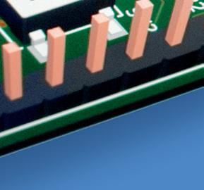
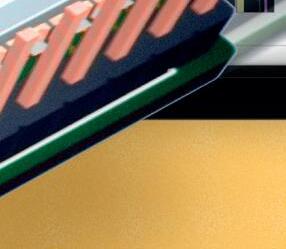
You can see a 3D view of the completed board below.

Here's a summary of what this circuit does and how.
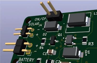
The Tiny Solar Supply is a solar-powered boost converter designed to increase the voltage from a solar panel to a level suitable for powering electronics, such as microcontrollers, that require a stable voltage source. Here's how each part of the circuit contributes to its overall function:
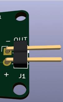
1. Solar Panel and Battery: The solar panel is connected at input K4. During the day, it charges a rechargeable battery (connected at K2). This setup ensures that the device can operate both during the day when sunlight is available and at night using the energy stored in the battery.
2. Boost Converter IC (IC1 - AP3015): The AP3015 step-up DC/DC converter is at the heart of the circuit. This integrated circuit (IC) can work with input voltages as low as 1V and boost them to higher voltages, in this case, a regulated output of 3.3V. The output voltage of the circuit is set by the ratio of resistors R1 to R2, following the formula:

With the specified resistor values, the output is nearly 3.3V.
3. Inductor (L1), Diodes (D1, D2), and Capacitors (C1, C2, C3): These components work together to smooth and stabilize the boosted voltage. The inductor and capacitors form an LC filter that reduces the ripple in the output voltage, ensuring a steady DC supply. Diode D2 prevents the backflow of current from the battery to the solar panel, and diode D1 ensures correct current flow in the boost converter circuit.
4. Transistor (T1 - 2N7002): This transistor acts as a switch controlled by the solar panel's output. During daylight, when the solar panel is active, T1 turns off the boost converter (by pulling the SHDN pin of IC1 low) to save energy. At night, or when the solar panel voltage drops too low, T1 allows the boost converter to turn on, providing a regulated voltage output from the battery.
5. Resistors (R1, R2, R3, R4) and Capacitors (C1, C2, C3): These resistors set the output voltage and ensure the IC's proper operation. Capacitors C1, C2, and C3 help filter the input and output, stabilizing the voltage provided to and from the boost converter.
6. Switch/Control (K3): An optional On/Off switch or jumper can be connected here, offering manual control over the circuit's operation.
This circuit cleverly utilizes solar power to provide a regulated 3.3V output suitable for low-power electronics. Converting and stabilizing the solar panel's variable output ensures a reliable power source for projects operating where traditional power sources are unavailable. Through the assembly and analysis of this circuit in KiCad, students gain hands-on experience with renewable energy applications and voltage conversion and regulation principles.
Here is the schematic of the board:
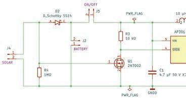
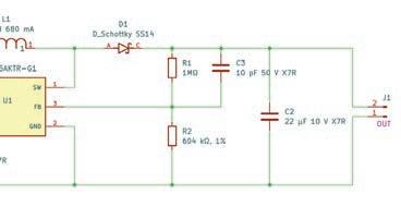
Figure 1.1.2: The project schematic design (final).
Here is the layout:
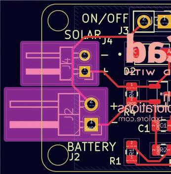
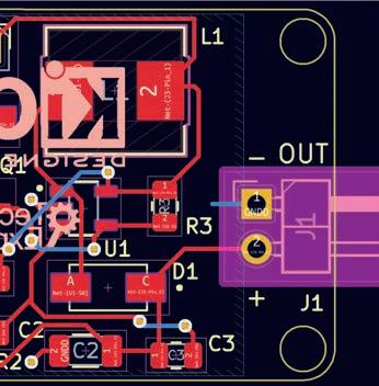
Figure 1.1.3: The project layout design (final).

The actual schematic and design of the board at the end of the process might look slightly different from what you see in the screenshots above.
Below are the components required for this project. I have chosen a footprint different from the one used in the original Elektor project for some components.
ReferenceValue
Footprint
R1, R41 MΩ, 0.125 W 0805, Resistor_SMD:R_0805_2012Metric
R2 604 kΩ, 1%, 0.125 W0805, Resistor_SMD:R_0805_2012Metric
R3 10 kΩ, 0.125 W 0805, Resistor_SMD:R_0805_2012Metric
C1 4.7 µF, 50 V, X7R0805, Capacitor_SMD:C_0805_2012Metric
C2 22 µF, 10 V, X7R1206, Capacitor_SMD:C_1206_3216Metric
C3 10 pF, 50 V, X7R0805, Capacitor_SMD:C_0805_2012Metric
L1 10 µH, 680 mA
IND_ASPI-0630LR_ABR (external library from Ultralibrarian)
D1, D2SS14
IC1 AP3015A
DO-214AC, DIOM4325X250N (external library from Snapeda)
AP3015AKTR-G1:SOT95P280X145-5N (external library from Snapeda)
T1 2N7002 SOT-23
J1, J2, J3
J4
pin header, 1 row, 2 contacts
2.54 mm pitch, right-angle
pin header, 1 row, 2 contacts 2 mm pitch
We'll design this PCB with two copper layers and a GND copper fill in the bottom layer.
Let's begin with the schematic design process.
In this chapter, you will complete the schematic design of this PCB by following the schematic design workflow (see below). You learned about this workflow in Part 6 of the book.
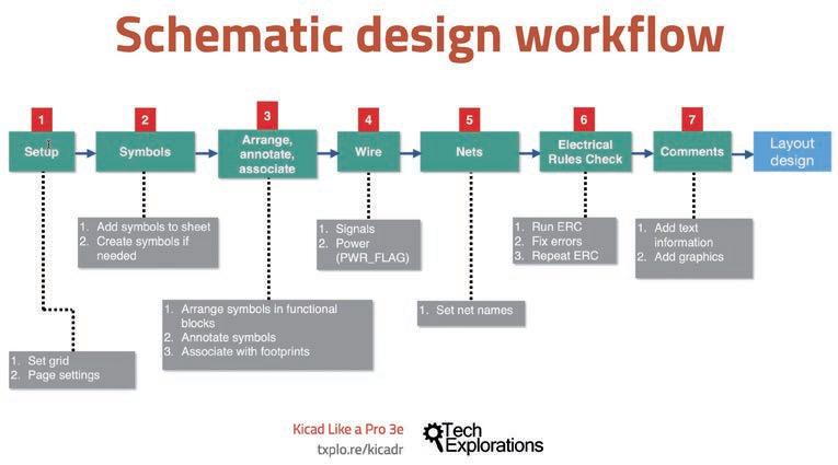
Figure 1.2.1: The schematic design workflow.
Unlike the simple project you completed in Part 3 of the book, you will use the model workflow more realistically in this project. Instead of using it linearly, there will be cases where you must return to a previous step, fix or improve something, and then continue.
Time to start.
Open KiCad and create a new project. Give the project a name. I have called mine "Tiny Solar Supply" and saved it in my projects folder.
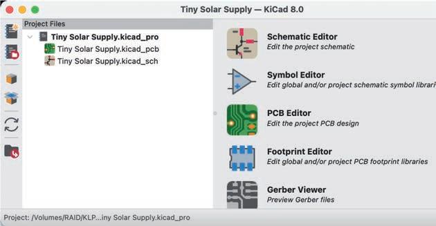
Figure 1.2.1.1: The new KiCad project.
In the project folder, you will see three files:
• The project file: "Tiny Solar Supply.kicad_pro".
• The layout file: "Tiny Solar Supply.kicad_pcb".
• The schematic file: "Tiny Solar Supply.kicad_sch".

Click on the Schematic Editor in the project window to start the schematic editor. The schematic sheet is empty. Let's do a basic setup for the project.
Bring up the Schematic Setup window (File—> Schematic Setup, or click the Setup button from the top toolbar). Review the schematic settings. I will leave these settings as their defaults and add Net Classes later in the project.
Similarly, in the KiCad Preferences window, I will use the default settings. In the Display Options tab (under Preferences—> Schematic Editor), I have set "Snap to Grid" to "Always"and "Cursor Shape" to "Full window crosshair."
In the Editing Options tab, I have selected the Line drawing mode option to "90 deg Angle".
In the Colors tab, I have changed the background color of my theme to white so that the screenshots on these pages look better (the default background color is light grey).
The last setup item in my list is to enter the project details in the Page Settings window. Bring up this window (File —> Page Settings or click the Settings button from the top toolbar). Fill in the text fields with the information you want to show in the sheet's information corner. Also, select a sheet size and enter the issue date. You can see my Page Settings window below:
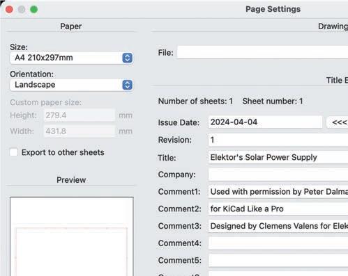

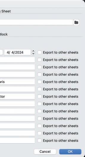
Figure 1.2.1.2: The schematic editor page settings.
This information will appear in the bottom-right corner of the schematic sheet.
The setup is complete; let's continue with step two, adding the component symbols on the editor sheet.
1.2.2. 2 - Symbols
Let's find the required symbols and drop them on the design sheet. Most symbols are available in the KiCad libraries, but you'll have to import one from Snapeda and another from Ultralibrarian. Use the table in the introduction to help you locate the symbols.
Start with the symbols from the KiCad libraries. These are the resistors, capacitors, connectors, and transistors. Here's my sheet at this point:
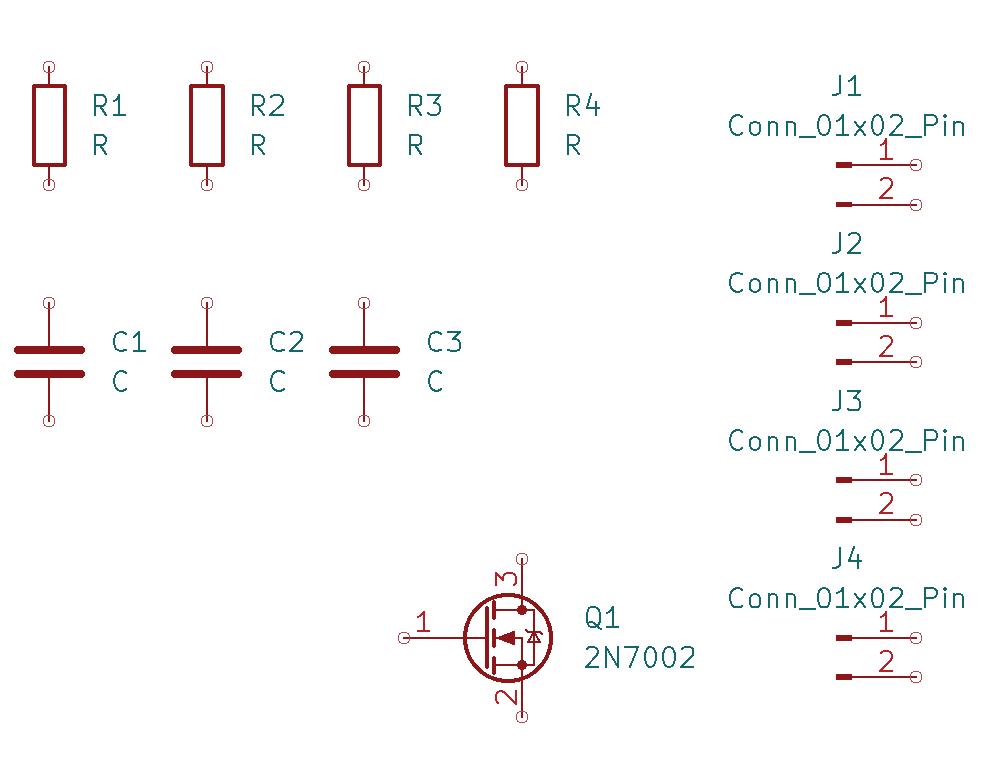
Figure 1.2.2.1: The symbols are from the KiCad libraries.
I could not find suitable symbols for the inductor (L1), the Schottky rectifiers (D1 and D2), and the IC (U1), so I looked online. I found the IC (AP3015AKTR-G1) and inductor on Ultralibrarian and D1-2 on Snapeda:
• U1 (AP3015AKTR Micro Power Step-Up DC-DC Converter): https://txplo.re/AP3015AKTR
• D1, D2 (Schottky rectifier) ASPI-0630LR-100M-T15 inductor): https://txplo.re/ss14
• L1 (inductor): https://txplo.re/coil
Download and install these parts' symbols, footprints, and 3D models. The easiest way is to download the ZIP files for the two parts and copy them into the project folder. Below, you can see my project folder after copying the external libraries.
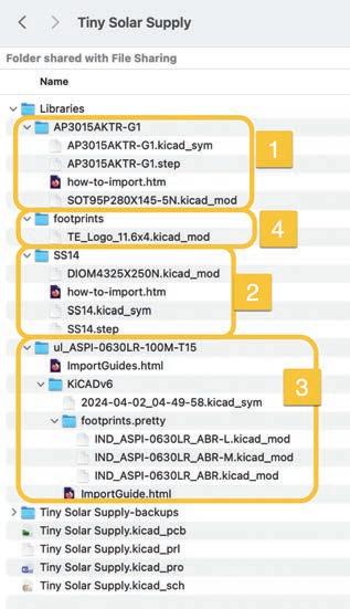
Figure 1.2.2.2: The imported libraries in my project folder.
Regarding the number in the screenshot above, "1" is the U1 integrated circuit symbol and footprint, "2" is the SS14 Schottky diode, and 3 is the L1 coil. I have also added a footprint for the Tech Explorations logo, a non-functional footprint that I will use to decorate the back of the board.
After copying the libraries to the project folder, install them on KiCad. I did this for the project only. You can see my Symbol and Footprint properties windows below:
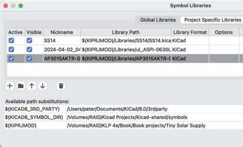
Figure 1.2.2.3: The external symbols installed for the project.
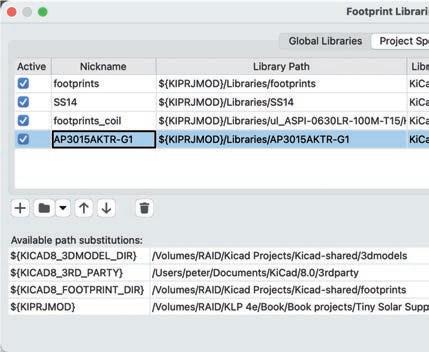
Figure 1.2.2.4: The external footprints installed for the project.
Now that the last required symbols are available for the project, add them to the schematic sheet. Here's my schematic sheet:
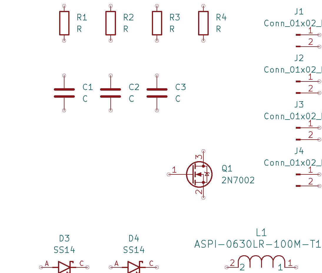
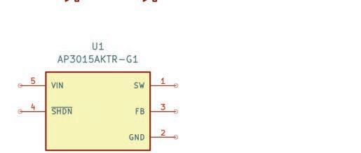
Figure 1.2.2.5: All project symbols are ready to arrange and connect.
Before you continue step three of the workflow, arranging, annotating, and associating the symbols, you will add component values to the capacitors and resistors.
Let's continue by editing the value for the capacitors and resistors. The value for each component is included in the introduction of the components table. Unlike how I did this previously (i.e. by opening the properties of each symbol separately), this time, I will edit the component values in bulk using the Symbol Fields Table window. This will allow me to edit all values in one operation. You can open this window by clicking the table button in the top toolbar.
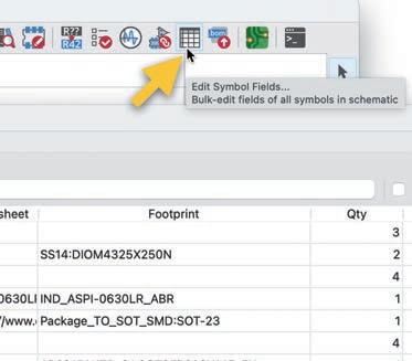
Figure 1.2.3.1: Open the Edit Symbol Fields window.
In this table, components are grouped by type. Click on the ">" symbol to expand each category so that you can edit their value individually. Notice that even though this table also allows you to edit the footprints, I will leave this for later and concentrate on the values for the time being.
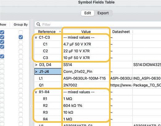

Figure 1.2.3.2: Edited values for the capacitors and resistors in the Symbol Fields Table.
Click OK to submit the changes to the table and close the window. The schematic sheet now should look like this:
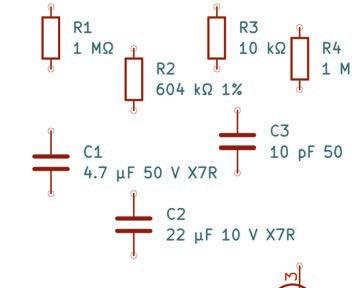
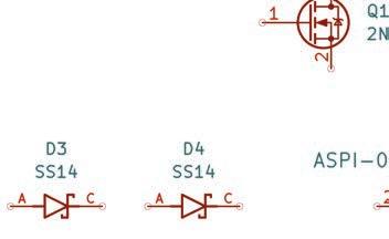
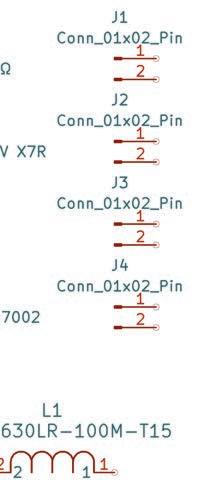
Figure 1.2.3.3: The schematic sheet, with values assigned to the capacitors and resistors.
Step two is complete. Let's continue with Step three, where you will arrange the symbols according to their functional group and associate them with footprints.
1.2.4. 3 - Arrange, Annotate, Associate
Step three of the schematic design workflow is where we:
1. Rearrange the symbols to the (usually) final locations in the sheet.
2. Annotate the symbols with their unique identifiers.
3. ssociate the symbols with the footprints we'd like to use in the layout.
Since KiCad 7, annotation happens automatically when you drop a symbol on the schematic editor sheet (unless you have disabled the auto-annotation feature). Nevertheless, I will take the opportunity to ensure that all symbols are correctly annotated and valued.
Let's begin.
Arrange
This is the easiest part of the entire project. Clemens designed the circuit (in KiCad 6!) and published it on Elektor. So, I stepped on his shoulders and copied his design, starting with the location of the symbols.
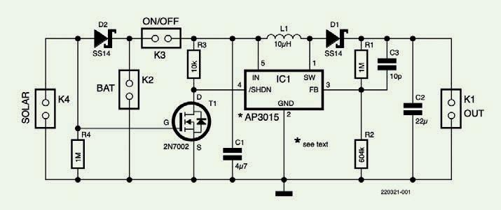
Figure 1.2.4.1: Clemen's design. I will copy it!
I'll move and orient the symbols so they are ready to wire in the next step. I'm using Clemens's original circuit as a guide. Here is my schematic with the symbols arranged:
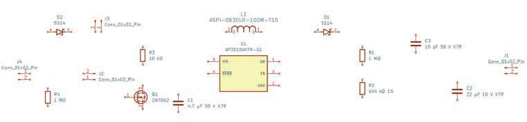
Figure 1.2.4.2: My schematic, with the symbols arranged.
In KiCad 8, as with KiCad 7, symbols are automatically given a unique identifier when you add them to the schematic sheet. As a result, I don't have any symbols that require annotation. However, I will take this opportunity to inspect all symbols and ensure that their reference designators match those shown in the parts table in the introduction of this project.
Once I'm satisfied that they do, I will continue with the association task.
In this task, I will associate symbols with footprints. I will associate the resistors, capacitors, pin headers, and transistors with footprints available in KiCad's footprints library and the coil, diodes, and DC/DC converter with footprints in the external libraries. You should have installed these external footprints and their symbols at the start of this project. Use the table in the introduction for guidance on the footprints for each symbol.
The only through-hole components on this board are the pin headers. Below, you can see my associations table:
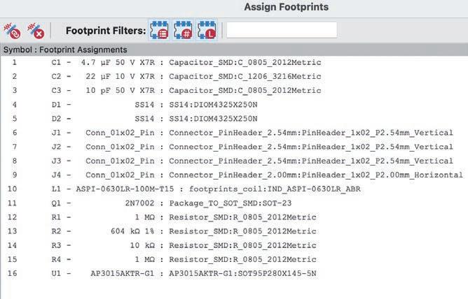
Figure 1.2.4.3: The symbol and footprint associations.
This completes step three of the workflow. Let's continue with the wiring in the next segment.
2D Barcode
3D model
3D models 63, 148, 222
3D shapes 144, 151
3D STEP files
3D viewer 116, 150, 217, 222
4x8x8 LED Matrix Clock
8x8 LED display
8x8 LED matrix display 73, 74 0402 257, 285
486
Appearance 126, 215, 246
Arduino 75, 77, 83, 84
Arduino Pro Mini 773, 5, 77, 82, 114, 117, 139
Arduino Pro Mini footprint
Atmega328P 73, 240, 352, 354
Atmega328P-AU 158, 185
copper fills 51, 201, 307, 308, 310 copper fill zones
CP2102N 259, 322 custom and advanced functionality482
Custom Rule 348
Custom Rules 344, 345, 347
custom schematic sheet 464
Customs Rules 345 custom user templates 456
D data logger 158
DC/DC converter 24 defects 341
Design for Manufacturing 70
Design Rules 102
Design Rules and net classes 337
Design Rules Check61, 136, 216, 315, 348
Design Rules Checker341, 342, 377
design rule violations 344
DFM 70
DFM checklist 70
DFM report 321
diff 414
differential pair 305, 381, 388
differential pair routes 305
differential pair tracks 384
Differential skew 389
Digikey 81
DIP 392
DRC 54, 75, 123, 128, 136, 142, 144, 200, 215, 216, 228, 230, 248, 298, 301, 310, 327, 342, 347, 348
drill files 317
Drill Holes 375
E Eagle 364, 432
EasyEDA 432
Edge.Cuts104, 106, 115, 116, 117, 286
Edge.Cuts layer 116
Edit Text and Graphic Properties301
EEPROM 193, 224
EEPROMs 158
Electrical Rules Check38, 94, 183, 275
Electrical Rules Checker 348
Elektor 23, 34
Elektor Labs 23
Elektor Magazine 23
ERC 91, 94, 96, 184, 186, 275, 348, 350
ERC errors 207 Error 350
ESP32 252, 272, 281, 285, 290, 298, 304, 322
ESP32 development kit 253, 256
ESP32 dev kit 252
ESP32-DevKitC-v4 256 "ESP32-DevKitC-V4 269
ESP32-SOLO-1 269
ESP32WROOM-32 260 Espressif 252, 270
F
"Fill All Zones" 204 Find and Replace 330, 331 Footprint Editor 391, 392 footprint generator 393 footprint placement 107 footprints 342 Footprint Wizard 391 Fortran 436 four-layer 227 Freerouting 362, 363, 367, 369 f-string formatting 478
Gerber 63, 67, 104, 142, 217, 222, 316, 327
Gerbers 165, 225
Gerber Viewer67, 142, 143, 218, 231, 319
Gerber ZIP 219
GetBoard 476, 477, 480
GetFootprints 477 git 422
Git 158, 162, 167, 188, 189, 222, 225, 230, 398, 403, 404, 413 gitattributes 234, 235 git branch 233, 414, 419, 422 git checkout 416
Git commit 234 git diff 413 GitHub 403, 419 gitignore 408, 409 git log 416
171, 173, 175, 179, 189, 201, 206, 227
NextPCB 67, 144, 199, 218, 219, 283, 299, 317 NextPCB Active Manufacturing
nextpcb.com
NextPCB online Gerber viewer 319
NextPCB's DFM tool 72
NextPCB's KiCad plugin 319
NextPCB's online Gerber viewer232
PCB
PCB
91, 186
Python 472, 486
API 472, 478, 480, 486
129, 134, 139, 143, 210, 217, 301, 312, 313, 337
code
28, 63, 77, 81, 162, 167, 259, 322, 354, 355, 357
436, 438, 439, 444
T
355 text label 301
Text properties 335
text variable 80, 334, 335, 336
Text Variables 332 theme 429
Tiny Solar Supply 23, 27 TQFP 223
Track length tuning 385 tracks 122
Tracks and Vias overrides 48 Track Width calculator
Transistors
U
UART
74, 259
Ultralibrarian 28, 63
un-archive 458
Unconnected 278
USB 74, 259, 285
USB connector 322
V
version control 398 violations 62, 230, 315
Violation Severity43, 342, 341, 344, 348
violation severity classifier 341
Violation Severity settings341, 342
W
Walk around 197, 304 warnings 55, 140, 350
Warning: Text thickness out of range139 wire tool 37 wiring 36 X
This book builts on KiCad Like a Pro Fundamentals and Projects and aims to help you practice your new KiCad skills by challenging you in a series of real-world projects. The projects are supported by a comprehensive set of recipes with detailed instructions on how to achieve a variety of simple and complex tasks. Design the PCBs for a solar power supply, an LED matrix array, an Arduino-powered datalogger, and a custom ESP32 board. Understand the finer details of the interactive router, how to manage KiCad project teams with Git, how to use an autorouter on 2 and 4-layer PCBs, and much more.
KiCad 8 is a modern, cross-platform application suite built around schematic and design editors. This stable and mature PCB tool is a perfect fit for electronic engineers and makers. With KiCad 8, you can create PCBs of any complexity and size without the constraints associated with the commercial packages.
Here are the most significant improvements and features in KiCad 8, both over and under the hood:
> Modern user interface, completely redesigned from earlier versions
> Improved and customizable electrical and design rule checkers
> Theme editor allowing you to fully customize the look of KiCad on your screen
> Ability to import projects from Eagle, CADSTART, and more
> An improved and tightly integrated SPICE circuit simulator
> Autorouting with the Freerouting plugin
> Filters define which elements of a layout are selectable
> Enhanced interactive router helps you draw single tracks and di erential pairs with precision
> New or enhanced tools to draw tracks, measure distances, tune track lengths, etc.
> Enhanced tool for creating filled zones
> A customizable coordinate system facilitates data exchange with other CAD applications
> Realistic ray-tracing capable 3D viewer
> Di erential pair routing
> Rich repositories of symbol, footprint, and 3D shape libraries
> Python scripting API for programmatic customization and extensions.
> Improved footprint wizard for fast custom footprints

Dr. Peter Dalmaris, PhD is an educator, an electrical engineer and Maker. Creator of online video courses on DIY electronics and author of several technical books. As a Chief Tech Explorer since 2013 at Tech Explorations, the company he founded in Sydney, Australia, Peter's mission is to explore technology and help educate the world.


Elektor International Media www.elektor.com