
5 minute read
Sometimes you have to Sweat the “Small” Stuff


Phonon Transport Modeling
by: Michael P. Medlar, RIT PhD Student
We often hear that phrase, “Don’t sweat the small stuff”, in our everyday lives. However, sometimes the small stuff is the most important. I’m referring to phenomena that occur on very small length and very short time scales. Happenings on these scales can have a large effect on the performance of devices we use every day. One of the best examples of this is the computer. Virtually all of the devices we incorporate into work and play are computers of a sort. From phones to laptops and TV’s to gaming. At the heart of these devices is the Central Processing Unit (CPU) which acts like the brain of the computer. In operation, the CPU can generate a lot of heat. So much so that the surface can be hot enough to boil water. The heat is mostly generated by the basic component of the CPU, which is the transistor. In meters. A human hair is about 100,000 nm in diameter. Thus, you could fit about 1000 transistors side to side over this same width (now that’s splitting hairs).

Image by <a href="https://pixabay.com/users/bru-no-1161770/?utm_ source=link-attribution&utm_medium=referral&utm_ fact, billions of them. A transistor is a very small campaign=image&utm_content=4393383">Bruno /Germany</a> from electrical switch. The footprint of the transistor is <a href="https://pixabay.com/?utm_source=link-attribution&utm_ on the order of 100 nm in width. That is 0.0000001 medium=referral&utm_campaign=image&utm_ content=4393383">Pixabay</a>
Modern transistors are known as FinFET’s (Fin Field Effect Transistor) because they make use of long thin fins within the device. The silicon fins are built upon a lower region called the BOX (buried oxide) and surrounded by the gate. When the transistor is switched on (the switching effect is produced by the gate region), electrical current flows through the fins from the inlet to the exit. When it is off, no current is flowing. The “on” state is represented with a “1” and the “off” state is a “0”. That is why you will often hear people say that computers just deal with a bunch of 1’s and 0’s. And to an extent, they are correct. The switching operation occurs very quickly. On the order of 100’s of picoseconds. A picosecond is 0.000000000001 seconds. During the switching operation, these transistors can get hot because the current (moving electrons or holes) transfers some energy to the material (silicon mostly). The transistors can get so hot, that device designers don’t let them switch on and off quite as fast as they could go and devices don’t last as long as designers would like. To aid in the thermal design of transistors, engineers need to know the local thermodynamic conditions.

Methods to predict heat transfer in solids (heat conduction) are well established and the basic equations have been known for hundreds of years. In fact, the basic rules about conduction heat transfer were established by Jean-Baptist Joseph Fourier in his book Théorie analytique de la chaleur (The Analytical Theory of Heat) which was published in 1822. There are numerous commercially available software programs that implement these equations on any geometry that engineers specify. The problem lies in the fact that these methods don’t give an accurate prediction of heat transfer when length scales are in the nanometer dimension and timescales are picoseconds in length. This is right in the domain of the operational characteristics of the transistor. So, different methods have to be developed. These methods need to account for the underlying movement and interaction of the carriers of thermal energy.
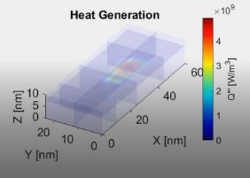
The dominant energy carriers associated with the movement of thermal energy in materials like silicon are called phonons. Phonons are related to the energy that is transported as a result of the presence of atomic lattice vibrational waves. The atoms of solids are arranged in a regular repeating way within a material and this is referred to as the lattice. The atoms vibrate about the equilibrium positions and with this vibration they effect neighboring atoms. The vibrational energy is transmitted between different regions of the material in the form of a wave. These vibrational waves are similar in nature to waves on a string (transverse waves) or sound waves (longitudinal or compression). However, the quantum nature of matter dictates that everything is both a wave and a particle. Thus, the energy (and momentum) of the lattice vibrational waves can be pictured as the movement of particle. It is this particle that we call the phonon. Phonons are to solids as photons (packets of energy) are to light. As phonons move through the material, they can interact with other phonons, boundaries, impurities, interfaces, photons, and (of most importance for heat generation) moving electrons. The relative ease with which they can be transported from one region to the other will dictate “how hot” any particular spot becomes. In addition, the nature of the phonons in any given region can affect the overall performance of the transistor.
This detailed information is important to know and useful to designers. This is where I come in (enter stage left). I develop computer programs to predict phonon transport in transistors (funny right, using a computer to predict what is happening in a computer). Methods to model phonon transport do exist, however they lack in the right combination of accuracy, flexibility, and efficiency. I am working toward the goal of developing a program that meets all of the above criteria. Device based design models have to strike the right balance between the above factors in order to both provide useful insight into phonon transport phenomena and be able to be used to perform parametric studies or sensitivities to design parameters. It is the hope that designers will use the information and insight gained to change key design characteristics for thermal considerations. This could be the geometric layout (like fin dimensions and spacing), operating characteristics (current and voltage), or the use of enhanced heat transfer materials that lead to reduced hot spots, faster performance, and increased reliability.
With a little luck, the future might not be quite as hot for transistors and CPU’s with the aid of phonon transport modeling. So, the next time you pick up your phone, start up your laptop, or put on your smart watch remember the phenomena that occur on the smallest length scales and shortest time scales can be very important. q
Michael P. Medlar is a PhD student in Engineering and a Senior Lecturer at RIT. Prior to his work at RIT, he spent 7 ½ years at Knolls Atomic Power Laboratory in Niskayuna, NY. Medlar graduated with a BS/MS in Mechanical Engineering from RIT in 2003.


