
8 minute read
MIRTEC


MIRTEC Interview with Brian D’Amico

An award-winning leader in inspection technology, MIRTEC is committed to continuous improvement through innovation and quality. The company’s inspection solutions have helped thousands of electronics manufacturing companies maximize their profitability by promoting unparalleled levels of quality and efficiency within the manufacturing process. MIRTEC is constantly moving, adapting and creating in order to stay at the forefront of technology and to help its customers stay at the top of their industries. We recently spoke with Brian D’Amico, President of MIRTEC Corp., to find out more about the company’s business philosophy and latest innovations.
Industry 4.0 and Smart Factory Automation are becoming more important within the Electronics Manufacturing Industry. Can you briefly explain the benefits of Smart Factory Automation and MIRTEC’s role?
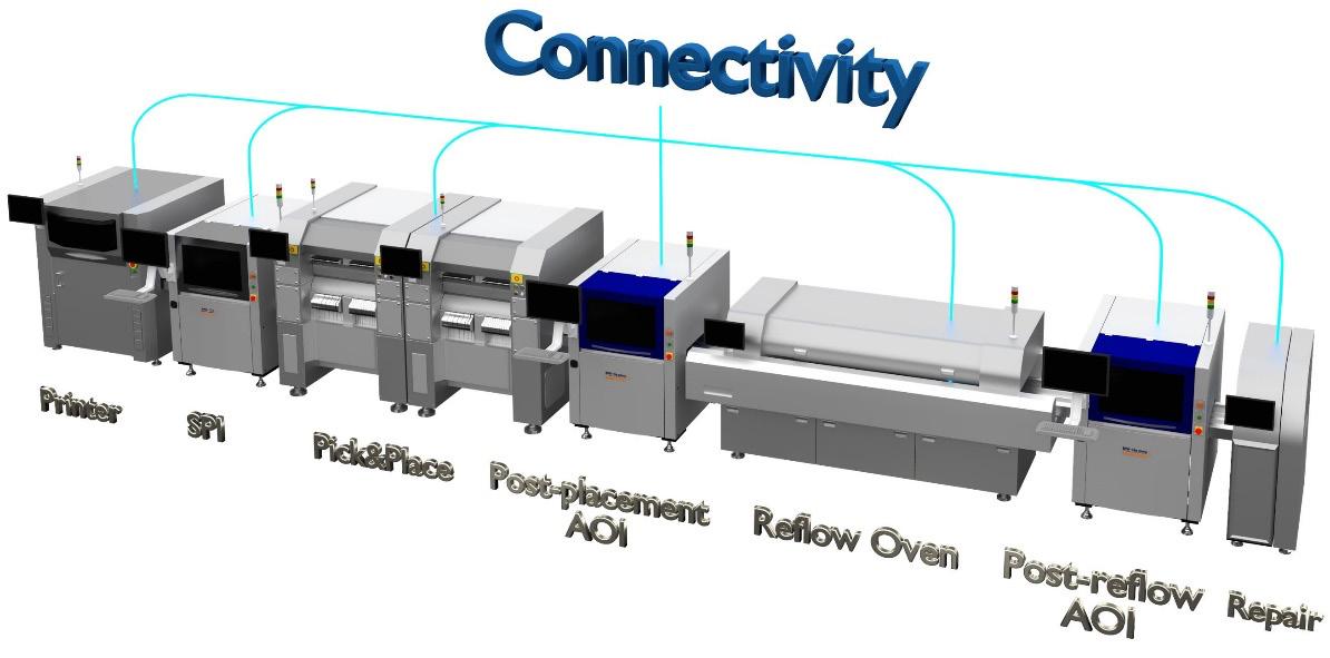
Certainly. In the most simplistic of terms, Industry 4.0 is a trend toward automation and data exchange within the manufacturing process. Therefore, Smart Factory Automation is an integral part of Industry 4.0. With respect to electronics manufacturing, this basically requires connectivity and machineto-machine (M2M) communication within the manufacturing line. The challenge is to collect data from each of the systems within the line and make that data available to the rest of the machines. Without test and inspection, there is no Industry 4.0. This is where MIRTEC comes into play. The whole purpose of test and inspection is to collect actionable data that may be used to reduce defects and maximize efficiency within the manufacturing line. The goal is to minimize scrap and get a good handle on those process parameters that need to be put in place to manufacture products the right way the first time.
For maximum efficiency, three inspection systems are required within the production line. These are solder paste inspection (SPI) post-solder deposition, automated optical inspection (AOI) post-placement and AOI post-reflow. This requires a substantial investment; however, the combination of all three inspection machines is really the only true way to provide feedback for each stage of the manufacturing process.
If I understand correctly, you are recommending three inspection systems within each manufacturing line. This seems like a break from the traditional thought of using one inspection machine post- reflow. Can you please explain the reason for the additional inspection systems and the benefits of feedback within the line?
Absolutely. While I understand and agree that most manufacturers rely upon a single post-reflow AOI system, the problem is that it becomes more difficult to diagnose and resolve where an issue may have occurred within the manufacturing line because we are only looking at a snapshot of the final result of all the other assembly equipment within the line. From there, we are basically making an ‘educated guess’ as to where the issue occurred.
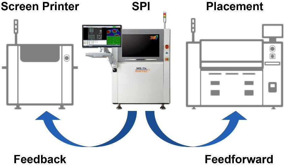
The introduction of an SPI system, for example, would provide immediate feedback of issues such as insufficient or excessive solder, solder bridging or solder offset directly after solder deposition. These issues are typically related to process parameters such as stroke speed, for a screen printer, squeegee pressure, under-stencil cleaning etc. The bottom line is that it is more difficult to diagnose screen printing issues based on data collected by post reflow AOI.
Closed-loop feedback provides a means of reporting inspection data back to the screen printer, which may then be used to adjust certain parameters to effectively eliminate the possibility of future defects. Adjustments are typically made based on trends within the inspection data. For example, let’s say that the SPI machine detects an offset trend in solder depositions with respect to pad location. Under these circumstances the SPI machine would report the trend to the Screen Printer. The screen printer, in turn, may use this data to adjust the location of the stencil with respect to the pads in order to eliminate the offset. However, this depends upon the level of sophistication of the screen printer to accept this data and then make the necessary changes to the specified parameters to resolve the issue. Please keep in mind that the goal is not to control the screen printer, but to provide actionable data that may be used to eliminate the offset trend and potential defects.
As previously mentioned, it is difficult to determine which adjustments need to occur throughout the line based on post-reflow analysis of defect data. One can certainly make assumptions, but those assumptions are so far down the line that it becomes increasingly difficult to determine exactly where the defect occurred. From the customer’s perspective, I completely understand that we are suggesting a substantial investment in test equipment, however, the absolute best way to get a handle on the entire production line is to have testing at each interval within the line; post-solder deposition, postplacement and post-reflow. That is really what Smart Factory Automation is all about.
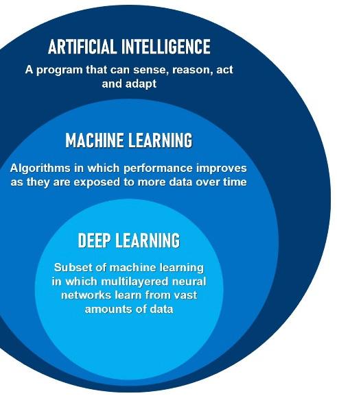
There is much discussion regarding the adoption of artificial intelligence (AI) within the electronics manufacturing environment. We understand that MIRTEC has been a pioneer in this regard. Can you please provide a better understanding of the benefits of MIRTEC’s AIbased smart factory solutions?
My pleasure. In recent years, 3D AOI machines have developed rapidly, and many new functions have been added. While these performance improvements are welcome, they have added another level of complexity to the programming and optimization of the inspection system. 3D AOI machines require much more parameter manipulation for teaching and debugging resulting in increased dependency on the skill of the process engineer. This presents a host of new challenges. If a skilled employee is replaced or a new employee is introduced due to the addition of more SMT lines, productivity may be adversely affected until the skill level of the employee is improved. Such uncertainty and instability are something that electronics manufacturers must avoid in order to maintain quality control. This is where the
need for AI is highlighted. In short, the goal of using AI is to reduce dependency on the level of operator proficiency required to maintain the highest levels of manufacturing quality and efficiency.
An essential part of a connected Smart Factory is the collection of what is referred to as Big Data. By applying a subset of AI called Deep Learning Analytics to this Big Data we can determine the optimal process parameters for maximum quality and efficiency. When setting up a new PCB, an SMT engineer will program the process parameters for each system within the manufacturing line based on the respective experience of the engineer. Deep Learning Methodology is designed to assist with this daunting task of process optimization by predicting optimal parameters based on historical data. The goal is to achieve the highest production quality regardless of the capability or experience of the engineer.
The performance of the line must then be monitored in real-time through continuous collection and analysis of production data.
We understand that Process Optimization is a key benefit of Smart Factory Automation, but where do humans fit in? Is the goal to completely eliminate human interaction within the manufacturing process?
No. From my perspective there is really no substitute for a good process engineer as he or she will have the experience and know-how to make a production line ‘sing.’ In setting up the screen printer, for instance, a good engineer may recognize that a step-stencil may require certain squeegee speed and pressure for optimal solder deposition. He or she may also know how to tune the pick-and-place machine for optimal performance. For example, there may be certain devices that require a bit more pressure or dwell time during placement. The same is true in developing optimal reflow profiles as well. The key here is that this requires a level of expertise as a result of having spent a lot of time working with a given production line and knowing the nuances of each machine. The whole purpose of having machine-to-machine connectivity and communication is to collect and analyze process data and provide optimal parameters for each machine within the line thereby removing much of the ‘artfulness: in the manufacturing process. Furthermore, a complete Smart Factory Solution will monitor each phase of the production line in real-time so as to maintain maximum quality and efficiency throughout the manufacturing process.
MIRTEC is well known for product innovation. Has MIRTEC introduced any new products recently that you would like to share with our readers?
What would you like the electronics manufacturing industry to know about MIRTEC?
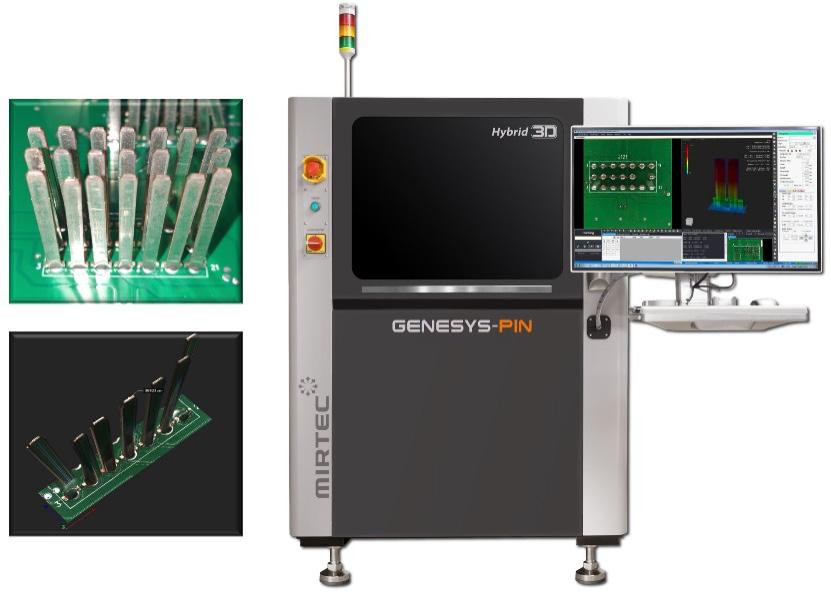
Yes, at IPC APEX EXPO this year MIRTEC debuted a new system specifically designed for the automotive electronics market, MIRTEC’s GENESYS-PIN Hybrid 3D Inspection System. The revolutionary optical system of the GENESYS-PIN machine is capable of measuring automotive connector pins up to 50 mm tall with extreme accuracy. The machine is configured with a 12 Megapixel CoaXPress High-speed Camera System, a 15 µm Precision Telecentric Lens, an advanced 9 Phase RGB Color Lighting System, Programmable Multi-Focus Z-Axis System, and four Programmable Multi-Pattern Digital Projectors that are an integral part of MIRTEC’s proprietary Hybrid 3D Measurement Technology. The GENESYSPIN machine detects defects such as missing pins, pin offset, distance between pins and inner/outer dimensions of forked pins, ensuring that automotive PCBs are manufactured to the highest quality standards.
With more than 17,000 systems installed throughout the world and having received a total of 45 industry awards for our products and services thus far, MIRTEC has earned a solid reputation as one of the most progressive and dynamic suppliers of automated inspection equipment to the electronics manufacturing industry. MIRTEC products have been extremely successful in both high-volume/low-mix consumer electronics manufacturing as well as low- to medium-volume/high-mix, high-complexity medical, automotive, aerospace and defense manufacturing environments. With a total of 12 centers of excellence and more than 60 sales and support centers located strategically throughout the world, MIRTEC provides a full range of services including consultation, installation, equipment training, and after-sales support.
Ours is a business of precision and accuracy, reproducibility and specificity, timeliness, and trust. These are the real products and services that we provide to our valued customers. We welcome the opportunity to demonstrate how MIRTEC’s technologically advanced inspection solutions can help your business achieve the highest levels of quality, efficiency, and profitability.
Thank you for the opportunity to share this information with your readers!


