OPTICAL ANTENNAS FOR COMPUTER CHIPS


OPTICAL ANTENNAS FOR COMPUTER CHIPS


EARTHQUAKE ON A CHIP FLEXIBLE, TUNEABLE ANTENNAS





Welcome to the final issue of What’s New in Electronics for 2024!

It has been a tumultuous year for the global electronics industry, compounded by the results of the US Presidential election. As President-elect Donald Trump prepares to return to the White House, the Biden Administration is under pressure to finalise deals that were made under the 2022 CHIPS and Science Act, which aimed to strengthen semiconductor manufacturing in the US with $39 billion in grants. Donald Trump has previously criticised the bipartisan Act, proposing to institute more tariffs instead.
Despite all this, the latest forecast from Gartner, Inc. indicates that global semiconductor revenue is projected to grow 14% in 2025 to total $717 billion, driven by a surge in AI-related semiconductor demand and recovery in electronic production. The memory market and graphics processing units (GPUs) are also forecast to bolster semiconductor revenue globally, with the worldwide memory revenue market to record 20.5% growth in 2025, to total $196.3 billion. All this to say, 2025 is shaping up to be an interesting year and What’s New in Electronics will be here to share insights about new research and developments in the global electronics industry.
This issue’s lead article covers the development of a silent amplifier and recordsensitive receiver that could pave the way for faster and improved space communication. While networks and communication systems are one of the key features of this issue, the magazine also includes articles about a nanometre-sized light antenna with electrically modulated surface properties that could enable the production of faster computer chips, along with an insightful article from Drexel University about the use of kirigami — a version of origami — to create tuneable radio antennas.
I hope you enjoy this issue of the magazine. If you would like to contribute an article or a case study, or have feedback to share, please contact: wnie@ wfmedia.com.au.
Wishing you all a fun, safe and relaxing festive season!
Ashna Mehta Editor

In space exploration, long-distance optical links can now be used to transmit images, films and data from space probes to Earth using light. But in order for the signals to reach all the way and not be disturbed along the way, hypersensitive receivers and noise-free amplifiers are required.
Now, researchers at Chalmers University of Technology, in Sweden, have created a system that, with a silent amplifier and record-sensitive receiver, paves the way for faster and improved space communication.
Space communication systems are increasingly based on optical laser beams rather than radio waves, as the signal loss has been shown to be less when light is used to carry information over very long distances. But even information carried by light loses its power during the journey, and optical systems for space communication therefore require extremely sensitive receivers capable of sensing signals that have been greatly weakened before they finally reach Earth. The Chalmers researchers’ concept for optical space communication opens up new communication opportunities — and discoveries — in space.
“We can demonstrate a new system for optical communication with a receiver that is more sensitive than has been demonstrated previously at high data rates. This means that you can get a faster and more error-free transfer of information over very long distances, for example when you want to send high-resolution images or videos from the Moon or Mars to Earth,” says Peter Andrekson, Professor of Photonics at Chalmers and one of the lead authors of the study, which was recently published in the scientific journal Optica.
The researchers’ communication system uses an optical amplifier in the receiver that amplifies the signal with the least possible noise so that its information can be recycled. Just like the glow of a flashlight, the light from

In the new communication system from researchers at Chalmers University of Technology, in Sweden, a weak optical signal (red) from the spacecraft’s transmitter can be amplified noisefree when it encounters two so-called pump waves (blue and green) of different frequencies in a receiver on Earth. Thanks to the researchers’ noise-free amplifiers in the receiver, the signal is kept undisturbed and the reception on Earth becomes record-sensitive, which in turn paves the way for a more error-free and faster data transmission in space in the future.
the transmitter widens and weakens with distance. Without amplification, the signal is so weak after the space flight that it is drowned out by the electronic noise of the receiver. After 20 years of struggling with disturbing noise that impaired the signals, the research team at Chalmers was able to demonstrate a noise-free optical amplifier a few years ago. But until now, the silent amplifier has not been able to be used practically in optical communication links, as it has placed completely new, significantly more complex, demands on both transmitter and receiver.
Due to the limited resources and minimal space on board a space probe, it is important that the transmitter is as simple as possible. By allowing the receiver on Earth to generate two of the three light frequencies needed for noise-free amplification, and at the same time allowing the transmitter to generate only one frequency, the Chalmers researchers were able to implement the noise-free amplifier in an optical communication system for the first time. The results show an outstanding sensitivity, while complexity at the transmitter is modest.
“This phase-sensitive optical amplifier does not, in principle, generate any extra noise, which contributes to a more sensitive receiver and that error-free data transmission is achieved even when the power of the signal is lower. By generating two extra waves of different frequencies in the receiver, rather

than as previously done in the transmitter, a conventional laser transmitter with one wave can now be used to implement the amplifier. Our simplification of the transmitter means that already existing optical transmitters on board satellites and probes could be used together with the noise-free amplifier in a receiver on Earth,” says Rasmus Larsson, Postdoctoral Researcher in Photonics at Chalmers and one of the lead authors of the study.
The progress means that the researchers’ silent amplifiers can eventually be used in practice in communication links between space and Earth. The system is thus poised to contribute in solving a well-known bottleneck problem among space agencies today.
“NASA talks about ‘the science return bottleneck’, and here the speed of the collection of scientific data from space to Earth is a factor that constitutes an obstacle in the chain. We believe that our system is an important step forward towards a practical solution that can resolve this bottleneck,” says Peter Andrekson.
The next step for the researchers is to test the optical communication system with the implemented amplifier during field studies on Earth, and later also in communication links between a satellite and Earth.

University of Würzburg
Today’s computers reach their physical limits when it comes to speed. Semiconductor components usually operate at a maximum usable frequency of a few gigahertz — which corresponds to several billion computing operations per second. As a result, modern systems rely on several chips to divide up the computing tasks because the speed of the individual chips cannot be increased any further. However, if light (photons) were used instead of electricity (electrons) in computer chips, they could be up to 1000 times faster.
Plasmonic resonators, also known as “antennas for light”, are a promising way of achieving this leap in speed. These are nanometre-sized metal structures in which light and electrons interact. Depending on their geometry, they can interact with different light frequencies.
“The challenge is that plasmonic resonators cannot yet be effectively modulated, as is the case with transistors in conventional electronics. This hinders the development of fast light-based switches,” said Dr Thorsten Feichtner, physicist at Julius-Maximilians-Universität (JMU) Würzburg in Bavaria, Germany.
Charged optical antennas: University of Würzburg breaks new ground
A JMU research team in collaboration with the Southern Denmark University (SDU) in Odense has now taken a significant step forward in the modulation of light antennas: It has succeeded in achieving electrically controlled modulation that points the way to ultra-fast active plasmonics and thus to significantly faster computer chips. The experiments have been published in the journal Science Advances.
Instead of trying to change the entire resonator, the team focused on changing its surface properties. This breakthrough was achieved by electrically contacting a single resonator, a nanorod made of gold — an idea that is conceptually simple, but could only be realised with the help of sophisticated nanofabrication based on helium ion beams and gold nanocrystals. This unique fabrication method has been established at the JMU Chair of Experimental Physics (Biophysics) under the direction of Professor Bert Hecht. Sophisticated measurement techniques with a lock-in amplifier were crucial for detecting the small but significant effects on the surface of the resonator.
Study leader Feichtner said, “The effect we are making use of is comparable to the principle of the Faraday cage. Just as the electrons in a car struck by lightning collect on the outside and the occupants inside are safe, additional electrons on the surface influence the optical properties of the resonators.”
Until now, optical antennas could almost always be described classically: the electrons of the metal simply stop at the edge of the

nanoparticle, like water at a harbour wall. However, the measurements taken by the Würzburg scientists revealed changes in the resonance that can no longer be explained in classical terms: the electrons ‘smear’ across the boundary between metal and air, resulting in a soft, graduated transition, similar to a sandy beach met by the sea.
To explain these quantum effects, theorists at SDU Odense developed a semi-classical model. It incorporates the quantum properties into a surface parameter so that the calculations can be carried out using classical methods. “By perturbing the response functions of the surface, we combine classical and quantum effects, creating a unified framework that advances our understanding of surface effects,” explained JMU physicist Luka Zurak, first author of the study.
The new model can reproduce the experiments, but exactly which of the many quantum effects are involved at the metal surface is not clear at the moment. “But with this study, it is now possible for the first time to specifically design new antennas and exclude or amplify individual quantum effects,” Feichtner said.
In the long term, the researchers envisage even more applications: smaller resonators promise optical modulators with high efficiency, which could be used technologically. In addition, the influence of surface electrons in catalytic processes can also be investigated with the system presented. This would provide new insights into energy conversion and energy storage technologies.
The research findings have been published in the journal Science Advances.

Advancements in quantum information technology are paving the way for more efficient data transfer. A key challenge has been ensuring that qubits, the units of quantum information, can be transferred between different wavelengths without losing their essential properties, such as coherence and entanglement.
Now, researchers from Shanghai Jiao Tong University (SJTU) have developed a method for broadband frequency conversion, marking a step forward for future quantum networks. The SJTU team focused on a technique using X-cut thin film lithium niobate (TFLN), a material known for its nonlinear optical properties. The researchers achieved second-harmonic generation — an important process for converting light from one wavelength to another — with a bandwidth of up to 13 nanometres. This was accomplished through a process called mode hybridisation, which allows for
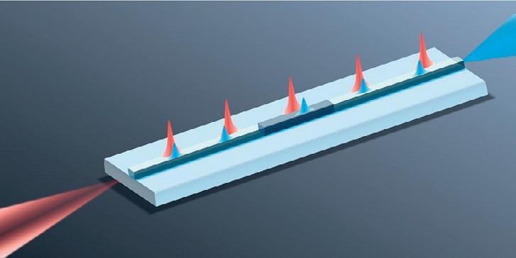
Dispersion-designed structural geometry enables groupvelocity mismatch of interacting lights to be smoothed to zero, for wide-range frequency conversion.
precise control over the frequency conversion in a micro-racetrack resonator.
Corresponding author Yuping Chen said an efficient second-order nonlinear process with widely tuneable pump bandwidth has been a long-pursued goal, due to the extensive applications in wavelength division multiplexing networks, ultrashort pulse nonlinearity, quantum key distribution and broadband single-photon source generation.
“Thanks to the great progress in fabrication technology on the TFLN platform, this work will pave the way to chip-scale nonlinear frequency conversion between the ultrashort optical pulses and even the quantum states,” Chen said.
The research findings could have wide-ranging implications for integrated photonic systems. By enabling on-chip tuneable frequency conversion, the new method opens the door to enhanced quantum light sources, larger capacity multiplexing and more effective multichannel optical information processing.

From brighter TV screens to better medical diagnostics and more efficient solar panels, new Curtin-led research has discovered how to make more molecules stick to the surface of tiny nanocrystals, in a breakthrough that could lead to improvements in everyday technology.
Lead author Associate Professor Guohua Jia from Curtin’s School of Molecular and Life Sciences, said the study investigated how the shape of zinc sulfide nanocrystals affected how well molecules, known as ligands, stick to their surface.
“Ligands play a key role in controlling the behaviour and performance of zinc sulfide nanocrystals in various important technologies,” Jia said.
“In a discovery that could open new possibilities for developing smarter, more advanced devices, our study found flatter, more even particles called nanoplatelets allow more ligands to attach tightly, compared to other shapes like nanodots and nanorods.
“By adjusting the shape of these particles, we were able to control how they interacted with their surroundings and make them more efficient in various applications.
“From brighter LED lights and screens to more efficient solar panels and more detailed medical imaging, the ability to control particle shapes could revolutionise product efficiency and performance.”
Jia said the discovery could enhance the performance of devices known as optoelectronics, which either produce light or use light to perform their functions.
“Optoelectronics are important in many modern technologies, including telecommunications, medical devices and energy production,” Jia said.
“The ability to efficiently manipulate light and electricity is central to the advancement of faster, more efficient and more compact electronic systems.
“This includes LEDs, which convert electricity into light and are used in everything from light bulbs to TV screens as well as solar cells that convert light into electrical energy, powering devices using sunlight.
“Other devices that could be advanced by this discovery include photodetectors that sense light and convert it into an electrical signal, such as in cameras and sensors, plus laser diodes used in fibreoptic communication that convert electrical signals into light for data transmission.”
The research findings have been published in the Journal of the American Chemical Society.

Researchers have demonstrated a total output power of more than 8 W from a high-power mid-infrared (mid-IR) cadmium silicon diphosphide (CSP) optical parametric oscillator (OPO) pumped at 2.06 µm. The researchers showed that CSP crystals can out-perform zinc germanium phosphide (ZGP) for frequency down-conversion from 2 microns to the mid-IR band. This high-power mid-IR output could be useful for infrared spectroscopy, laser surgery, remote sensing and defence communications.
Marcin Piotrowski from the French-German Research Institute in France of Saint Louis led this research project and said that laser power scaling in this spectral band is important for infrared countermeasures in defence — protecting aircraft and other platforms from the threat of infrared-seeking missiles. “Efficient sources capable of delivering high power with good beam quality are critical, as the laser beam must travel long distances through the atmosphere,” Piotrowski said.
CSP crystals are a promising alternative to ZGP for frequency conversion in OPOs. However, few studies have examined CSP for parametric conversion with pump wavelengths that are longer than one micron. In this study, the researchers focused the pump laser to a 1-mm diameter spot inside an OPO resonator formed by two flat mirrors. The CSP sample was nine millimetres long with a 4 x 4 mm2 aperture. A ZGP sample of the same size was also used for comparison.
Although the conversion threshold for the two materials was different, CSP demonstrated a better conversion efficiency for high pump power. The absorption properties of ZGP also caused thermal effects to become more significant. The researchers found that CSP had a lower thermal load and less beam degradation while ZGP showed reduced beam quality at high powers due to higher residual absorption.
These experimental results suggest that CSP crystals may outperform ZGP for frequency down-conversion from 2 µm to the mid-IR range.
“We look forward to continuing our investigations on nonlinear crystals such as CSP for OPO emission in the mid-IR. In particular, as the quality and maturity of the CSP material allows, we will combine it with the technologies actively investigated in our research group: monolithic non-planar cavities such as the FIRE cavity — particularly well suited for power scaling while maintaining good beam quality. In addition, compact and robust 2 µm fibre lasers are planned as future pump sources for these OPO cavities,” Piotrowski said.


Researchers from the Pohang University of Science and Technology (POSTECH) have enhanced the commercial viability of spin wave harnessing technology. This development could present a next-generation technological solution to the issue of heat generation in electronic devices. The research findings were published in the journal Matter
When devices such as smartphones and computers heat up, it is due to the movement of electrons within the device as they store and process data, causing some energy to convert into heat. With the rapid advancement of artificial intelligence and cloud computing, electronics are becoming smaller and more complex, intensifying the overheating problem.
One way to solve the problem of heat generation in electronic devices is by using ‘spin waves’ in information transmission
The transition to renewable energy requires efficient methods for storing large amounts of electricity. Researchers at the Technical University of Munich (TUM) have developed a new method that could extend the lifespan of aqueous zinc-ion batteries by several orders of magnitude. Instead of lasting just a few thousand cycles, they could now endure several hundred thousand charge and discharge cycles.
The key to this innovation is a special protective layer for the zinc anodes of the batteries. This layer addresses previous issues such as the growth of needle-like zinc structures — known as zinc dendrites — as well as unwanted chemical side reactions that trigger hydrogen formation and corrosion.
The research team, led by Professor Roland A. Fischer, Chair of Inorganic and Metal-Organic Chemistry at the TUM School of Natural Sciences, uses a unique material for this purpose: a porous organic polymer called TpBD-2F. This material forms a stable, ultra-thin, and highly ordered film on the zinc anode, allowing zinc ions to flow efficiently through nano-channels while keeping water away from the anode.
Zinc batteries as a cost-effective alternative to lithium-ion batteries
Da Lei, PhD student and lead author of the research published in Advanced Energy Materials, explains: “Zinc-ion batteries
technology. Spin waves are waves that can transmit information without the flow of electrons by utilising the spin characteristics of electrons in magnetic insulators. Research has shown that increasing the temperature imbalance of spin waves in a material — for example, due to the tendency of spin waves on one side of the material to become hotter and the other side to become colder — increases the informationcarrying efficiency of spin waves. However, there is no technology that can independently control the temperature of spin waves.
The researchers from POSTECH have developed a novel approach, inspired by the radiator fins used to cool automobile engines. The researchers incorporated nanometre-scale gold structures at one end of a thin film made of magnetic insulator, designing it to effectively regulate temperature based on the concentration of the gold. These gold structures reduced the temperature of the spin waves at the targeted location, creating a temperature imbalance within the material.
The experiments demonstrated that this thin film reportedly improved spin wave transfer efficiency by 250% compared to conventional methods. The researchers reported the successful independent control of spin wave temperature and demonstrated a method for enhancing spin wave transfer efficiency by utilising this control.
Professor Hyungyu Jin from POSTECG said this research represents a significant milestone in developing next-generation information transfer technologies to address heat generation in electronics. Dr Sang Jun Park, the study’s lead author, said “By overcoming previous limitations, this technology has promising potential for a wide range of future applications using spin waves.”

with this new protective layer could replace lithium-ion batteries in large-scale energy storage applications, such as in combination with solar or wind power plants. They last longer, are safer, and zinc is both cheaper and more readily available than lithium.” While lithium remains the first choice for mobile applications like electric vehicles and portable devices, its higher costs and environmental impact make it less attractive for large-scale energy storage.
Fischer adds: “This is truly a spectacular research result. We have shown that the chemical approach developed by Da Lei not only works but is also controllable. As fundamental researchers, we are primarily interested in new scientific principles — and here we have discovered one. We have already developed a first prototype in the form of a button cell. I see no reason why our findings couldn’t be translated to larger applications. Now, it’s up to engineers to take up the idea and develop appropriate production processes.”

University College London
A new world record in wireless transmission, promising faster and more reliable wireless communications, has been set by researchers from UCL.
The team successfully sent data over the air at a speed of 938 Gigabits per second (Gb/s) over a record frequency range of 5–150 Gigahertz (GHz).
This speed is up to 9380 times faster than the best average 5G download speed in the UK, which is currently 100 Megabits per second (Mb/s) or over. The total bandwidth of 145 GHz is more than five times higher than the previous wireless transmission world record.
Typically, wireless networks transmit information using radio waves over a narrow range of frequencies. Current wireless transmission methods, such as Wi-Fi and 5G mobile, predominantly operate at low frequencies below 6 GHz.
But congestion in this frequency range has limited the speed of wireless communications.
Researchers from UCL Electronic & Electrical Engineering overcame this bottleneck by transmitting information through a much wider range of radio frequencies by combining both radio and optical technologies for the first time. The results are described in a new study published in The Journal of Lightwave Technology
This more efficient use of the wireless spectrum is expected to help meet growing demand for wireless data capacity and speed over the next three to five years.
Dr Zhixin Liu, senior author of the study from UCL Electronic & Electrical Engineering, said: “Current wireless communication systems are struggling to keep up with the increasing demand for high-speed data access, with capacity in the last few metres between the user and the fibre optic network holding us back.
“Our solution is to use more of the available frequencies to increase bandwidth, while maintaining high signal quality and providing flexibility in accessing different frequency resources. This results in super-fast and reliable wireless networks, overcoming the speed bottleneck between user terminals and the Internet.
“Our new approach combines two existing wireless technologies for the first time, high-speed electronics and millimetre wave photonics, to overcoming these barriers. This new system allows for the transmission of large amounts of data at unprecedented speeds, which will be crucial for the future of wireless communications.”
To address the current limitations of wireless technology, researchers from UCL developed a novel approach that combines advanced electronics, which performs well in the 5–50 GHz range, and a technology called photonics that uses light to generate radio information, which performs well in the 50–150 GHz range.

The team generated high-quality signals by combining electronic digital-to-analogue signal generators with light-based radio signal generators, allowing data to be transmitted across a wide range of frequencies from 5–150 GHz.
State-of-the-art communications networks rely on several technologies to function. Optical fibre communications systems transmit data over long distances, between continents and from data centres to people’s homes. Wireless technology often comes in at the final stage, when data is transmitted a short distance, for example from a household internet router to the devices connected to it over Wi-Fi.
While optical fibre, which forms the backbone of modern communications networks, has made big advances in bandwidth and speed in recent years, these gains are limited without similar advances in the wireless technology that transmits information the final few metres in homes, workplaces and public spaces around the world.
The new UCL-developed technology has the potential to revolutionise various sectors, not least the Wi-Fi connectivity that people rely on at home and in other public places.
Mobile phone users can expect faster mobile internet speeds and more stable connections, with 5G and later 6G networks powered by this type of system. This would allow more people to use the network in densely populated urban environments or at large event like concerts without experiencing slowdown, or provide the same number of users with much faster speeds.
For example, a two-hour 4K Ultra HD film (around 14 GB of data) would take 19 minutes to download over 5G at 100 Mb/s. Using the new technology it could be downloaded in just 0.12 seconds.
Professor Izzat Darwazeh, an author of the study and director of UCL Institute of Communications and Connected Systems (ICCS) from UCL Electronic & Electrical Engineering, said: “The beauty of wireless technology is its flexibility in terms of space and location. It can be used in scenarios where optical cabling would be challenging, such as in a factory containing complex arrangements of equipment.
“This work brings wireless technology up to speed with the increased bandwidths and speeds that have been achieved with the radio frequency and optical communications systems within next-generation digital communications infrastructure.”
While the technology has only currently been demonstrated in the laboratory, work is underway to produce a prototype system that can be used for commercial testing. If this is successful, the technology will be ready to incorporate into commercial equipment within three to five years.
Professor Polina Bayvel, an author of the study, co-director of ICCS and Head of the UCL Optical Networks Group, said: “We are grateful to UKRI and the EPSRC for supporting this work to enable us to establish worldleading testbed and experimental capabilities in these areas. They are essential for the future of the UK’s national communications infrastructure, which is a critical resource.”
This is a modified version of a news item published by University College London.
The Advantech MIC-770 V3 Extreme SKU is a compact, modular IPC designed to provide enhanced performance in environments where traditional airflowbased cooling systems are not feasible. Featuring the latest 12/13/14th Gen Intel Core processors, the fanless edge computer is designed to provide exceptional computing power to handle demanding multitasking workloads, such as factory automation, machinery control and process automation.
With Advantech’s advanced thermal solution, it is capable of operating at up to 35°C with a 65 W CPU, and up to 50°C with a 35 W CPU. This innovative design enables stable performance in extreme environments that lack airflow, maintaining optimal CPU functionality — crucial for machine vision and automation inspection tasks.
The system also supports Windows 11, including Windows 11 IoT Enterprise LTSC with 10-year support and enhanced security, offering easy management and system protection. These features make the MIC-770 V3 Extreme SKU a powerful platform with rich I/O options and multiple display options suited for a variety of industrial environments.
Advantech’s MIC-770 V3 Extreme SKU, MIC-770V3W-E0A1 and MIC-770V3H-E0A1 are available now. Advantech Australia Pty Ltd
www.advantech.net.au

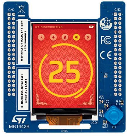
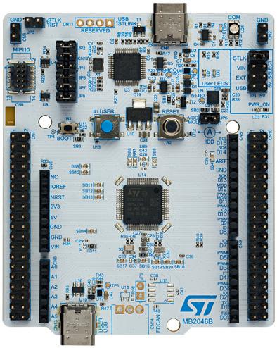
The STM32C071 graphical user interface has enhanced the memory configuration of the STM32C031 thanks to 128 KB of flash and 24 KB of RAM.
The device is still available in the same TSSOP20 package (6.5 x 4.4 mm), while providing more complex applications in spaceconstrained USB peripherals for PCs.
The STM32C071 also has the ability to drive UIs that previously required more expensive devices. The device is designed to bring more functionalities and capabilities from the STM32G0 down to the STM32C0. Besides the USB controller, the additional SPI and the I2C interface, users also get a 32-bit timer.
The STM32C071 is a new roadmap enabler as it bridges the gap between entry-level MCUs and the STM32G0 that teams must use to provide the same feature-set to their customers. The pin-out is compatible between the STM32C071 and the STM32G0 and STMicroelectronics now offers a new 64-pin package for the new STM32C0. STMicroelectronics Pty Ltd www.st.com
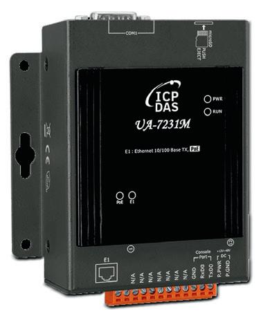
The ICP DAS UA-7231M is an Industrial IoT (IIoT) communication server designed to bridge the gap between IT and OT systems in industrial environments. Housed in a sturdy metal case, it features a Power over Ethernet (PoE) port and a serial port for versatile connectivity.
Another feature of the IIoT communication server is its ability to simultaneously support OPC UA and MQTT protocols, providing a flexible communication solution. It comes with an integrated MQTT broker, including WebSocket support, to facilitate seamless data exchange. The server also incorporates a range of security measures, such as HTTPS communication encryption and blocklist functions, safeguarding data integrity.
The product serves as an IIoT gateway, enabling remote access to I/O modules and controllers using Modbus TCP/ RTU/ASCII, MQTT and EtherNet/IP. It can convert these I/O data into OPC UA or MQTT protocols, making them compatible with systems like MES, ERP, SCADA and cloud services. The data logger function allows direct writing of I/O data into remote databases and local storage for historical records.
Compatible with leading cloud platforms like Microsoft Azure, AWS and IBM Bluemix, and supporting IFTTT logic for app notifications, the device is designed to simplify IIoT deployment, enhancing operational efficiency.
ICP Electronics Australia www.icp-australia.com.au

Adam Zewe, MIT

Silicon transistors, which are used to amplify and switch signals, are a critical component in most electronic devices, from smartphones to automobiles. But silicon semiconductor technology is held back by a fundamental physical limit that prevents transistors from operating below a certain voltage.
This limit, known as “Boltzmann tyranny”, hinders the energy efficiency of computers and other electronics, especially with the rapid development of artificial intelligence technologies that demand faster computation.
In an effort to overcome this fundamental limit of silicon, MIT researchers fabricated a different type of three-dimensional transistor using a unique set of ultrathin semiconductor materials.
Their devices, featuring vertical nanowires only a few nanometres wide, can deliver performance comparable to state-of-the-art silicon transistors while operating efficiently at much lower voltages than conventional devices.
“This is a technology with the potential to replace silicon, so you could use it with all the functions that silicon currently has, but with much better energy efficiency,” said Yanjie Shao, an MIT postdoc and lead author of a paper on the new transistors.
The transistors leverage quantum mechanical properties to simultaneously achieve low-voltage operation and high performance within an area of just a few square nanometres. Their extremely small size would enable more of these 3D transistors to be packed
onto a computer chip, resulting in fast, powerful electronics that are also more energy-efficient.
“With conventional physics, there is only so far you can go. The work of Shao shows that we can do better than that, but we have to use different physics. There are many challenges yet to be overcome for this approach to be commercial in the future, but conceptually, it really is a breakthrough,” said senior author Jesús del Alamo, the Donner Professor of Engineering in the MIT Department of Electrical Engineering and Computer Science (EECS).
They are joined on the paper by Ju Li, the Tokyo Electric Power Company Professor in Nuclear Engineering and professor of materials science and engineering at MIT; EECS graduate student Hao Tang; MIT postdoc Baoming Wang; and professors Marco Pala and David Esseni of the University of Udine in Italy. The research was published in Nature Electronics
In electronic devices, silicon transistors often operate as switches. Applying a voltage to the transistor causes electrons to move over
THIS IS A TECHNOLOGY WITH THE POTENTIAL TO REPLACE SILICON. — YANJIE SHAO

iStock.com/NatalyaBurova
an energy barrier from one side to the other, switching the transistor from “off” to “on”. By switching, transistors represent binary digits to perform computation.
A transistor’s switching slope reflects the sharpness of the “off” to “on” transition. The steeper the slope, the less voltage is needed to turn on the transistor and the greater its energy efficiency.
But because of how electrons move across an energy barrier, Boltzmann tyranny requires a certain minimum voltage to switch the transistor at room temperature.
To overcome the physical limit of silicon, the MIT researchers used a different set of semiconductor materials — gallium antimonide and indium arsenide — and designed their devices to leverage a unique phenomenon in quantum mechanics called quantum tunnelling.
Quantum tunnelling is the ability of electrons to penetrate barriers. The researchers fabricated tunnelling transistors, which leverage this property to encourage electrons to push through the energy barrier rather than going over it.
“Now, you can turn the device on and off very easily,” Shao said.
But while tunnelling transistors can enable sharp switching
slopes, they typically operate with low current, which hampers the performance of an electronic device. Higher current is necessary to create powerful transistor switches for demanding applications.
Using tools at MIT.nano, MIT’s state-of-the-art facility for nanoscale research, the engineers were able to carefully control the 3D geometry of their transistors, creating vertical nanowire heterostructures with a diameter of only 6 nanometres. They believe these are the smallest 3D transistors reported to date.
Such precise engineering enabled them to achieve a sharp switching slope and high current simultaneously. This is possible because of a phenomenon called quantum confinement.
Quantum confinement occurs when an electron is confined to a space that is so small that it can’t move around. When this happens, the effective mass of the electron and the properties of the material change, enabling stronger tunnelling of the electron through a barrier.
Because the transistors are so small, the researchers can engineer a very strong quantum confinement effect while also fabricating an extremely thin barrier.
“We have a lot of flexibility to design these material heterostructures so we can achieve a very thin tunnelling barrier, which enables us to get very high current,” Shao said.
Precisely fabricating devices that were small enough to accomplish this was a major challenge.
“We are really into single-nanometre dimensions with this work. Very few groups in the world can make good transistors in that range. Shao is extraordinarily capable to craft such well-functioning transistors that are so extremely small,” del Alamo said.
When the researchers tested their devices, the sharpness of the switching slope was below the fundamental limit that can be achieved with conventional silicon transistors. Their devices also performed about 20 times better than similar tunnelling transistors.
“This is the first time we have been able to achieve such sharp switching steepness with this design,” Shao added.
The researchers are now striving to enhance their fabrication methods to make transistors more uniform across an entire chip. With such small devices, even a 1-nanometer variance can change the behaviour of the electrons and affect device operation. They are also exploring vertical fin-shaped structures, in addition to vertical nanowire transistors, which could potentially improve the uniformity of devices on a chip.
“This work definitively steps in the right direction, significantly improving the broken-gap tunnel field effect transistor (TFET) performance. It demonstrates steep-slope together with a record drive-current. It highlights the importance of small dimensions, extreme confinement and low-defectivity materials and interfaces in the fabricated broken-gap TFET. These features have been realised through a well-mastered and nanometre-size-controlled process,” said Aryan Afzalian, a principal member of the technical staff at the nanoelectronics research organisation imec, who was not involved with this work.
This is a modified version of a news item published by the Massachusetts Institute of Technology.
Advantech has launched the UNO-148 V2, a DIN-rail automation controller equipped with 13th Gen Intel Core processors, designed to enhance real-time control and automation across AI-driven industries. Its compact form factor (53 x 140 x 200 mm) and DIN-rail mounting make it suitable for space-constrained environments, while features like TPM 2.0, port isolation, NVMe SSD storage with RAID and softwareconfigurable low-latency response enhance and security. Operating in temperatures from -20 to 60°C, the automation controller supports comprehensive I/O, including 3 x GbE, 3 x USB 3.2, 4 x COM ports and dual DisplayPort outputs, along with multiple PCIe and M.2 expansion options.
The automation controller integrates edge AI capabilities with the UNO-MXM-CB01 carrier stack, supporting NVIDIA Ada Lovelace and Ampere architecture MXM GPU modules, including the RTX 2000 Ada and RTX A1000 Ampere GPUs. With up to 35 W power consumption and GDDR6 memory, these GPUs facilitate real-time data processing, image analysis and multidisplay output, supported by advanced thermal management.
Optimised for industrial processes and AI-powered analytics, the UNO-148 V2 is designed for applications ranging from smart manufacturing to transportation. Its ability to perform real-time data visualisation across multiple displays makes it suitable for control rooms, factory automation and transportation systems like airport flight information displays. With its flexible design and advanced AI integration, the UNO-148 V2 is also suitable for multi-tasking and data-driven applications.
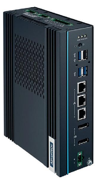
Advantech Australia Pty Ltd www.advantech.net.au
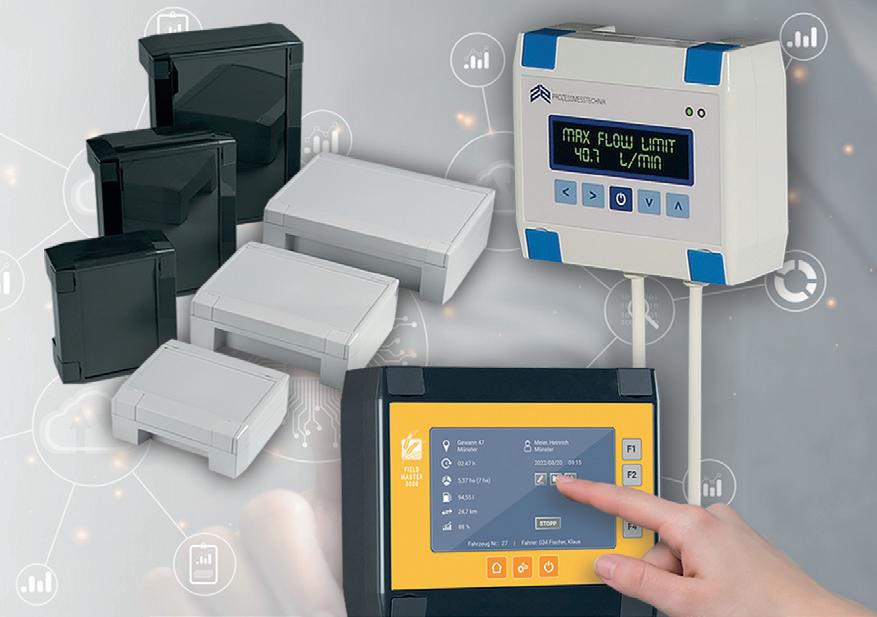
The OKW SOLID-BOX is designed for safeguarding sensitive touchscreens and control panels in harsh environments. Featuring IK08 impact protection and a high IP66/67 protection rating, the solid enclosure is suitable for a range of demanding environments. The OKW product range is made from flame-retardant PC+ABS-FR with improved heat resistance (Vicat/B 120 = 110°C). Additionally, the material is UL registered (94 V-0 from 1.5 mm) and has passed glow-wire testing (GWFI) at 960°C for 2.0 mm thickness. Available from stock in three sizes (135 x 115 x 50 mm, 180 x 145 x 60 mm, 225 x 175 x 70 mm) and two standard colours (light grey/RAL 7035 and anthracite grey/RAL 7016), the SOLIDBOX is versatile enough for a range of applications.
The SOLID-BOX offers plenty of space for components inside and also has a large, recessed control panel on the top. Pre-moulded mounts for VESA brackets (version 145 for VESA with 75 x 75 mm, version 175 for 100 x 100 mm) also enable simple wall mounting for the larger versions. With the optional housing feet (accessory), it can also be used as a table-top application with a secure stand.
The OKW housing also features contour-flush design panels to conceal the captive, rust-proof Torx screws. Additionally, recessed surfaces in the lower part enable the protected installation of interfaces, plugs and switches.
Whether used as an interface device, operating interface or HMI application, this robust enclosure fulfils all the demands of modern electronics packaging in industrial environments and protected outdoor areas.
ROLEC OKW Australia New Zealand P/L www.rolec-enclosures.com.au
ADLINK Technology Inc. has launched the AVA-7200 edge AI server and the AVA-1000 train to ground gateway. These solutions are designed to address the needs of the railway industry. From real-time obstacle detection to passenger information delivery, these systems are positioned to enhance safety, efficiency and passenger experience across all aspects of railway operations.
The AVA family of products, including the AVA-7200 and AVA-1000, covers a range of applications, including AI, 5G/Wi-Fi connectivity and onboard servers. The AVA-7200, powered by NVIDIA Ampere GPGPU and certified with EN50155 and EN45545, enables enhanced performance and immediate deployment readiness, thereby boosting safety and operational efficiency. Leveraging AI-powered video analysis, it also enables proactive risk mitigation and enhances overall railway safety.
The AVA-1000 features a fanless design, durability in extended temperature ranges and advanced TPM 2.0 technology, safeguarding data integrity and privacy. It also provides uninterrupted connectivity for train-to-ground communication. Furthermore, its compact and lightweight design simplifies installation, making it suitable for rail integrators operating in space-constrained environments.
ADLINK Technology Inc www.adlinktech.com
ICP Electronics Australia has launched the iEi PPC2-CW156A-ADLP, a fanless industrial panel PC designed for demanding environments, powered by Intel Alder Lake-P and Raptor Lake-P processors. It offers high performance and versatility, supporting 12th and 13th Gen Intel Core i7/i5/i3 mobile processors, with 8 GB of DDR4 SO-DIMM memory (expandable to 64 GB).
The 15.6 ″ full HD display features a 10-point capacitive touchscreen with anti-glare and anti-UV coating, to provide clear visibility in challenging light conditions. The fanless panel PC also supports 4K UHD output via HDMI, making it suitable for highresolution visual applications.

For connectivity, the panel PC is equipped with dual 2.5GbE LAN ports, four USB 3.2 Gen1 ports and multiple M.2 expansion slots, allowing for extensive peripheral integration. Remote management is enabled with optional IPMI 2.0 support, facilitating system monitoring and maintenance from afar.
Built with a durable aluminium and SECC enclosure, the PPC2-CW156A-ADLP is IP65-compliant, for protection against dust and water. Additionally, its fanless design allows for operation in harsh environments, withstanding temperatures ranging from -20 to 60°C, making it suitable for industrial applications.
ICP Electronics Australia www.icp-australia.com.au

The VECOW RCX-3750 PEG is an expandable GPU-accelerated system built to handle demanding AI, edge computing and industrial tasks. It is powered by Intel Core i9/i7/i5/i3 processors from the 14th generation (RPL-S Refresh/RPL-S/ADL-S), offering scalability and performance suited for AI inferencing and high-speed industrial applications.
The product supports up to seven PCIe slots, allowing for the integration of dual 900 W NVIDIA or AMD 2-slot full-length graphics cards. This gives the system a maximum power budget of 1800 W, making it suitable for AI workloads and inferencing processes that require significant GPU power. Its rich I/O includes two GigE LAN ports with TSN, four USB 3.2 Gen 2 ports, four COM ports and 32 isolated DIO, for a range of connectivity options.
The system also offers four SATA trays for 2.5 ″ SSD/HDD, two front-access M.2 SSD trays and three SIM card sockets for enhanced data storage and network capabilities. It operates in industrial environments with temperatures ranging from -25 to 45°C, and features flexible power input options ranging from 16–50 VDC and 90–220 VAC.
Designed for use in AI applications, 3D mapping, high-speed AOI and industrial edge computing, the RCX-3750 PEG delivers powerful performance in an expandable and configurable platform.
Backplane Systems Technology Pty Ltd www.backplane.com.au



Data is power. According to Dinesh Bharadia, an associate professor at UC San Diego in the Department of Electrical and Computer Engineering with an affiliate appointment in the Department of Computer Science and Engineering and the Qualcomm Institute (QI), “data will be the next decade’s ‘silicon’”.
The rapid growth of the Internet of Things means that data is more readily available and easily accessible than ever.
Sensors, ‘smart’ devices and software connect our world to the cloud, gathering information and enabling new types of data sharing and analysis. However, most of these tools are battery-powered and have difficulty sensing changes in real time.
Now, the tide is turning.
New research presented today and published in the Proceedings of the ACM Conference on Embedded Networked Sensor Systems from Bharadia and lead author Nagarjun Bhat, demonstrates that not only is passive sensing — or sensing without being connected to a power source — possible, it can be done at little cost without any specialised equipment.
A PhD student in electrical engineering, Bhat’s research focuses on ways to enable passive sensing using simple, widespread commodities.
His commodity of choice? Radio frequency identification tags, also known as RFID tags. Essentially, these small, flexible tags receive and transmit data from a chip to an RFID reader, which processes the information and sends it to a computer program for interpretation. They’re commonly embedded in products like clothing or library books for tracking inventory or in contactless transit fare payment cards.
Though they sound highly technical — and thus expensive — RFID tags run between a few cents to a few dollars per chip depending on the specs. And, with up to 90% of retailers using
RFID technology, the chips are widespread and easy to access.
To Bhat and Bharadia, who is also a faculty member of the UC San Diego Center for Wireless Communications, these chips appeared prime candidates for further experimentation.
“We wondered whether we could repurpose RFID tags to do battery-free sensing and tracking,” Bhat said. He explained that most current approaches to passive sensing rely on analog-digital converters, which measure stimuli, record them in raw data and convert them to digital values that are readable by computers.
But, these types of sensor interfaces are power-hungry; without additional batteries, they can last a matter of hours. Battery-based systems are also bulky, expensive and hard to scale sustainably.
“We were trying to see if we could use the chips to directly sense stimuli without needing converters,” he added. “We wanted to know if our environment could be automated in a way that was battery-free, able to sense parameters like temperature and humidity, and could connect to the Internet of Things to send raw data to a reader that could make sense of it all.”
Bhat and Bharadia aren’t the first ones to attempt making passive, wireless interfaces. Other researchers have pursued ultralow-power digital sensing that couples a sensor, converter and microprocessor into a single package. While an efficient design, these types of devices are expensive and bulky, and lack the ability to sense and report stimuli in real time. They only send data to a reader when it’s requested and need complex electronic circuitry for their interface.

“If I wanted to use digital sensing for a biomedical application like monitoring a patient’s heart rate, I might not be able to access that data for 10 minutes,” Bhat said. “That’s a problem.”
Analog sensing — the category in which Bhat and Bharadia’s sensors fall — directly perceives environmental stimuli. Unlike digital interfaces, analog ones convert the change in voltage/current produced by sensors into parameters of a wireless signal.
Bhat noted that although “there has been good work done so far” on passive analog systems, most of the research has relied on customised sensors that are purpose-built and only suited for a particular application. These systems are difficult to generalise, he explained, adding that “you’d have to redesign all sensors on the market to make them commercially available”.
That’s why he chose RFID tags as the workhorse of his passive sensors: they’re commercialised, cheap and require little custom hardware to be deployed or read.
“We took the concept of analog sensing and made it real-time,” Bhat said. “You don’t need any fancy interfaces, specialised readers or batteries to access the data — all you need are some commercially available RFID tags, antennas and readers.”
Bhat’s battery-free RFID sensors enable new use cases like improved agricultural management, real-time athletic performance metrics and occupancy detection.
Currently, automatic irrigation systems generally rely on a smaller quantity of bigger sensors that cover large areas. This can be cost-
effective, although it comes at the expense of data specificity. RFIDbased passive trackers can do both. By deploying soil moisture sensors at scale around a field, it’s possible to use a few RFID readers to remotely measure moisture content at a much more granular level and adjust how water is distributed based on current conditions.
This type of immediate data can also be valuable for athletes. For instance, many UC San Diego athletes engage in force plate testing as part of their training, where they jump on force plates that measure their strength, power and posture. These tests must be done at a special facility and can be expensive. Bhat’s paper describes how RFID sensor tags could be used to bring these tests “in-house” by embedding them in shoe soles to measure an athlete’s jumping force.
Or, RFID tags can be placed in parking garages to measure occupancy and map where and how many spaces are being used. A chip could be added to the floor of every space; when a car pulls into the spot and covers the light-sensitive sensor, the tag recognises that the spot is occupied and can send that information to a central location.
At the end of the day, however, Bharadia and Bhat see bigger uses for their work.
“AI is everywhere now,” Bharadia said, adding that AI is powered by data enabled by sensors. “We’re at the cusp of a revolution where new sensors will be collecting the data that will power the next generation of AI. Using battery-less sensors lets us collect a lot of information that’s otherwise challenging to access — they can empower data collection, and this innovation marks a really important direction for the future.”
congatec has launched the COM Express Compact Computer-on-Modules with AMD Ryzen Embedded 8000 Series processors. The modules are based on the computing cores of the Ryzen processors featuring up to eight ‘Zen 4’ cores, innovative XDNA NPU and Radeon RDNA 3 graphics.
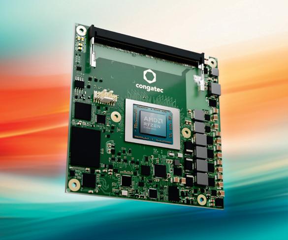
This makes the conga-TCR8 Type 6 modules suitable for high-volume applications requiring a combination of advanced AI, graphics and computing power. OEMs in medical imaging, test & measurement, AI-supported POS/POI systems and professional gaming can also leverage these long-term available COM Express Compact modules to accelerate innovation. With a broad, scalable TDP range of 15–54 W, these modules are also suitable for upgrading existing designs.
The conga-TCR8 computer-on-modules support up to 128 GB DDR5-5600 memory with error correction code (ECC) for dataintensive and data-critical applications. With the integrated AMD XDNA NPU (16 TOPS) and AMD Radeon RDNA 3 graphics, the modules deliver a combined computing power of up to 39 TOPS. They also support immersive graphics output on up to four displays with resolutions as high as 8K. For fast peripheral connectivity, they offer six PCIe Gen 4 (8 lanes) with PEG x8 Gen 4, three DisplayPort (DP) interfaces, one eDP or LVDS, four USB 3.2 Gen 2 ports, and four USB 2.0 ports.
The modules are also available as application-ready aReady. COMs, with custom pre-installed and validated operating systems like ctrlX OS, Ubuntu and/or RT Linux, optional system consolidation via aReady.VT, and IoT connectivity via aReady.IOT. On request, the modules can be pre-installed with the customer’s application, allowing for simple plug-and-play integration into the finished system.
Congatec Australia Pty Ltd www.congatec.com




Emerson has launched its new Energy Manager solution, a pre-engineered hardware and software offering designed to simplify industrial electricity monitoring with quick setup and intuitive operation. Ready out of the box, the Energy Manager solution monitors asset energy use in real time, allowing manufacturers to gain deeper insight into energy consumption and operating costs, lowering carbon dioxide (CO2) emissions and enhancing energy and operational efficiency.
The Energy Manager solution provides energy measurements in real time, allowing plant managers to quickly view detailed values and see savings opportunities, such as idle consumption and peak loads. The software’s easy-to-use dashboard provides asset-specific energy use, associated costs and CO2 emissions for up to 10 end points (expandable to 50 endpoints with a licence).
This level of visibility gives organisations greater control to identify idle machines and enhance machine schedules during off-peak hours, reducing electricity use across the plant floor and lowering overall utility costs.
Highly scalable and easy to integrate with new or existing energy meters, the Energy Manager solution is also easy to commission. The software is available either pre-installed on edge hardware, such as the PACSystems RXi2-BP industrial PC, or as a standalone application that can be installed in a virtualised environment.
The Energy Manager solution gives operators, facility managers and corporate sustainability teams greater visibility and deeper understanding of energy consumption at all times. This can better position companies to track and reach targets, comply with regulations and reduce environmental impact.
For more extensive media and utilities monitoring, the Energy Manager can be paired with the Emerson Compressed Air Manager to provide a streamlined view of energy costs and compressed air usage of machines across a production line, factory and site.
Emerson www.emerson.com/au/automation


The Quectel EG91-EX LTE Cat 1 module, launched by Quectel Wireless Solutions, has received the EU Type Examination Certificate for RED Cybersecurity.
The LTE Cat 1 module is optimised for M2M and IoT applications. Utilising 3GPP Rel-11 LTE technology, it offers data rates of up to 10 Mbps for downlink and 5 Mbps for uplink. These capabilities make the EG91 series suitable for IoT applications that prioritise longevity and reliability over high-speed connectivity, facilitating performance on the LTE network.
The Radio Equipment Directive 2014/53/EU (RED) establishes a regulatory framework for placing radio equipment on the market and sets requirements for safety and health, electromagnetic compatibility and the efficient use of the radio spectrum.
Devices covered by RED DA include equipment that uses radio technology for communication over the internet such as mobile phones, tablets, electronic cameras, telecommunication equipment, IoT devices that can transmit data over the internet, toys and childcare equipment such as baby monitors, wearable devices such as smartwatches and fitness trackers, and connected industrial devices.
Quectel
www.quectel.com
ICP Electronics Australia has launched the ICP DAS tET-DA2, a compact and versatile PoE Ethernet module featuring 2-channel isolated analog outputs, designed to meet the needs of various industrial applications. This module allows for programmable output ranges across all analog outputs, supporting 0–10 V, 0–20 mA and 4–20 mA, making it adaptable for a range of tasks.
The module features robust protection mechanisms, including 4 kV ESD protection and 3000 VDC intra-module isolation for enhanced safety in demanding industrial environments. The builtin web server facilitates easy configuration and monitoring, while support for Modbus TCP/UDP, MQTT and SNMP V2c protocols enhances its integration capabilities within diverse systems.
Additionally, the tET-DA2 is equipped with a dual watchdog timer to facilitate continuous operation. Its I/O pair connection feature (push and pull) enables communication between modules, further expanding its application potential.
Suitable for use in industrial automation, industrial machinery, building automation, food and beverage systems, semiconductor fabrication and control systems, the tET-DA2 tiny Ethernet module is designed to enhance analog output control. Its compact size and PoE capability make it a practical and efficient solution for modern industrial environments.
ICP Electronics Australia www.icp-australia.com.au

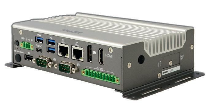
Backplane Systems Technology has launched the iBase AGS104T, the latest addition to IBASE’s IoT gateway line-up, powered by Intel Atom x7433RE and x7211RE processors (formerly known as Amston Lake). Designed for demanding industrial environments, this fanless gateway computer features an extended operating temperature range of -40 to 70°C, making it suitable for critical IoT deployments. The AGS104T supports up to 16 GB of DDR5-4800 memory, thereby enabling high-speed data processing. It features dual 2.5G Ethernet ports, versatile COM ports (RS232/422/485) and expansion options through M.2 and Mini PCI-E slots. For added security, it comes equipped with TPM 2.0, a wide-range 9~36 VDC power input with comprehensive voltage protections and GPIO 4-in/4-out for enhanced control functions.
Compact and flexible, the edge computing system supports both DIN-rail and wall-mount installations, offering a range of I/O interfaces, including HDMI, DisplayPort and USB 3.2. These features make it suitable for various industrial applications. Backplane Systems Technology Pty Ltd www.backplane.com.au
Amanda Morris, Northwestern University

Step aside hard, rigid materials. There is a new soft, sustainable electroactive material in town — and it’s poised to open new possibilities for medical devices, wearable technology and human–computer interfaces.
UNorthwestern University materials scientists have developed materials made of tiny, flexible nano-sized ribbons that can be charged just like a battery to store energy or record digital information. Highly energy efficient, biocompatible and made from sustainable materials, the systems could give rise to new types of ultralight electronic devices while reducing the environmental impact of electronic manufacturing and disposal.
The study was published in the journal Nature
With further development, the new soft materials could be used in low-power, energy-efficient microscopic memory chips,
like medical implants. In today’s wearable devices, electronics are clunkily strapped to the body with a wristband. But, with the new materials, the wristband itself could have electronic activity.
“This is a wholly new concept in materials science and soft materials research,” said Northwestern’s Samuel I. Stupp, who led the study. “We imagine a future where you could wear a shirt with air conditioning built into it or rely on soft bioactive implants that feel like tissues and are activated wirelessly to improve heart or brain function.
plications with classic electroactive materials. It’s not practical to put hard materials into our organs or in shirts that people can wear. We need to bring electrical signals into the world of soft materials. That is exactly what we have done in this study.”
Stupp is the Board of Trustees Professor of Materials Science and Engineering, Chemistry, Medicine and Biomedical Engineering at Northwestern. He also has served over the past decade as director of the U.S. Department of Energy-supported Center for Bio-Inspired Energy Science, where this research began. Stupp has appointments in the McCormick

School of Engineering, Weinberg College of Arts and Sciences and Northwestern University Feinberg School of Medicine. Yang Yang, a research associate in Stupp’s laboratory, is the paper’s first author.
The secret behind the new material is peptide amphiphiles, a versatile platform of molecules previously developed in Stupp’s laboratory. These self-assembling structures form filaments in water and have already demonstrated promise in regenerative medicine. The molecules contain peptides and a lipid segment, which drives the molecular self-assembly when placed in water.
In the new study, the team replaced the lipid tail with a miniature molecular segment of a plastic called polyvinylidene fluoride (PVDF). But they kept the peptide segment, which contains sequences of amino acids. Commonly used in audio and sonar technologies, PVDF is a plastic with unusual electrical properties. It can generate electrical signals when pressed or squeezed — a property known as piezoelectricity. It also is a ferroelectric material, which means it has a polar structure that can switch orientation by 180 degrees using an external voltage.
The dominant ferroelectrics in technology are hard materials and often include rare or toxic metals, such as lead and niobium.
“PVDF was discovered in the late 1960s and is the first known plastic with ferroelectric properties,” Stupp said. “It has all the robustness of plastic while being useful for electrical devices. That makes it a very
high-value material for advanced technologies. However, in pure form, its ferroelectric character is not stable, and, if heated above the so-called Curie temperature, it loses its polarity irreversibly.”
All plastics, including PVDF, contain polymers, which are giant molecules typically composed of thousands of chemical structural units. In the new study, the Stupp laboratory precisely synthesised miniature polymers with only three to seven vinylidene fluoride units. Interestingly, the miniature segments with four, five or six units are programmed by nature’s beta-sheet structures, which are present in proteins, to organise into a stable ferroelectric phase.
“It was not a trivial task,” Stupp said. “The combination of two unlikely partners — peptides and plastics — led to a breakthrough in many respects.”
Not only were the new materials equally ferroelectric and piezoelectric as PVDF, but the electroactive forms were stable, with the ability to switch polarity using extremely low external voltages. This opens the door for low-power electronics and sustainable nanoscale devices. The scientists also envision developing new biomedical technologies by attaching bioactive signals to the peptide segments, a strategy already used in Stupp’s regenerative medicine research. This offers the unique combination of electrically active materials that are also bioactive.
To create the sustainable structures, Stupp’s team simply added water to trigger the selfassembly process. After dunking the materials,
Stupp was amazed to find that they achieved the highly sought-after ferroelectric properties of PVDF.
In the presence of an external electric field, ferroelectric materials flip their polar orientation — similar to how a magnet can be flipped from north to south and back again. This property is a key ingredient for devices that store information, an important feature for artificial intelligence technologies. Surprisingly, the investigators found that “mutations” in the peptide sequence could tune properties related to ferroelectricity or even transform the structures into materials that are ideal for actuation or energy storage known as “relaxor phases”.
“Peptide sequence mutations in biology are the source of pathologies or biological advantages,” Stupp said. “In the new materials, we mutate peptides to tune their properties for the physical world.
“Using nanoscale electrodes, we could potentially expose an astronomical number of self-assembling structures to electric fields. We could flip their polarity with a low voltage, so one serves as a ‘one’ and the opposite orientation serves as a ‘zero’. This forms binary code for information storage. Adding to their versatility, and in great contrast to common ferroelectrics, the new materials are ‘multiaxial’ — meaning they can generate polarity in multiple directions around a circle rather than one or two specific directions.”
To flip their polarity, even soft ferroelectric materials like PVDF or other polymers typically require a substantial external electric field. The new structures, however, require incredibly low voltage.
“The energy required to flip their poles is the lowest ever reported for multiaxial soft ferroelectrics,” Stupp said. “You can imagine how much energy this will save in increasingly energy-hungry times.”
The new materials also have innate environmental benefits. Unlike typical plastics, which linger in the environment for centuries, the Stupp laboratory’s materials could be biodegraded or reused without the use of harmful, toxic solvents or highenergy processes.
“We are now considering the use of the new structures in non-conventional applications for ferroelectrics, which include biomedical devices and implants as well as catalytic processes important in renewable energy,” Stupp said. “Given the use of peptides in the new materials, they lend themselves to functionalisation with biological signals. We are very excited about these new directions.”
STMicroelectronics has launched the PWD5T60 three-phase driver with a ready-to-use evaluation board that supports flexible control strategies. Suitable for applications up to 500 V, the PWD5T60 integrates a gate driver and six power MOSFETs with RDS(ON) of 1.38Ω, enabling the device to achieve an enhanced energy to area rating. Zero-drop bootstrap diodes are also built-in, requiring minimal external components to complete the circuit in only 30% of the board area of an equivalent driver built with discrete components. The propagation delays of high-side and low-side MOSFETs are closely matched, which eliminates cycle distortion and increases flexibility to set the operating frequency for optimum response and energy efficiency.
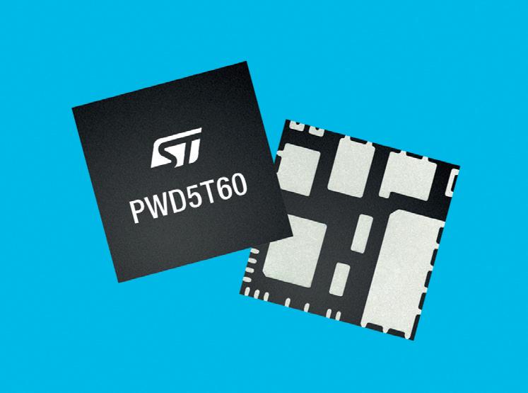
The EVLPWD-FAN-PUMP evaluation board, released at the same time, helps developers explore the value this driver can deliver in projects up to 100 W. The board combines the PWD5T60 with an STM32G0 microcontroller (MCU) that can handle field-oriented control (FOC) or 6-step control of permanent magnet synchronous motors (PMSMs) and brushless DC (BLDC) motors. With configurable single or three-shunt sensing and leveraging the PWD5T60’s high feature integration to achieve a compact, circular form factor, the board is optimised for use with fans and pumps. The board also features a power-supply stage to generate 12 V and 3.3 V supply voltages for the application and comes with a complete AC line filter at the input.
The PWD5T60 has a smart shutdown feature that uses a comparator for fast-acting overcurrent prevention. The output turns off immediately when a fault is detected, while the subsequent output-disable duration is programmed by connecting a capacitor and optional pull-up resistor to a dedicated pin. The turnoff response is unaffected by these components, letting product developers optimise the duration to allow time for faults to clear while enabling instant turn-off.
The driver has a wide input supply voltage range from 9–20 V for optimum flexibility, while CMOS/TTL-compatible logic inputs down to 3.3 V simplify interfacing with a host controller.
The PWD5T60 is in full production and available in a compact 12 x 12 mm VFQFPN package only 0.95 mm high.
STMicroelectronics Pty Ltd www.st.com
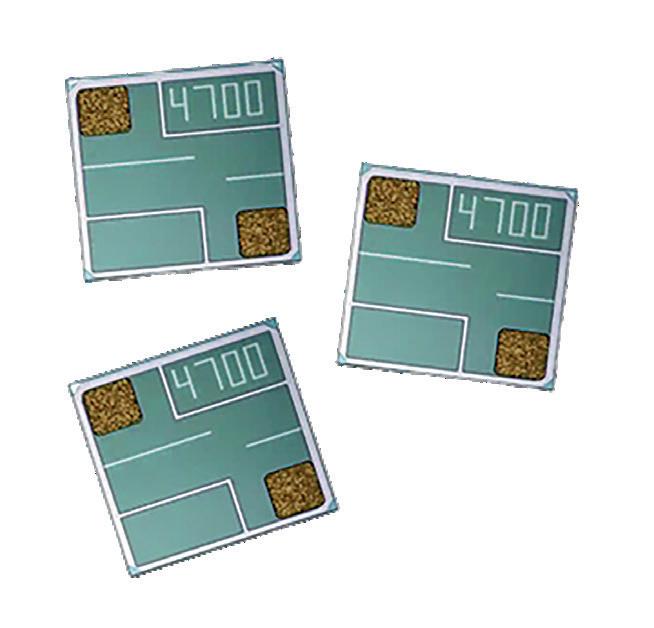
KYOCERA AVX’s WBR Series of topcontact, bottom-isolated microwave chip resistors are ruggedly constructed, rated for up to 250 mW DC power and built in an 0202 chip outline. They are designed to deliver ultra-stable performance in a range of applications that require thermos compression, epoxy or ultrasonic attachment.
The resistors are suitable for hybrid circuits and are versatile for other applications, including medical implantable devices, multichip modules (MCM), test and measurement instrumentation, high-reliability microelectronics, and aerospace and defence.
Additional features include: frequency range up to 10 GHz; resistance from 7.5 Ω to 12M Ω; tolerance of 1%; and 100% laser trimming for tight tolerances. Richardson RFPD www.richardsonrfpd.com
Backplane Systems Technology has launched the VECOW EAC-5100OOB, an embedded AI computing system designed for advanced edge AI applications, powered by NVIDIA Jetson AGX Orin technology. Delivering up to 275 TOPS of AI performance, it features the latest NVIDIA Ampere architecture with 2048 CUDA cores and 64 Tensor cores, providing a performance boost for real-time AI processing. This system supports a range of power inputs from 9–50 V, making it suitable for industrial, automotive and mobile applications.
The computing system offers extensive connectivity, including six GigE LAN ports, four with PoE+ support, five USB 3.1 ports and one digital display supporting 4K60 resolution. For flexible integration, it features a PCIe Gen 3 x8 slot, isolated CANbus, RS-232/422/485 ports and support for automotive cameras via FAKRA-Z connectors. Its rugged design enables performance in harsh environments, operating in temperatures from -25 to 70°C and meeting military-grade standards for shock and vibration resistance.
With built-in out-of-band (OOB) management, the EAC-5100-OOB facilitates remote disaster recovery, allowing operators to manage and reboot devices even during system failures. This makes it a versatile solution for edge AI deployments.
Backplane Systems
Technology Pty Ltd www.backplane.com.au


The future of wireless technology — from charging devices to boosting communication signals — relies on the antennas that transmit electromagnetic waves becoming increasingly versatile, durable and easy to manufacture.
Researchers at Drexel University and the University of British Columbia believe kirigami, the ancient Japanese art of cutting and folding paper to create intricate three-dimensional designs, could provide a model for manufacturing the next generation of antennas.
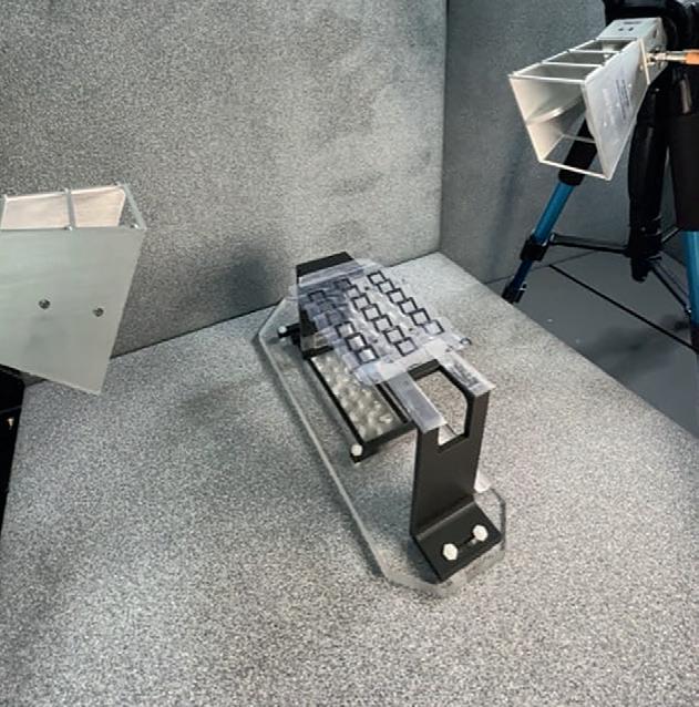
Recently published in the journal Nature Communications , research from the Drexel-UBC team showed how kirigami — a variation of origami — can transform a single sheet of acetate coated with conductive MXene ink into a flexible 3D microwave antenna whose transmission frequency can be adjusted simply by pulling or squeezing to slightly shift its shape.
The proof of concept is significant, according to the researchers, because it represents a new way to quickly and cost-effectively manufacture an antenna by simply coating aqueous MXene ink onto a clear elastic polymer substrate material.
“For wireless technology to support advancements in fields like soft robotics and aerospace, antennas need to be designed for tuneable performance and with ease of fabrication,” said Yury Gogotsi, PhD, Distinguished University and Bach Professor in Drexel’s College of Engineering, and a co-author of the research. “Kirigami is a natural model for a manufacturing process, due to the simplicity with which complex 3D forms can be created from a single 2D piece of material.”
Standard microwave antennas can be reconfigured either electronically or by altering their physical shape. However, adding the neces-
sary circuitry to control an antenna electronically can increase its complexity, making the antenna bulkier, more vulnerable to malfunction and more expensive to manufacture.
By contrast, the process demonstrated in this joint work leverages physical shape change and can create antennas in a variety of intricate shapes and forms. These antennas are flexible, lightweight and durable, which are crucial factors for their survivability on movable robotics and aerospace components.
To create the test antennas, the researchers first coated a sheet of acetate with a special conductive ink, composed of a titanium carbide MXene, to create frequency-selective patterns. MXene ink is particularly useful in this application because its chemical composition allows it to adhere strongly to the substrate for a durable antenna and can be adjusted to reconfigure the transmission specifications of the antenna.
MXenes are a family of two-dimensional nanomaterials discovered by Drexel researchers in 2011 whose physical and electrochemical properties can be adjusted by slightly altering their chemical composition. MXenes have been widely used in the last decade for applications that require materials with precise physiochemical behaviour, such as electromagnetic shielding, biofiltration and energy storage. They have
also been explored for telecommunications applications for many years due to their efficiency in transmitting radio waves and their ability to be adjusted to selectively block and allow transmission of electromagnetic waves.
Using kirigami techniques, originally developed in Japan the 4th and 5th centuries A.D., the researchers made a series of parallel cuts in the MXene-coated surface. Pulling at the edges of the sheet triggered an array of square-shaped resonator antennas to spring from its two-dimensional surface. Varying the tension caused the angle of the array to shift — a capability that could be deployed to quickly adjust the communications configuration of the antennas.
The researchers assembled two kirigami antenna arrays for testing. They also created a prototype of a co-planar resonator — a component used in sensors that naturally produces waves of a certain frequency — to showcase the versatility of the approach. In addition to communication applications, resonators and reconfigurable antennas could also be used for strain-sensing, according to the team.
“Frequency selective surfaces, like these antennas, are periodic structures that selectively transmit, reflect, or absorb electromagnetic waves at specific frequencies,” said Mohammad Zarifi, principal research chair, an associate professor at UBC, who helped lead the research. “They have active and/or passive structures and are commonly used in applications such as antennas, radomes, and reflectors to control wave propagation direction in wireless communication at 5G and beyond platforms.”
The kirigami antennas proved effective at transmitting signals in three commonly used microwave frequency bands: 2-4 GHz,
THESE FINDINGS ARE THE FIRST STEP TOWARD INTEGRATING THE COMPONENTS ON RELEVANT STRUCTURES AND WIRELESS DEVICES.
4-8 GHz and 8-12 GHz. Additionally, the team found that shifting the geometry and direction of the substrate could redirect the waves from each resonator.
The frequency produced by the resonator shifted by 400 MHz as its shape was deformed under strain conditions — demonstrating that it could perform effectively as a strain sensor for monitoring the condition of infrastructure and buildings.
According to the team, these findings are the first step toward integrating the components on relevant structures and wireless devices. With kirigami’s myriad forms as their inspiration, the team will now seek to optimise the performance of the antennas by exploring new shapes, substrates and movements.
“Our goal here was to simultaneously improve the adjustability of antenna performance as well as create a simple manufacturing process for new microwave components by incorporating a versatile MXene nanomaterial with kirigami-inspired designs,” said Omid Niksan, PhD, from University of British Columbia, who was an author of the paper. “The next phase of this research will explore new materials and geometries for the antennas.”

ADLINK Technology Inc. has launched the SBC35 Series of 3.5 ″ Single Board Computers (SBC). This series introduces a range of motherboards engineered to enhance efficiency in compact spaces. The SBC35 Series features two models: the SBC35-RPL, powered by the 13th Gen Intel Core processors, and the SBC35-ALN, equipped with the Intel N97 processor. The series also features a range of I/O modules and SBC-FM Adaptive Function Modules (AFM) that enhance system capabilities. These advancements make the SBC35 Series suitable for a range of applications in automation, transportation, medical fields and smart city projects.
The single board computers showcase two models in a 146 x 102 mm, 3.5 ″ SBC form factor, each designed to maximise space and functionality in demanding settings. While the SBC35-RPL supports up to 64GB DDR5 4800MHz RAM and four independent displays, the SBC35-ALN accommodates up to 16GB DDR5 4800MHz RAM and three independent displays. Both units are equipped with a range of connectivity options, including four USB ports and versatile M.2 slots (2280 M Key, 2230 E Key, 3042 B Key), supplemented by dual RS-232/422/485, and additional dual RS-232 ports, audio, and digital I/O capabilities. Optional TPM 2.0 further enhances security, making these models adaptable for a range of industrial applications.
The single board computers also feature SBC-FM Adaptive Function Modules, which offer flexible I/O expansion and customerdriven customisation. These modules are designed for the SBC35 series and include reserved connectors such as PCIe, USB and LPC/eSPI, enabling customisation and functionality for diverse applications. They are also designed to integrate with the mainboard, either vertically or in parallel, through an FPC cable. This provides high thermal resilience under extreme conditions. ADLINK Technology Inc www.adlinktech.com
In a leap toward more powerful and efficient computer chips, researchers at the University of Virginia have confirmed a key principle governing heat flow in thin metal films — a critical component in the race to design faster, smaller and more efficient devices.
University of Virginia School of Engineering and Applied Science
This work, published in Nature Communications and supported by the Semiconductor Research Corporation in collaboration with Intel, offers a breakthrough in understanding how thermal conductivity works in metals used within next-generation chips, unlocking possibilities for advancements in technology at scales once thought unattainable.
“As devices continue to shrink, the importance of managing heat becomes paramount,” said lead researcher and mechanical and aerospace engineering PhD student Md Rafiqul Islam. “Consider high-end gaming consoles or AI-driven data centres, where constant, high-power processing often leads to thermal bottlenecks. Our findings provide a blueprint to mitigate these issues by refining the way heat flows through ultra-thin metals like copper.”
Copper, widely used for its excellent conductive properties, faces significant challenges as devices scale down to nanometre dimensions. At such small scales, even the best materials experience a drop in performance due to increased heat — a phenomenon that’s amplified in copper, leading to lower conductivity and efficiency. To address this, the UVA team focused on a crucial element of thermal science known as Matthiessen’s rule, which they validated in ultra-thin copper films. The rule, which traditionally helps predict how different scattering processes influence electron flow, had never been thoroughly confirmed in nanoscale materials until now.
Using a novel method known as steadystate thermoreflectance (SSTR), the team measured copper’s thermal conductivity and cross-checked it with electrical resistivity data. This direct comparison demonstrated that Matthiessen’s rule, when applied with specific parameters, reliably describes the way heat moves through copper films even at nanoscale thicknesses.

Why does this matter? In the world of verylarge-scale integration (VLSI) technology, where circuits are packed into incredibly tight spaces, effective heat management directly translates to improved performance. This research not only points to a future where our devices run cooler but also promises a reduction in the amount of energy lost to heat — a pressing concern for sustainable technology. By confirming that Matthiessen’s rule holds even at nanoscale dimensions, the team has paved the way for refining materials that interconnect circuits in advanced computer chips, setting a standard for material behaviour that manufacturers can rely on.
“Think of it as a roadmap,” said Patrick E. Hopkins, Islam’s adviser and the Whitney Stone Professor of Engineering. “With the validation of this rule, chip designers now have a trusted guide to predict and control how heat will behave in tiny copper films. This is a game changer for making chips that meet the energy and performance demands of future technologies.”
The success of this study represents a collaboration between UVA, Intel and the Semiconductor Research Corporation, highlighting the strength of academic–industry partnerships. The findings promise significant applications in the development of next-generation CMOS technology — the backbone of modern electronics. CMOS, or complementary metal-oxide-semiconductor, is the standard technology for building integrated circuits that run everything from computers and phones to automotive and medical devices.
By combining experimental insights with advanced modelling, UVA researchers have opened a door to materials that not only drive more efficient devices but also hold the potential for impactful energy savings across the industry. In a field where every degree of temperature control counts, these insights mark a vital step forward for the electronics industry, making a future of cooler, faster and more sustainable devices more achievable than ever.
David Nutt, Cornell University

Gallium nitride-based semiconductors have been a boon for high-frequency and power electronics. They’ve also revolutionised energy-efficient LED lighting. But no semiconductor wafer has been able to do both at the same time efficiently.
Now Cornell researchers, in collaboration with a team at the Polish Academy of Sciences, have developed the first dual-sided — or “dualtronic” — chip that combines its photonic and electronic functions simultaneously, an innovation that could shrink the size of functional devices, make them more energy efficient and reduce manufacturing costs.
The team’s paper, ‘Using Both Faces of Polar Semiconductor Wafers for Functional Devices’, was published on 25 September in Nature . The co-lead authors are doctoral students Len van Deurzen and Eungkyun Kim.
The project was led by Debdeep Jena, the David E. Burr Professor of Engineering in the School of Electrical and Computer Engineering and Department of Materials Science and Engineering, and Huili Grace Xing, the William L. Quackenbush Professor of Electrical and Computer Engineering and of Materials Science and Engineering, both in Cornell Engineering.
Gallium nitride (GaN) is unique among wide-bandgap semiconductors because it has a large electronic polarisation along its crystal axis, which gives each of its surfaces dramatically different physical and chemical properties. The gallium, or cation, side has proved useful for photonic devices such as LEDs and lasers, while the nitrogen, or anion, side can host transistors.
The Jena-Xing Laboratory set out to make a functional device in which a high electron mobility transistor (HEMT) on one side drives light-emitting diodes (LEDs) on the other — a feat that hasn’t been achieved in any material.
“To our knowledge, nobody has made active devices on both sides, not even for silicon,” van Deurzen said. “One of the reasons is that there’s no additional functionality you get from using both sides of a silicon wafer because it’s cubic; both sides are basically the same. But gallium nitride is a polar crystal, so one side has different physical and chemical properties than the other, which gives us an extra degree in designing devices.”
The project was initially conceived at Cornell by Jena and former postdoctoral researcher Henryk Turski, a co-senior author of the paper, along with Jena and Xing. Turski worked with a team at the Polish Academy of Sciences’ Institute of High Pressure Physics to grow transparent GaN substrates on a single crystal wafer roughly 400 microns thick. The HEMT and LED heterostructures were then grown in Poland by molecular beam epitaxy. After the epitaxy was completed, the chip was shipped to Cornell, where Kim built and processed the HEMT on the nitrogen polar face.
“The nitrogen polar side is more chemically reactive, which means during device processing the electron channel can be damaged quite easily,” Kim said. “A challenge with nitrogen polar transistor fabrication is to make sure all the plasma processes and the chemical treatment do not damage the transistors. So there was a lot of process development that had to be done for fabricating and designing that transistor.”
Next, van Deurzen built the LED on the metal polar face, using a thick positive photo resist coating to protect the previously processed n-polar face. After each stage, the researchers measured their respective device characteristics and found they had not changed.
“It’s actually a very feasible process,” van Deurzen said. “The devices do not degrade. And this is obviously important if you want to use this as a real technology.”
Since no one has made a double-sided semiconductor device before, the team had to invent a new method to test and measure it. They assembled a “crude” double-side-coated glass plate and wire-bonded one side of the wafer to it, which allowed them to probe both sides from the top. Because the GaN substrates were transparent for the entire visible range, the light was able to transmit through. The single HEMT device succeeded in driving a large LED, turning it on and off at kilohertz frequencies — plenty for a working LED display.
Currently, LED displays have a separate transistor and independent fabrication processes. An immediate application for the dualtronic chip is microLEDs: fewer components, occupying a smaller footprint and requiring less energy and materials, and manufactured more quickly at a lower cost.
“A good analogy is the iPhone,” Jena said. “It is, of course, a phone, but it is so many other things. It’s a calculator, it’s a map, it lets you check the internet. So there’s a bit of a convergence aspect of it. I would say our first demonstration of ‘dualtronics’ in this paper is convergence of maybe two or three functionalities, but really it’s bigger than that. Now you may not require the different processors to perform different functions, and reduce the energy and speed lost in the interconnections between them that requires further electronics and logic. Many of those functionalities shrink into one wafer with this demonstration.”
Other applications include complementary metal-oxide-semiconductor (CMOS) devices with a polarisation-induced n-channel transistor (which uses electrons) on one side and a p-channel transistor (containing holes) on the other.
In addition, because the GaN substrates have a high piezoelectric coefficient, they can be used as bulk acoustic wave resonators for filtering and amplifying radio frequency signals in 5G and 6G communications. The semiconductors could also incorporate lasers instead of LEDs for “LiFi” — ie, light-based — transmissions.
“You could essentially extend this to enable the convergence of photonic, electronic and acoustic devices,” van Deurzen said. “You’re essentially limited by your imagination in terms of what you could do, and unexplored functionalities can emerge when we try them in the future.”
Yamaha Robotics Europe has launched the YRi-V HS optical inspection (AOI) system, featuring faster performance, high-resolution imaging and improved accuracy for inspecting surface-mounted LEDs.
The YRi-V HS configuration is for electronic manufacturers in all market sectors, from consumer to industrial and automotive, seeking greater inspection resolution with high production throughput. As circuit designers increasingly adopt components with tiny feature sizes, to deliver extra functionality and comply with tough constraints on the overall form factor, manufacturers need inspection systems with greater resolution to enable proper quality control. On the other hand, maintaining high throughput is necessary to fulfil productivity targets.
The YRi-V HS combines high inspection resolution and high throughput to handle components such as SMD chips and IC packages with fine-pitch I/Os and BGAs with a high I/O count. With its enlarged, square field of view (FOV) and 25 MP camera, the YRi-V HS can image a complete assembly or selected area up to 1.6 times faster than ordinary high-resolution systems.
The optical inspection system also integrates an advanced laser system for height measurement and coplanarity checking of components, such as LEDs in lighting products, overcoming the limitations cameras face in detecting component height. Laser profiling overcomes the imaging challenges presented by the LEDs’ transparent or opaque lenses, offering effective quality control for manufacturers to address LED lighting opportunities in automotive, consumer and industrial markets. Laser profiling enhances accurate imaging of components with highly reflective surfaces, like wafer-level chip-scale packages, which helps improve end-of-line yield and reduce rework.
Hawker Richardson is the exclusive supplier of Yamaha SMT line products in Australasia, providing regional access to Yamaha’s advanced inspection solutions.
Hawker Richardson www.hawkerrichardson.com.au
University of Sydney

A team of researchers has for the first time successfully used lasers to generate guided sound waves on the surface of a microchip. These acoustic waves, akin to the surface waves produced during an earthquake, travel across the chip at frequencies nearly a billion times higher than those found in Earth tremors.
By containing the sound wave on the surface of a chip, it can more easily interact with the environment, making it a perfect candidate for advanced sensing technologies.
The findings have been published in the APL Photonics journal of the American Institute of Physics.
“The use of sound waves on the surface of a microchip has application in sensing, signal processing and advanced communications technology,” said senior author and project lead Dr Moritz Merklein from the University of Sydney Nano Institute and School of Physics. “We can now start to think about new designs for chips that use light and sound instead of electricity.
Lead author Govert Neijts, a student from the University of Twente in the Netherlands who spent nine months at the University of Sydney labs, said: “Typically, surface acoustic waves are ‘excited’ using electronics. Here we use photonics, or light energy, to produce the sound wave. This approach has multiple advantages, chief of which is that light does not produce the heat in the chip that electronic excitation causes.”
Using special glass made from germanium, arsenic and selenide known as GeAsSe, the scientists were able to achieve remarkable results, including measurements indicating strong interactions between light and sound.
This innovative research demonstrates how lasers can be used to create and detect high-frequency surface acoustic waves using novel materials as a ‘wave guide’.
“The material is considered a soft glass. This means that unlike many materials, it operates as a guide for the high-frequency sound waves and lets them more freely interact with the light waves we put into the chip,” Merklein said.
The ability to generate and manipulate these high-frequency acoustic waves opens
a world of possibilities for new applications in sensing and signal processing.
Co-author Dr Choon-Kong Lai, a postdoctoral researcher in the Institute of Photonics and Optical Science at the University of Sydney, said: “Imagine sensors that can detect minute changes in the environment or advanced signal processing techniques that enhance communication technologies. Our innovative approach not only paves the way for more sensitive and efficient devices but also expands the potential for integrating acoustic and optical technologies on a single chip.”
The team previously demonstrated ‘capturing’ light information inside phononics, or sound waves within a chip. This ‘lightning inside thunder’ innovation was a world first at the time.
“We have developed this work to be able to manage and guide high-frequency sound wave information on the surface of a chip. This is an important contribution for the development of emergent sensing technologies,” said coauthor and research team leader, Professor Ben Eggleton, Pro-Vice-Chancellor (Research) at the University of Sydney.
The technique used by the researchers is known as stimulated Brillouin scattering (SBS). This is created by an enhanced feedback loop between photons (light) and phonons (sound).
As light moves around the chip or an optical fibre, it creates sound vibrations. Previously seen as a nuisance in optical communication, scientists then realised they could couple and enhance this vibration as a new way to transport and process information.
The feedback process allows light waves (usually produced by lasers) and sound waves to ‘couple’, enhancing the power of this feedback effect. Researchers expect stimulated Brillouin scattering to have applications in 5G/6G and broadband networks, sensors, satellite communication, radar systems, defence systems and even radio astronomy.
Westwick-Farrow Media
A.B.N. 22 152 305 336
www.wfmedia.com.au
Head Office Unit 5, 6-8 Byfield Street, North Ryde
Locked Bag 2226, North Ryde BC NSW 1670 Ph: +61 2 9168 2500
Editor Ashna Mehta wnie@wfmedia.com.au
Publishing Director/MD Janice Williams
Art Director/Production Manager Linda Klobusiak
Art/Production Marija Tutkovska
Circulation Alex Dalland circulation@wfmedia.com.au
Copy Control Ashna Mehta copy@wfmedia.com.au
Advertising Sales
Account Manager
Sandra Romanin – 0414 558 464 sromanin@wfmedia.com.au
Asia
Tim Thompson - 0421 623 958 tthompson@wfmedia.com.au
If you have any queries regarding our privacy policy please email privacy@westwick-farrow.com.au
Printed and bound by Dynamite Printing Print Post Approved PP100007394 ISSN No. 0728-3873
All material published in this magazine is published in good faith and every care is taken to accurately relay information provided to us. Readers are advised by the publishers to ensure that all necessary safety devices and precautions are installed and safe working procedures adopted before the use of any equipment found or purchased through the information we provide. Further, all performance criteria was provided by the representative company concerned and any dispute should be referred to them. Information indicating that products are made in Australia or New Zealand is supplied by the source company. Westwick-Farrow Pty Ltd does not quantify the amount of local content or the accuracy of the statement made by the source.

The magazine you are reading is just one of 11 published by Westwick-Farrow Media. To receive your free subscription (magazine and eNewsletter), visit the link below.


