25 minute read
Build Your Own RISC-V Controller
Build Your Own
RISC-V Controller
By Mathias Claußen (Elektor)
Elektor lab • Elektor l ab ORIGINAL
El ektor lab • Elektor la b
Want to experiment with RISC-V? You can do so without a hard-wired chip. Get ready to work with the NEORV32 RISC-V softcore for low-cost FPGAs.
If you want to experiment with a RISC-V microcontroller, there are now a number of processors that use this open standard instruction set architecture, such as the new ESP32-C3. But you don’t need to opt for a hard-wired chip. There are alternatives. The NEORV32 project offers a RISC-V softcore design which you build using an FPGA. The finished processor will be a little less powerful than a hard-wired one, but it will give you a great deal more flexibility so that different designs can be tested and any in-house developed peripherals can also be integrated into your hardware. Taking this route, you will also learn a lot, for example, about the inner workings of a CPU.
A Practical Application
Even those who have already spent some time playing with FPGAs will quickly encounter hurdles when it comes to configuring their own small processor design. The entire process can be quite challenging even for experienced engineers as our series on the SCCC project by Martin Oßmann [1] showed. Fortunately, you don’t need to start from scratch. You can take advantage of some (almost turnkey) solutions already developed by dedicated experts who have made there designs freely available.
One such solution, which is also under an open-source license, will be used here. This article is in no way a comprehensive course on RISC-V or FPGA technology, but it should help shorten the learning curve by showing you how to build and get your first practical application up and running as quickly as possible.
FPGA, Synthesis, Softcore, RISC-V, and the Compiler
Whenever you need to choose a general-purpose microcontroller for a specific application, a range of different factors can influence your decision. One of the most basic considerations is the variety of built-in peripherals the controller chip offers. All these functions are fixed in the hardware of the particular version of the chip and cannot be changed. This approach allows manufacturers to produce low-cost chips with optimized performance. Things are different if you design your own controller using an FPGA.
An FPGA itself consists of a bunch of logic cells, the lookup tables (LUT), which can be flexibly interconnected via a matrix. The blocks that exist in such a LUT are shown in Figure 1. An example is a LUT-4 element with four input signals, a truth table, a flip-flop and a multiplexer at the output. The truth table can be used to form any basic logic gate such as an AND, OR, NOT or EXCLUSIVE OR. In conjunction with the matrix within the FPGA, these components can be used to create more complex structures such as memories, adders or multiplexers, which in turn can be combined to form an even more complex system such as a processor or a complete system-on-chip. The FPGA can be compared to a box of toy building blocks that you can plug together to build a castle, for example, and then break down to build a bridge or some other structure, using the same bricks over and over again.
In order for the FPGA to be able to perform a specific function, it must be configured appropriately. It is, however not necessary to
painstakingly create each individual LUT by hand and connect them in the matrix. This is the task of the FPGA synthesis tools. The desired functionality can be described in languages such as Verilog or VHDL. The synthesis tools can usually understand both of these hardware description languages. The synthesis tool knows the peculiarities of the FPGA and creates a bit stream from the description language, which is then used to configure the FPGA. Figure 2 shows the rough synthesis sequence for an FPGA. Most FPGA manufacturers offer free tools that can usually work with Windows and Linux. Some FPGAs are supported by open-source solutions that can carry out this synthesis process and run preferably in a Unix-like operating systems such as Linux or macOS.
An FPGA with enough LUTs can not only map simple logic functions, but also entire processors or processor systems. These can also be described using Verilog or VHDL. Since this processor core is not permanently wired in the FPGA silicon. Its function or behavior can be adapted by modifying the hardware description. The processor unit is called a softcore. Such soft cores are available for different processor architectures. In some cases, these soft cores also contain peripherals, such as bus interfaces, etc. The open-source RISC-V processor architecture is becoming more and more popular as a softcore. The selection of hardwired RISC-V MCUs is currently still manageable, so initial experience with the architecture can be gained in this way. You can create your own RISC-V MCU to test and study it.
If you use RISC-V, there are no license fees, NDAs, or other license agreements that are usually associated with the use of other proprietary architectures. RISC-V also means that compilers to process C

Figure 1: Signal flow in a LUT-4.
source code are already available, including in the form of the GNU C compiler (GCC). This means that the basic libraries are also in place.
NEORV32
The NEORV32 project by Stephan Nolting [4] shows that you do not need to opt for an expensive FPGA in order to build your own System on Chip (SoC). The NEORV32 is a RISC-V-compatible CPU with all the peripherals in order to run as a microcontroller-like SoC on an FPGA. The project is completely implemented in platform-neutral VHDL and is therefore not tied to individual FPGA manufacturers. The NEORV32 is not only completely open-source, it also comes with extensive documentation, a software framework and tools.
The implemented peripheral modules can be seen in Figure 3. SPI, I²C and UARTs are available as well as GPIOs, PWM units and a WS2812 interface. This gives beginners and advanced users a complete system including a complete development environment for the NEORV32 with all the necessary libraries for the hardware and peripherals. In addition, sample configurations are already available for some FPGA boards, so you can start without any major problems. But which of these boards run “out-of-the-box”? And how difficult is it to get the NEORV32 onto an FPGA board that is not directly supported?
Figure 2: Steps in the FPGA synthesis process.

Figure 3: Block diagram showing the NEORV32 function blocks (Source: Github / Nolting, S. [20]).

Figure 4: The iCE40UP5K in QFN outline measuring 7x7 mm. Figure 5: iCEBreaker-Board with PMOD-Header.

Pick an FPGA
In principle, any existing board with FPGA that offers enough resources can be used, as the NEORV32 does not use any manufacturer-specific extensions. One FPGA that is fitted to several inexpensive boards is the Lattice iCE40UP5K [5].
The Lattice iCE40UP5K FPGA is currently the largest version of the iCE40 Ultra-Plus variants. Altogether it has 5280 LUTs, 120 kBit (15 kByte) EBR RAM, 1024 kBit (128 kByte) SPRAM and hard-wired functional units for SPI and I²C which form a solid platform on which you can build your own projects. It’s not only these features that make this FPGA interesting but also the type of chip package and its low cost. A 7 x 7 mm QFN-48 outline (Figure 4) is much easier to work with than a chip with a BGA outline and priced at around € 5 per chip, puts it in an interesting price bracket. Currently (October 2021) the FPGA is listed at around € 5 to € 6 per unit at all the distributors but unfortunately out of stock with a delivery time of up to 46 weeks.
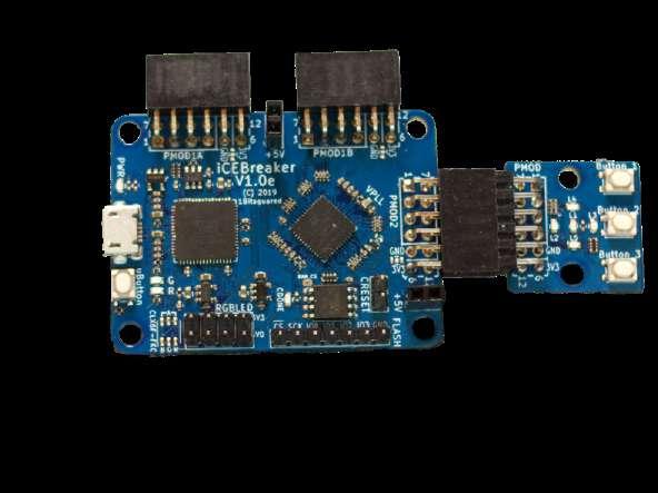
For our purposes you will not need to design a PCB for the FPGA. The iCEBreaker FPGA board (Figure 5) and the iCEBreaker Bitsy (Figure 6) from 1BitSquared [6] are two open hardware dev boards on which the iCE40UP5K FPGA comes already mounted. Another option with open hardware is the UPduino V3.0 [7] from tinyVision.ai (Figure 7).
The NEORV32 project fully supports the UPduino V3.0 board and includes some additional sample projects. Any changes required for the iCEBreaker FPGA board can be carried out very quickly. To start off with we will use the UPduino V3.0 and then go on to show what needs to be adapted to our example project so that it runs on the iCEBreaker Board.
Using this FPGA gives you a SoC in with 64 kB space for applications, 64 kB RAM, SPI interface, I²C interface, 4 input and 4 output pins, 3 PWM pins and a UART, together with the RV32IMAC core running at 18 MHz.
The Toolchain
There are two paths you can take when it comes to selecting the toolchain for the Lattice iCE40up5k. We can install the tools from Lattice [8] or use the OSS CAD suite from YosysHQ [9] which is based completely on open source tools. For this project, we will choose the latter, open source route. In this case it means Ubuntu 20.04 LTS will be our operating system and the OSS CAD Suite will be used to synthesize the NEORV32 for the iCE40UP5K.
In addition to the tools for the FPGA, a demo program to run on the synthesized RISC-V processor will also be compiled later: A classic implementation of the ‘Hello World’ message will be sent out using the UART. Here, too, open source tools are used to generate a suitable tool chain (similar to that for the Kendryte K210 [10]). A GNU C compiler (GCC) and additional libraries for the NEORV32 peripherals are available.
Mise en Place
As my colleague Clemens Valens demonstrated in his video [11], working with FPGAs is a bit like preparing a meal. The first step is to make sure you have all the ingredients and necessary utensils (tools). If you don’t want to risk affecting your main operating system installation, you can also implement a virtual machine. A freshly installed version of Ubuntu 20.04 on an AMD64 system is the setup assumed here. The use of a Raspberry Pi should also be possible, since both Ubuntu 20.04 and the Raspberry Pi OS are based on Debian, but there may be small differences due to the architecture. For this project I used Ubuntu 20.04 running on an AMD64 machine only.
In order to synthesize the “hardware” for the FPGA, the current release of the OSS CAD Suite [12] needs to be downloaded into the home folder. This file is called oss-cad-suite-linux-x64-xxxxxxxx.tgz. In a terminal, this file is now unpacked using tar -xvzf oss-cad-suitelinux-x64-xxxxxxxx.tgz and then moved to /opt with sudo mv ~/oss-cad-suite /opt/. In order that the folder can be accessed later, the rights are set by using chmod 777 /opt/oss-cad-suite -R. The libgnat-9 library is also required which is installed with sudo apt install libgnat-9. The FPGA tools are now in place.
Compiler
Next we need the files associated with the NEORV32 [4] from the GitHub repository. To do this, we will install git by entering sudo apt install git. The NEORV32 repository is then cloned with git clone https://github.com/stnolting/neorv32.git ~/neorv32.
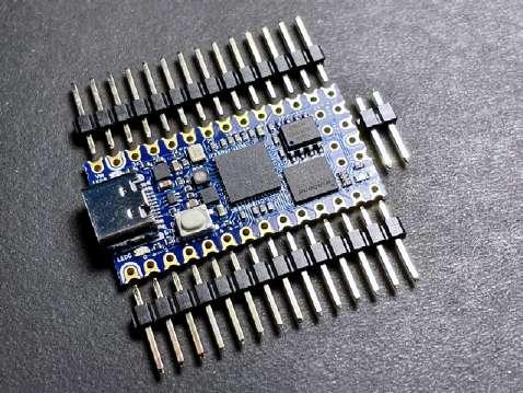
Figure 6: iCEBreaker Bitsy (Source: https://cdn.shopify.com/s/ files/1/1069/4424/products/IMG_3859_large.jpg / 1BitSquare). Figure 7: The UPduino V3.0 with pin header strips fitted.

So that we will be able to communicate with the NEORV32 later, a terminal program will be required. For this, I normally use HTerm by Tobias Hammer, which has proven to be a useful tool. This program can be downloaded from his homepage [13] with wget https:// www.der-hammer.info/terminal/hterm-linux-64.tgz. Now with mkdir ~/hterm && tar -xvf hterm-linux-64.tgz -C ~/hterm the contents of the tgz file will be extracted to the ~/hterm folder. So that the serial interfaces can be accessed later by a user, they must be added as a member to the dialout group. To do this use the terminal and enter sudo adduser $(whoami) dialout.
The C compiler itself now needs to undergo a process of compilation. In the examples for the iCE40up5k, the NEORV32 is configured as RV32IMAC, so that commands for integer multiplication and division are available (see also the RISC-V Naming Convention box). The compiler must be compiled in accordance with this particular architecture and the command extensions; you can read in the NEORV32 [14] documentation why this adaptation is important.
Using a terminal, first go to the home folder using cd ~ and enter git clone https://github.com/riscv/riscv-gnu-toolchain --recursive to clone the RISC-V Toolchain. We will also need some additional packages which can be installed using the following:
sudo apt-get install autoconf automake autotools-dev curl python3 libmpc-dev libmpfr-dev libgmp-dev gawk build-essential bison flex texinfo gperf libtool patchutils bc zlib1g-dev libexpat-dev
Finally, the compiler and libraries can be compiled.
With RISC-V CPU models a hierarchy exists in terms of the supported commands. This means that code compiled for an RV32I processor model will also be able to run on an RV32IMAC model, but not the other way around. Therefore, the recommendation is to first compile the toolchain so that it is compatible to the lowest common denominator model. Using the terminal, we can switch to the directory containing the cloned toolchain with cd ~/riscv-gnu-toolchain and then use ./configure --prefix=/opt/riscv --with-arch=rv32i --with-abi=ilp32 to preconfigure the toolchain for compiliation. Now we can start the compilation process using sudo make. The toolchain can then be found in /opt/riscv. So that everyone can access the compiler, the rights to of/opt/riscv need to be modified. Using a terminal you can grant everyone access with the command chmod 777 /opt/riscv -R.
For the OSS CAD Suite and the RISC-V GCC Toolchain, it is necessary to make a modification of the path variable in the /etc/enviroment file. Using sudo nano /etc/enviroment we can open the file and then after PATH=" enter the string /opt/oss-cad-suite/bin:/ opt/riscv/bin: and then save the file.
Most FPGA boards use an FT232H chip from FTDI to handle the programming interface. In order for a user to gain access to it without root rights, an appropriate udev rule must be created for the FTDI chip. Using the terminal enter sudo nano /etc/udev/rules.d/53lattice-ftdi.rules to open a new file for writing to. In this file it is necessary to enter:
ACTION=="add", ATTR{idVendor}=="0403", ATTR{idProduct}=="6010", MODE:="666" ACTION=="add", ATTR{idVendor}=="0403", ATTR{idProduct}=="6014", MODE:="666"
Then, save the file. The preparations are now complete and the synthesis and subsequent upload of our first test program can begin. A reboot should first be carried out so that all the settings take effect. Another recommendation is to install an editor with syntax highlighting for use with VHDL and Verilog.
NEORV32 for the FPGA
In its de-energized state, the FPGA is not configured. On power up, the iCE40UP5K reads the connection description from an external SPI flash. This description of the internal connections must first be stored into the SPI flash on the UPDuino V3.0 or the iCEBreaker.
In this article, we create a sample project for the UPduino V3.0 board, which contains the processor and peripherals. This creates a system that should be able to run directly on the FPGA.

Figure 8: Changes necessary to configure the RAM size.

Figure 9: NEORV32_exe.bin is created.
USB MOD2 CH340
Figure 10: Connections between the UPduino and the USB/serial adapter.
5V VCC 3V3
TXD
RXD GND 1
2
3
4
5
6
48 47 46 45 44 43 42 41 40 39 38 37 36 35 34 33 32 31 30 29 28 27 26 25
28 38 42 36 43 34 37 31 35 32 27 26 25 23 GND 3V3 5V B G R DONE RST VIO GND
50
49 5V GND
2 46 47 45 48 3 4 44 6 9 MOD1 Upduino 3.0
1 1 18 19 13 21 12 GND 12M USB
10 20 50 51 SCK 55
1 2 3 4 5 6 7 8 9 10 1 1 12 13 14 15 16 17 18 19 20 21 22 23 24
In a terminal you now have to change to the example directory for the open-source tools with cd ~/neorv32/setups/osflow/. In order to start the synthesis and thus the creation of the bit stream for the FPGA, we just need to enter make BOARD=UPduino UP5KDemo as a command, after that it can take a little while until the process of synthesis is complete. Now in the ~/neorv32/setups/osflow/ folder a file named neorv32_UPduino_v3_UP5KDemo.bit has been created. The bit stream contained in this file describes how the basic logic blocks must be interconnected in the FPGA. This bit stream now needs to be written into the SPI flash on the FPGA board.
Now we can hook up the UPduino board to the PC via a USB cable. In the terminal we enter iceprog ~/neorv32/setups/osflow/neorv32_ UPduino_v3_UP5KDemo.bit. This starts the programming of the external SPI flash, and the configuration is then loaded into the FPGA. This means that we now have a RISC-V system configured in the UPduino V3.0, which we can now supply with software.
As mentioned at the beginning, 64 KB of memory is available for applications and 64 KB is available as RAM. For the peripherals we have an SPI interface, I²C, a UART, four inputs and four outputs, as well as three PWM outputs. The CPU synthesized here is an RV32IMAC model that runs at 18 MHz. The SoC in the FPGA also has a small bootloader that can be accessed via the UART.
Hello World
The FPGA is now equipped with the NEORV32 and the first Hello World demo can be compiled and uploaded to the RISC-V. The NEORV32 is configurable so the current size of the RAM must be defined appropriately in the linker script. To do this, use the terminal to enter nano ~/neorv32/sw/common/neorv32.ld and in line 62:
ram (rwx) : ORIGIN = 0x80000000, LENGTH = DEFINED(make_bootloader) ? 512 : 8*1024
In exchange for:
ram (rwx) : ORIGIN = 0x80000000, LENGTH =
DEFINED(make_bootloader) ? 512 : 64*1024 (Figure 8)
The RISC-V compiler is now ready for use. In an open terminal you can go to the folder of the Hello World program by entering:
cd ~/neorv32/sw/example/hello_world
To generate an executable file that can be loaded into the NEORV32, you just need to enter make exe to generate the neorv32_exe.bin file (Figure 9). In order for the NEORV32 to be able to be executed, it should now be uploaded to the board. The integrated bootloader is used for this and receives data via the UART (19200 baud, 8 data bits, 1 stop bit, no parity, no flow control). If a UPduino V3.0 board is used, an external USB-to-serial converter will be required, such as the CH340-based one from the Elektor Store. (Refer to the Related Products text box.) This must be connected as shown in Figure 10.
HTerm is used for the upload itself. This can be started from a terminal with ~/hterm/hterm a window like in Figure 11 should appear. The USB-to-serial converter must now be selected as the port, which usually reports itself as /dev/ttyUSB0; depending on the hardware configuration and the selected adapter, however, this may be different.
After connecting to the USB serial adapter, the UPduino can be supplied with voltage and the bootloader message should be visible (Figure 12). If a character is not sent to the bootloader in time, it tries to autoboot from the SPI flash, which currently does not contain any software. Any character sent within 8 seconds of starting the bootloader will switch it into command mode. A u must then be sent to activate the upload in the bootloader and the Select File button must be clicked in HTerm. As can be seen in Figure 13, select the file neorv32_exe.bin in the ~/neorv32/sw/example/hello_world folder and then upload it. When everything is finished, the bootloader reports an OK as shown in Figure 14 and the program can be executed by entering e.

Figure 11: An open HTerm window.
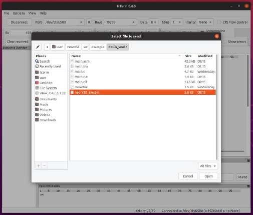
Figure 13: Dialog to upload neorv32_exe.bin. Figure 12: The NEORV32 bootloader.

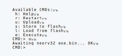
Figure 14: A successful upload.
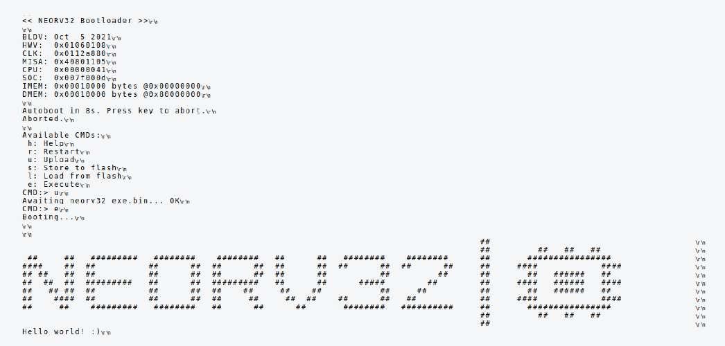
Figure 15: ‘Hello World’ from the NEORV32.
RISC-V Naming Convention
RISC-V is a generic term for the different architecture variants. Our Elektor colleague Stuart Cording wrote a nice article (“What is RISC-V,” Elektor 7-8/2021, [2]) in which the details are explained in more detail. RISC-V describes an ISA in which the processors are categorized as 32, 64 or 128 bit versions. A 32-bit processor has a designation that starts with RV32 for 32 bits, so that an RV64 indicates a 64-bit processor. In addition, after RV32 or RV64, there are a number of letters that indicate which commands and extensions the processor can handle. These letters range from A to Z; their meaning can be looked up in the current RISC-V specification [3]. The performance of the processors differ according to the supported commands and extensions.
The result can be seen in Figure 15. The program has not been stored in the SPI flash, but into the RAM-based “ROM” of the NEORV32. This extends the service life of the SPI flash by cutting down on the number of write cycles. The disadvantage of this configuration is that, each time the NEORV32 is restarted, the program needs to be uploaded again. If the program is to be loaded automatically, the bootloader must upload it to the SPI flash. In addition to the basic “Hello World” demo, there are other examples to discover, including a complete FreeRTOS, which has already featured in Elektor [15]. It is worth taking a look at the ~/neorv32/sw/example folder, where several other examples can be found in their own folders.
A New iCE40UP5K FPGA Environment
Using the iCEBreaker Board will demonstrate how the NEORV32 can also be adapted to other iCE40up5k boards. The features of the SoC itself are not changed here, but the pinout assignment on the FPGA is adapted so that an iCEBreaker board can be used and a suitable bit stream will be generated.
To do this, the Makefile in ~/neorv32/setup/osflow needs to be edited. The file is opened using your text editor of choice and the new board is added as the target. For the iCEBreaker board we write the following in line 72:
iCEBreaker: $(MAKE) \ BITSTREAM=neorv32_$(BOARD)_$(DESIGN).bit \ NEORV32_MEM_SRC="devices/ice40/neorv32_imem.ice40up_ spram.vhd devices/ice40/neorv32_dmem.ice40up_spram. vhd" \
This ensures that the board is referenced in the primary Makefile. Also in ~/neorv32/setup/osflow/boards an iCEBreaker.mk file with the following contents is required:
.PHONY: all
all: bit echo "! Built $(IMPL) for $(BOARD)"
The Makefiles are thereby prepared but two VHDL-files are still missing. In ~/neorv32/setup/osflow/board_tops/ the files neorv32_iCEBreaker_ BoardTop_UP5KDemo.vhd and neorv32_iCEBreaker_BoardTop_ MinimalBoot.vhd must be generated. Since their contents are almost identical to that of the neorv32_UPduino_BoardTop_UP5KDemo.vhd and neorv32_UPduino_BoardTop_MinimalBoot.vhd files, they can just be copied and renamed. This should be done using a terminal and entering:
cp ~/neorv32/setups/osflow/board_tops/neorv32_UPduino_
BoardTop_MinimalBoot.vhd ~/neorv32/setups/osflow/board_tops/neorv32_iCEBreaker_
BoardTop_MinimalBoot.vhd
And:
cp ~/neorv32/setups/osflow/board_tops/neorv32_UPduino_
BoardTop_UP5KDemo.vhd ~/neorv32/setups/osflow/board_tops/neorv32_iCEBreaker_
BoardTop_UP5KDemo.vhd
A few changes need to be made to the two files neorv32_ iCEBreaker_BoardTop_UP5KDemo.vhd and neorv32_iCEBreaker_ BoardTop_MinimalBoot.vhd. In file neorv32_iCEBreaker_ BoardTop_UP5KDemo.vhd must line 42 in entity neorv32_ iCEBreaker_BoardTop_UP5KDemo is and line 68 in architecture neorv32_iCEBreaker_BoardTop_UP5KDemo_rtl of neorv32_ iCEBreaker_BoardTop_UP5KDemo is be changed. In the file neorv32_iCEBreaker_BoardTop_MinimalBoot.vhd line 42 in entity neorv32_iCEBreaker_BoardTop_MinimalBoot is and line 54 in architecture neorv32_iCEBreaker_BoardTop_MinimalBoot_ rtl of neorv32_iCEBreaker_BoardTop_MinimalBoot is are to be changed. The last step is for the iCEBreaker.pcf ConstraintsFile to be placed in ~/neorv32/setups/osflow/constraints/. The contents of the file can be seen in Listing 1. ICEBreaker.pcf defines which function should be routed to which pin of the FPGA. This also directly integrates the USB/serial converter, which is on the iCEBreaker board, and routes the buttons and LEDs on the IO pins of the NEORV32. One thing that is missing is the reset button. Even though it is already defined in the constraints file, its function is not referenced here.
With all the necessary changes made, we can generate a bit stream just like we did with the UPduino board. For this we need a terminal and enter cd ~/neorv32/setups/osflow to get to the osflow folder. Using make BOARD=iCEBeaker UP5KDemo we can start the make process. To upload the bitstreams to the iCEBreaker (just like we did in the UPduino) we can use iceprog ~/neorv32/setups/osflow/ neorv32_iCEBreaker_UP5KDemo.bit.
Uploading the software for the NEORV32 is also taken care of by the integrated bootloader. Using this board we will not need an external USB/serial converter; instead, we use the second channel of the converter integrated on the iCEBreaker board.
A Reset Button for the NEORV32
To restart the NEORV32, the power supply needs to be briefly disconnected and then reconnected. This gets to be a bit annoying eventually, and since the iCEBreaker has enough buttons, one of them can be
Listing 1: iCEBreaker.pcf
#UART (uart0) ldc_set_location -site {9} [get_ports uart_txd_o] ldc_set_location -site {6} [get_ports uart_rxd_i]
#SPI - on-board flash ldc_set_location -site {14} [get_ports flash_sdo_o] ldc_set_location -site {15} [get_ports flash_sck_o] ldc_set_location -site {16} [get_ports flash_csn_o] ldc_set_location -site {17} [get_ports flash_sdi_i]
#SPI - user port ldc_set_location -site {43} [get_ports spi_sdo_o] ldc_set_location -site {38} [get_ports spi_sck_o] ldc_set_location -site {34} [get_ports spi_csn_o] ldc_set_location -site {31} [get_ports spi_sdi_i]
#TWI ldc_set_location -site {2} [get_ports twi_sda_io] ldc_set_location -site {4} [get_ports twi_scl_io] #GPIO - input ldc_set_location -site {18} [get_ports {gpio_i[0]}] ldc_set_location -site {19} [get_ports {gpio_i[1]}] ldc_set_location -site {20} [get_ports {gpio_i[2]}] ldc_set_location -site {28} [get_ports {gpio_i[3]}]
#GPIO - output ldc_set_location -site {25} [get_ports {gpio_o[0]}] ldc_set_location -site {26} [get_ports {gpio_o[1]}] ldc_set_location -site {27} [get_ports {gpio_o[2]}] ldc_set_location -site {23} [get_ports {gpio_o[3]}]
#RGB power LED ldc_set_location -site {39} [get_ports {pwm_o[0]}] ldc_set_location -site {40} [get_ports {pwm_o[1]}] ldc_set_location -site {41} [get_ports {pwm_o[2]}]
#Reset ldc_set_location -site {10} [get_ports {user_reset_btn}]
used as a reset. We can use the uButton near the micro-USB socket on the board, which is connected to pin 10 of the FPGA.
The NEORV32 has an internal reset input which is connected to the “lock” output from the system PLL. When the PLL goes out of lock, it issues a reset to the NEORV32. The cleanest solution would be to gate the user reset signal from the button together with the lock signal so that either would issue a reset to the NEORV32. The quick and dirty solution is to just use the reset input of the PLL. Figure 16 shows the connection of the uButton with this input. Now when the PLL is reset, the NEORV32 is also reset, since the lock_o signal goes low when PLL is reset.
In order to incorporate this change into the UP5K-demo project, it will be necessary to insert one line and then make a change to another line in the neorv32_iCEBreaker_BoardTop_UP5KDemo.vhd file residing in the ~/neorv32/setups/board_tops folder. After line 44, insert the new line user_reset_btn : in std_ulogic;. Line 130 now needs to be changed to RESETB => user_reset_btn,. Be careful, a syntax error will occur if you forget the comma at the end. The uButton is now configured to function as a reset. Finally, to make the changes, a new bit stream must be generated in the UP5K-Demo and loaded into the iCEBreaker FPGA.
Outlook
No doubt we could dedicate a whole book on the subject of RISC-V, FPGA, and also the NEORV32. The iCE40UP5K is an inexpensive choice for beginners, if only the chip were more widely available. The two boards used in the article are not the only ones that use this FPGA.
Figure 16: Connection of the uButton reset to the PLL reset input.

There is at least a handful of other platforms. From the Raspberry Pi add-on to the complete handheld console, many options are available. The various tools and projects applicable to this FPGA are also worth investigating. Examples are LiteX [16], with which your own SoC can be put together like in a construction kit and is not necessarily limited to RISC-V, the RISCboy [17] by Luke Wren, who provides a Gameboy-like system in the FPGA, and the OK-ice40-PRO [18] gamepad console.
Should the procurement situation improve, there will certainly be additional projects and ideas for the iCE40UP5K. A small games console built using an iCE40UP5K together with a Raspberry Pi RP2040 already seems to be in the pipeline [19].
210175-01
Contributors
Text and images: Mathias Claußen Editor: Jens Nickel Translation: Martin Cooke Layout: Harmen Heida
Questions or Comments?

Do you have any technical questions or comments relating to this article? Contact the author at mathias.claussen@elektor.com or contact the Elektor team at editor@elektor.com.
RELATED PRODUCTS
> Alchitry Cu FPGA Development Board (Lattice iCE40 HX) (SKU 19640) www.elektor.com/19640
> CH340 USB to TTL Converter UART Module CH340G (3.3 V/5.5 V) (SKU 19151) www.elektor.com/19151
> M. Dalrymple, Inside an Open-Source Processor (Elektor 2021) (SKU 19826) www.elektor.com/19826
WEB LINKS
[1] M. Ossmann, “The SCCC project (1),” Elektor 3-4/2019: https://www.elektormagazine.com/magazine/elektor-88/42444 [2] S. Cording, “What is RISC-V,” Elektor 7-8/2021: http://www.elektormagazine.com/magazine/elektor-179/59732 [3] RISC-V Specification: http://riscv.org/technical/specifications/ [4] NEORV32 GitHub Repository: http://github.com/stnolting/neorv32/ [5] Lattice iCE40UltraPlus Product page: http://www.latticesemi.com/en/Products/FPGAandCPLD/iCE40UltraPlus [6] iCEBreaker GitHub Repository: http://github.com/icebreaker-fpga/icebreaker [7] UPduino GitHub Repository: http://github.com/tinyvision-ai-inc/UPduino-v3.0 [8] Lattice Radiant: http://www.latticesemi.com/LatticeRadiant [9] YosysHQ oss-cad-suite-build : http://github.com/YosysHQ/oss-cad-suite-build [10] Setup a toolchain for the Kendryte K210, Elektor Labs: http://www.elektormagazine.com/labs/setup-a-toolchain-for-the-kendryte-k210-1 [11] Linux-flavored Snickerdoodles with Zynq, ElektorTV: http://www.youtube.com/watch?v=EE4yYZ-FEoQ [12] YosysHQ oss-cad-suite-build Releases: http://github.com/YosysHQ/oss-cad-suite-build/releases [13] HTerm: http://www.der-hammer.info/ [14] NEORV32 - Build the Toolchain from scratch: http://stnolting.github.io/neorv32/ug/#_building_the_toolchain_from_scratch [15] W. Gay, “Practical ESP32 Multitasking,” Elektor 1-2/2020: http://www.elektormagazine.com/magazine/elektor-139/56997 [16] LiteX: http://github.com/enjoy-digital/litex [17] RISCBoy : http://github.com/Wren6991/RISCBoy [18] OK-iCE40Pro Handheld: http://github.com/WiFiBoy/OK-iCE40Pro [19] PicoStation3D: http://github.com/Wren6991/PicoStation3D [20] Nolting S., The NEORV32 RISC-V-Processor, GitHub repository 2020: http://raw.githubusercontent.com/stnolting/neorv32/master/docs/figures/neorv32_processor.png


