6 minute read
Correlative Surface Analysis - Enabling a More Detailed Understanding of Surfaces
Correlative Surface Analysis - Enabling a More Detailed Understanding of Surfaces Source: By Dr. Cameron Chai and Dr. Kamran Khajehpour, AXT Pty Ltd
There are many examples of where multiple materials characterisation techniques can and should be combined to give a comprehensive analysis. Often a single technique may have a shortcoming that can be overcome by correlating data from another technique, and the resultant datasets can be married together to provide a better understanding of the structure and properties of a material. Surface analysis is no exception.
Surface Analysis
The study of surfaces is important to a vast number of fields, including but not restricted to adhesion, contamination, coatings wettability, corrosion, chemical and catalytic activity, electrical, biocompatibility, etc. The surface is generally referred to as the top 1nm of the sample, which equates to just a few atomic layers, but is the place where materials react with their surrounding environments and is therefore of importance to our understanding of how materials behave.
In this article we look at a host of surface analytical techniques and how they can work together to provide a more comprehensive analysis. It should also be noted that, in all cases, the surface sensitive nature of these techniques relies on a clean surface in order to produce accurate results.
X-Ray Photoelectron Spectroscopy (XPS)
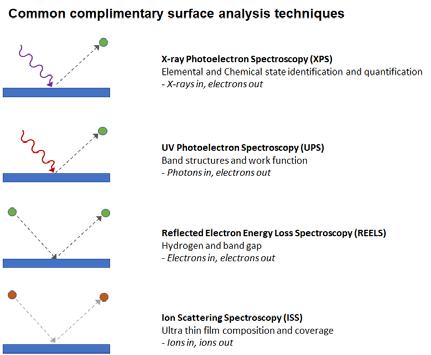
XPS is the most widely used surface analytical technique. With increasing focus on characterisation of surfaces and behaviour at the surface or interface, XPS is growing in popularity.
Exploiting the photoelectric effect, it relies on electrons being emitted from a material as a result of being irradiated by X-rays, and often requires an electron beam to compensate for positive charge build-up from X-ray irradiation. It generates signals from the outermost 10nm of the sample
It is a very capable analytical technique on its own. Using XPS imaging, potential problem areas can be located visually so users can zero in on points of interest to analyse. It can also produce depth profiles using the MAGCIS gas cluster ion source which can be used to etch away layers, which can be subsequently analysed using XPS.
Sometimes XPS can not provide all the answers, and other techniques are required to derive a more complete picture that can better help explain the behaviour of a material or component.
Ultraviolet Photoelectron Spectroscopy (UPS)
UPS is similar to XPS except that it uses UV photons generated by a (helium, argon or neon) gas discharge lamp to irradiate the sample. This technique is just as surface sensitive as XPS, and UPS acesses the valence levels associated with chemical bonding and electronic properties of materials, producing data that enables the determination of molecular species. UPS generates spectra from the valence band region and as such is used for valence band acquisition and workfunction measurement.
Reflection Electron Energy Loss Spectroscopy (REELS)
REELS is an excellent complementary technique to XPS, as it provides three main areas of interest. Firstly, it can help determine band gap (the difference in energy between the valence and conduction bands) which is particularly important for semiconductor analyses. Secondly, it gives much richer information with regards to loss features, as compared to XPS. And thirdly it can be used to confirm the presence of hydrogen in the surface region.
REELS uses a beam of electrons of known energy (typically 1000eV) to elastically scatter electrons from the top few nm of the sample. By detecting the energy of the scattered electrons, and plotting these on a kinetic energy scale, any energy loss of the scattered electrons can be determined. It is this energy loss that yields a lot of information such as band gap.
Unlike XPS, REELS is sensitive to hydrogen. As such, it can be used to compare differences in hydrogen content between samples.
Figure 1. Band gap measurements using REELS data. Both samples are Al 2 O 3 coatings on SiO 2 , 0.8nm thick with band gap of 6.9eV (left) and right 4nm thicj with band gap of 6.5eV.
Ion Scattering Spectroscopy (ISS)
ISS is similar to REELS in that the sample is bombarded by an ion beam of known energy. The difference here is the ions are typically noble gases such as He+, Ne+, Ar+ etc., where the ion should be lighter than the atoms in the sample. It again relies on measuring the kinetic energy of backscattered ions.
The impinging ions lose an amount of energy during collision with atoms on the surface, and the amount of energy lost is dependent on the mass of the atom involved in the collision. Any ions that penetrate are unable to be detected, meaning that ISS exclusively analyses the top layer of atoms, making it very surface sensitive.
While ISS is generally regarded as non-destructive, it can also be used for depth profiling by increasing the mass of the ions and the ion current. This effectively etches the surface, similar to XPS
depth profiling. The process is called dynamic ISS, and uses cycles of high energy to remove material and low energy ISS to analyse the surface.

Figure 2. ISS spectrum of SiO 2 , with beam energy calibrated against a gold standard.

Raman Spectroscopy
Raman involves shining a laser onto the surface of the sample. Most light will bounce back elastically, while some will scatter inelastically, undergoing a change in energy according to the Stokes shift principle, resulting in a slight change in colour and wavelength.
The scattered Raman light is emitted upon transition of a molecule from a higher energy virtual state to a lower vibrational energy level. Different wavelength lasers can be used to access different vibrational modes in a variety of samples. Raman is principally used for providing molecular structure information that is complimentary to the chemical composition information provided by XPS.
Multiple Surface Analysis Techniques in One Instrument
Nexsa, from Thermo Scientific, can provide up to five techniques on one system, each directed to the same analysis position, enabling in-situ analysis of the same region of the same sample using any or all of the techniques including XPS, UPS, Raman, ISS (or LEIS) and REELS. The system is flexible and expandable having been optimised for multi-technique surface analysis.
System control and data handling is seamlessly integrated in the Avantage data system. Avantage provides access to all of the analytical modes, including inbuilt tools for determining bandgap from REELS spectra.
In days gone by, the running of XPS experiments, and analysing the resultant data, was the realm of highly trained technicians. Modern intuitive user interfaces like Avantage make surface measurements much simpler, allowing novice users to accurately analyse the data. This brings another suite of analytical techniques well within reach of more researchers.
Case Study – Gate Dielectric Material
Gate dielectrics are used in components such as MOSFETS, a type of field effect transistor (FET). Silicon substrates FETs commonly use SiO 2 as the gate dielectric. As the gate oxide thicknesses get smaller, the SiO 2 can be subject to excessive leakage. This can be combatted using a high dielectric layer such as HfO2 that can be deposited using processes such as Atomic Layer Deposition (ALD).
In this study, the properties of the HfO 2 coating are examined using complimentary techniques.
Figure 3. XPS analysis of a HfO 2 coating in a MOSFET device.
Case Study 2 – TiO 2 Polymorphs
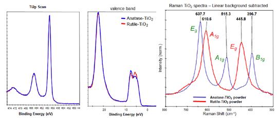
In this simple example, rutile and anatase samples, both TiO 2 polymorphs, were examined by XPS and Raman. The XPS spectra are both identical, as expected as they both have the same chemical composition. However, when examined using Raman, the two different phases can be readily distinguished.
Figure 4. (a) and (b) are portions of the XPS spectra, while (c) is the Raman spectra for rutile and anatase.


