










Plus: How Embedded Power Electronics Are Stopping Coastal Erosion Development Kit Selector http://embeddedcomputing.com/designs/iot_dev_kits/ resource guide 2022 PG 18 FALL 2022 | VOLUME 20 | 2 | EMBEDDEDCOMPUTING.COM SEALEVEL SYSTEMS, INC. 12009 COM Express Compact Type 6 Evaluation Board PG 21 Every Penny Counts in Embedded Design PG 6 PG 14 AVNET EMBEDDED Game-Changer for Ultra-Compact Embedded Compute from Avnet Embedded PG 24


November 15–18, 2022 Driving sustainable progress. Get your ticket now! electronica.de/tickets The future needs embedded systems. Networked solutions at electronica 2022.
EMBEDDED COMPUTING BRAND DIRECTOR Rich Nass rich.nass@opensysmedia.com
EDITOR-IN-CHIEF Brandon Lewis brandon.lewis@opensysmedia.com
ASSOCIATE EDITOR Tiera Oliver tiera.oliver@opensysmedia.com
ASSOCIATE EDITOR Taryn Engmark taryn.engmark@opensysmedia.com
ASSISTANT EDITOR Chad Cox chad.cox@opensysmedia.com
TECHNOLOGY EDITOR Curt Schwaderer curt.schwaderer@opensysmedia.com
MARKETING COORDINATOR Katelyn Albani katelyn.albani@opensysmedia.com
CREATIVE DIRECTOR Stephanie Sweet stephanie.sweet@opensysmedia.com
WEB DEVELOPER Paul Nelson paul.nelson@opensysmedia.com
WEBCAST MANAGER Ryan Graff ryan.graff@opensysmedia.com
EMAIL MARKETING SPECIALIST Drew Kaufman drew.kaufman@opensysmedia.com
SALES/MARKETING
DIRECTOR OF SALES Tom Varcie tom.varcie@opensysmedia.com (734) 748-9660
DIRECTOR OF SALES ENABLEMENT Barbara Quinlan barbara.quinlan@opensysmedia.com AND PRODUCT MARKETING (480) 236-8818
DIRECTOR OF MARKETING Eric Henry eric.henry@opensysmedia.com OPERATIONS & AUDIENCE DEVELOPMENT (541) 760-5361
STRATEGIC ACCOUNT MANAGER Rebecca Barker rebecca.barker@opensysmedia.com (281) 724-8021
STRATEGIC ACCOUNT MANAGER Bill Barron bill.barron@opensysmedia.com (516) 376-9838
STRATEGIC ACCOUNT MANAGER Kathleen Wackowski kathleen.wackowski@opensysmedia.com (978) 888-7367
SOUTHERN CAL REGIONAL SALES MANAGER Len Pettek len.pettek@opensysmedia.com (805) 231-9582
STRATEGIC ACCOUNT MANAGER Lesley Harmoning lesley.harmoning@opensysmedia.com
EUROPEAN ACCOUNT MANAGER Jill Thibert jill.thibert@opensysmedia.com
TAIWAN SALES ACCOUNT MANAGER Patty Wu patty.wu@opensysmedia.com
CHINA SALES ACCOUNT MANAGER Judy Wang judywang2000@vip.126.com
INSIDE SALES Amy Russell amy.russell@opensysmedia.com
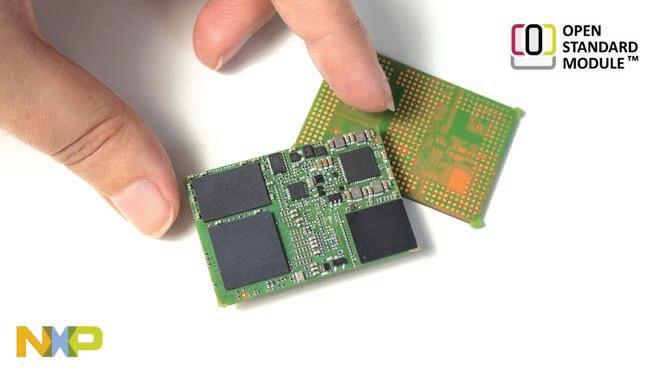
1 Avnet Embedded –Game-Changer for Ultra-Compact Embedded Compute from Avnet Embedded
1 Digi-Key Corporation –Development Kit Selector
2 electronica –November 15-18, 2022 –Networked Solutions at electronica 2022
17 Verotec –Commercial and Rugged System Components
1 SeaLevel Systems, Inc. –12009 COM Express Compact Type 6 Evaluation Board
36 Tadiran – IIoT Devices Run Longer on Tadiran batteries
2022 IoT Device Security Conference November 3, 2022 Register Now: iotdevicesecurityconference.com
RISC-V Summit December 12-15, 2022 San Jose Convention Center
PRESIDENT Patrick Hopper patrick.hopper@opensysmedia.com
EXECUTIVE VICE PRESIDENT John McHale john.mchale@opensysmedia.com
EXECUTIVE VICE PRESIDENT AND ECD BRAND DIRECTOR Rich Nass rich.nass@opensysmedia.com
VITA EDITORIAL DIRECTOR Jerry Gipper jerry.gipper@opensysmedia.com
MES ASSISTANT MANAGING EDITOR Lisa Daigle lisa.daigle@opensysmedia.com
TECHNOLOGY
EDITOR – WASHINGTON BUREAU Dan Taylor dan.taylor@opensysmedia.com
CREATIVE PROJECTS Chris Rassiccia chris.rassiccia@opensysmedia.com
MARKETING COORDINATOR Katelyn Albani katelyn.albani@opensysmedia.com
FINANCIAL ASSISTANT Emily Verhoeks emily.verhoeks@opensysmedia.com
SUBSCRIPTION MANAGER subscriptions@opensysmedia.com
CORPORATE OFFICE
1505 N. Hayden Rd. #105 • Scottsdale, AZ 85257 • Tel: (480) 967-5581
REPRINTS
WRIGHT’S MEDIA REPRINT COORDINATOR Kathy Richey clientsuccess@wrightsmedia.com (281) 419-5725
Jack Ganssle, Ganssle Group
Bill Gatliff, Independent Consultant
Andrew Girson, Barr Group
David Kleidermacher, Google
Jean LaBrosse, Independent Consultant
Scot Morrison, Siemens Digital Industries Software
Rob Oshana, NXP
Kamran Shah, Klick Health
www.embeddedcomputing.com Embedded Computing Design RESOURCE GUIDE | Fall 2022 3 PAGE ADVERTISER
SOCIAL EVENTS AD LIST WWW.OPENSYSMEDIA.COM Facebook.com/Embedded.Computing.Design @Embedded_comp www.linkedin.com/showcase/ embedded-computing-design/ www.youtube.com/c/ EmbeddedComputingDesign EMBEDDED COMPUTING DESIGN ADVISORY BOARD Ian Ferguson, Lynx Software Technologies
opsy.st/ECDLinkedIn


FEATURES
Every Penny Counts in Embedded Design
 By Shawn Prestridge, IAR Systems
Time-to-Market Using
Stack
By Paul Pazandak and Fabrizio Bertocci, Real-Time Innovations, Inc.
Narrowband-IoT Can Ruin Your Project
By Fabian Kochem, 1NCE
Vulnerabilities with SDRs
By Brendon McHugh, Per Vices
By Taryn Engmark, Associate Editor
By
COVER
A rough rule-of-thumb is that per-unit processor cost increases by about one US dollar each time you double the memory. Learn how compiler optimization techniques and a highassurance software stack can help you right-size your device designs, then discover how innovative power electronics are stopping coastal erosion and giving new life to coral reefs.

how innovative power electronics are stopping
2022 Resource Guide product profiles begin on page 18.
WEB EXTRAS
Embedded Insiders Podcast: Git-ing Started in the World of Agile/ DevOps Hardware Development
Listen Today: bit.ly/EmbeddedInsidersPodcast
How Accenture & Johnson Controls Are Curbing Climate Change with an Assist from Edge AI Read Now: embeddedcomputing.com/technology/ ai-machine-learning/how-accenture-johnsoncontrols-are-curbing-climate-change-with-anassist-from-edge-ai

White Paper: Considerations for Inductor Simulation Models
By Coilcraft
Download Here: embeddedcomputing.com/ technology/software-and-os/simulation-modelingtools/considerations-for-inductor-simulationmodels
Published by:

4 Embedded Computing Design RESOURCE GUIDE | Fall 2022 www.embeddedcomputing.com Fall 2022 | Volume 20 | Number 2 2022 OpenSystems Media® © 2022 Embedded Computing Design All registered brands and trademarks within Embedded Computing Design magazine are the property of their respective owners. ISSN: Print 1542-6408 Online: 1542-6459
CONTENTS
COLUMNS 5 TRACKING TRENDS How to Scale IoT Past Distributed Data Silos
Brandon Lewis, Editor-in-Chief 6
8 Accelerating
an Integrated High-Assurance Software
10 How MQTT on
12 Uncover RF Security
14 How Embedded Power Electronics Are Stopping Coastal Erosion
18 2022 RESOURCE GUIDE PROFILES 12
@Embedded.Computing.Design To unsubscribe, email your name, address, and subscription number as it appears on the label to: subscriptions@opensysmedia.com 14 10 bit.ly/ECDYouTubeChannel@embedded_comp www.instagram.com/embeddedcomputingdesign
How to Scale IoT Past Distributed Data Silos
By Brandon Lewis, Editor-in-Chief

To reduce latency, network utilization, and cost, many IoT deployments now store and analyze data at or near the edge node. But “distributed” can be a bad thing when it comes to data, particularly if it means informa tion gets trapped in silos across a network. So, what hap pens when you inevitably need it?
Let’s start at the data source. For data in motion, tech nologies built around publish-subscribe tenets were designed to deal with this type of environment. In a pub lish-subscribe network like MQTT or DDS, data related to a given topic is broadcast by a publisher across the network, and nodes on the network subscribe to that topic for updates. This promotes decentralized data net working that maps nicely to the evolution of IoT networks, as well as the broader network infrastructure considering 5G networks deploy 1.4-2x base stations compared to 4G to support the increase in edge workloads.
At their best, protocols like MQTT and DDS run over TCP or UDP in homogeneous environments with little-to-no packet loss and a high degree of endpoint fanout. This allows them to transmit messages from node to node at high speed with minimal overhead. But as tools for data in motion, what they don’t provide is a built-in, locationaware data retrieval mechanism as they were designed to push one message and move on to the next.
For data at rest, technologies like named-data networking (NDN) provide similar data centricity by allowing packets to be labeled something other than just their destination address. Packets, which can be named any thing, are cached in location-aware content stores that give users the opportunity to access them post-transmis sion by querying the designated label. However, NDN was designed as an Internet technology, which doesn’t fit well with the latency and resource-constrained envi ronments of many end applications.
Unifying Data in Motion and At Rest From Edge to Cloud
Since the inception of IoT, the goal has been to unify data distribution and retrieval architectures under a single enterprise-to-edge paradigm rather than patch together heterogeneous platforms and technology stacks. ZettaScale Technology was founded earlier this year to bridge the gap using a technology called Zenoh, a protocol that addresses data in transit, in use, and at rest by blending publish-subscribe architectures with geographically distributed storage.
Over peer-to-peer, routed, or mesh network topolo gies, the protocol broadcasts data to subscribers using a
“key expression,” which is essentially a string containing resource identifiers. For example, the key expression for a temperature sensor in room 42 on the second floor of the Louvre Museum in Paris would be something like: Louvre/2/42/sensor/temp. Unlike normal packets, this string is something a developer can understand and potentially query from a database. This leads us to the third Zenoh abstraction besides publishers and sub scribers: queryables.
Queryables contain all the values for a given key expres sion so the protocol can deposit any published data related to that expression into a data store. Correspondingly, this allows the network to be queried for data related to those queryables, and Zenoh supports a storage man ager plugin for integrating filesystems, databases, and the like so queries can be run on historical data as well. Zenoh supports push, pull, and get commands for use with its simple yet powerful semantics. Returning to our previous building example, all that a developer needs to retrieve the temperature information for all rooms on the second floor of the Louvre is issue a get command for Louvre/2/*/sensor/temp
Because Zenoh is publish-subscribe, results are retrieved from the nearest data store or node containing the information requested. The protocol also includes a data caching feature that allows sleeping nodes to pull whatever data they need from the nearest infrastructural node when required then return to sleep.
The Cost of Data Scalability
But features almost always come at a cost, and usually when you’re adding enterprise-class querying capabili ties to the edge that cost is in the form of performance, resources, or both. So how does Zenoh stack up with the pub-sub alternatives?
The protocol incurs a wire overhead of between just 4 and 6 bytes while being able to transmit up to 4 mil lion messages per second. When compared with MQTT and DDS, Zenoh has a 75 and 64 percent smaller wire overhead, respectively. According to ZettaScale, it also exhibits 40x the throughput performance of MQTT and 10x that of XRCE-DDS. Benchmark transport latency with the new protocol is just 35 µs. Zenoh works with IP transports, or Zigbee, Thread, or other edge data links, which it can even support in the same deployment. It truly is designed from the ground up for scalability.
You can find out just how far at https://zenoh.io/docs/ getting-started/key-concepts.
TRACKING TRENDS brandon.lewis@opensysmedia.com
www.embeddedcomputing.com Embedded Computing Design RESOURCE GUIDE | Fall 2022 5
Every Penny Counts in Embedded Design
By Shawn Prestridge, IAR Systems
Do more with less – this phrase, which captures Buckminster Fuller’s concept of ephemeralization, caught fire in the embedded space in the 1990s but never seems to go out-of-fashion. Managers constantly squeeze budgets and schedules to deliver products faster and cheaper, often with quality suffering as a result. Let’s explore techniques that will help developers find and fix defects more quickly, help save money on build material lists (BML), and perhaps avoid the challenges of ephemeralization. While the primary focus is on Arm-based cores, many of these techniques are directly applicable to other cores as similar functionality exists in many embedded devices.
On most embedded designs, the two most expensive parts are often the screen (if the device has one; most IoT devices do not), and the processor. As you add more memory (flash and RAM) to a processor, the cost of the processor increases. A rough rule-of-thumb is that the per-unit processor cost increases by about $1 USD each time you double the memory.
What makes this problem worse is that embedded engineers are often not very good at forecasting memory requirements during the design phase of an application. These best “guess timates” on the amount of memory needed are key factors in the processor selection. Given that many production runs are in the hundreds of thousands or millions of units per year, adding an unnecessary dollar to the BML has a deleterious impact on the company’s bottom line.
As a result, innumerable projects “run tight on resources,” which is code for “we didn’t forecast our memory needs correctly.” What exacerbates this problem is that BMLs are often pitched to upper management towards the beginning of the project. Once this happens, the cost becomes inviolable. This leaves people scrambling to reduce the memory footprint or leaning on procurement to keep the BML costs the same as management expects by negotiating better prices on other components. To lower the memory footprint, teams often turn to their compiler’s optimization engine to reduce the size of the generated code.
Raising the Bar for Compiler Optimization
Some engineers are exceedingly reluctant to crank up the opti mization because they perceive that optimization introduces bugs into the system. This is rarely the case, and in my experi ence, about 5 percent of optimization issues turn out to be a problem with the optimizer. When the optimization level is raised, the compiler gets extremely picky about the semantics of the C and C++ language. The optimization decisions are made based upon a strict interpretation of the language rules. Often, engineers are not fully aware of all the nuances of the language and code in a way that seems natural to them.
For example, if a function call is written like this:
myFunc(varA, varB, varC, varD);
The natural assumption is that the variables will be read from left to right: varA will be read from memory, then varB, etc. However, there is nothing in C or C++ that says this has to be the case. If the memory is laid out either purposefully or by happenstance where varB is next to varD, then a high optimi zation might use an index register to read successive memory spaces to save on code size and speed.
In most cases, this will not make a difference to the code. However, if you are depending on the variables being accessed as they have been written, from left to right, then a situation may occur where the code runs fine at lower optimization but not at high levels. This is where a good support structure from your tools vendor can help with spotting these types of prob lems and rewrite sections of code to optimize better and work correctly, independent of the optimization settings.
Moreover, if your code can work the same at high optimization, it’s written correctly and is better-tested. If the code does not work at higher optimizations, there is a good chance that a latent defect is waiting to “bite you.”
Good tools can save 10-40 percent on code size when set for high size optimization. However, not all optimization transfor mations are good choices for any piece of code – some trans formations might actually increase code size on certain types of code.
There are resources available that address “getting the least out of your compiler,” meaning the smallest size code and lowest execution time. Saving this amount of code space can be the difference between stripping out functionality to stay within a device’s size, missing schedules due to hand-optimizing your code, or going over-budget on the BML.
RESOURCE-CONSTRAINED ENGINEERING
6 Embedded Computing Design RESOURCE GUIDE | Fall 2022 www.embeddedcomputing.com
While good code can operate the same at any level of optimi zation, debugging highly-optimized code is tricky at the very best. For example, entire sections of code can be folded into other sections of code in a completely different place. This is why it is essential to debug your code at low or no optimization and to verify the code is functioning correctly before increasing the optimization to run the full battery of tests.
Debugging Cost Out of the BML
Part of what makes embedded debugging difficult is most people simply don’t know of all the debugging tools in their arsenal. They tend to default to printf statements and code breakpoints. These defaults don’t help when trying to isolate a hard fault, find where a stack overflow is occurring, or why a variable keeps getting clobbered. The good news is exceptional tools exist that help find these types of problems.
Let’s start with the hard fault. Many modern MCUs have live instruction trace capabilities that allow you to follow the instruction flow. On Arm-based devices, the technology used to accomplish this is Embedded Trace Macrocell (ETM). If the device supports ETM, pull the trace pins to your debug header and use a trace-enabled debugger, such as the IAR I-jet Trace, that can capture that live instruction flow and show it in the debugger window.
To find what caused the hard fault, simply scroll through the trace window and find the instruction that executed before you went to the fault handler. Voila! That instruction is the culprit. If the bug can be reliably reproduced, set a breakpoint at the fault handler and eliminate all the scrolling in the trace window – the culprit is the penultimate instruction in the trace window.
Now the cause is known, so a breakpoint can be set on the culprit and run through the test case again to see what’s wrong with your code that’s causing the exception.
But what if you don’t have ETM? Most Arm-based devices have Serial Wire Output (SWO) that allows for a sampled, low-speed trace. While you do not get every single instruction, this can pro vide enough trace information to narrow down and locate the problem. Additionally, try to derate the MCU clock and/or adjust the SWO settings to get a finer granularity of trace information out of the debugger to hone in on where the problem occurs.
Other device architectures have similar functionality to ETM or SWO. Therefore, using high-quality tools can leverage that information and quickly isolate and eradicate the problem. Additionally, available support resources help wring extra per formance out of the SWO to secure more trace data.
Stop Stack Overflows and Clobbered Data
How about a stack overflow or finding out why a variable mysteriously loses its contents? Use the same technique to diagnose both of these conditions.
In the Arm universe, most processors have a Data Watchpoint and Trace (DWT) block in their debug interface that can be used to quickly isolate these types of issues. In this case, use a data watchpoint to find out where the bad stuff is happening. This watchpoint is essentially a breakpoint whenever a piece of data gets touched.
Configure the options to only break execution if the data is read from, written to, or both. Furthermore, even restrict it to only breaking if the data is a specific value with a certain bit mask. This is quite handy when avoiding it from stopping each and every time that data gets accessed.
In the case of the stack overflow, we want to set a data watch point at the top of the stack. It does not matter if reading or writing to that value because the stack is already blown at that point in code. The processor will halt execution at the top of the stack, providing a fully preserved call stack that allows for visibility into which piece of code is blowing the stack as well as how you arrived at that point. This is key to determine how to fix the bug.
With clobbered data, we use essentially the same technique, just setting a data watchpoint if that variable experiences a write. If it is always clobbered with the same value, narrow the breakpoint further to only trip when that value is written to the variable. Then, run our test case one more time and find out whose code is causing the issue.
Again, many other architectures have similar functionality that can be used to effect the same results. With high-quality tools, finding these types of issues becomes easier and increases the odds of meeting an aggressive schedule and deadline.
Let Procurement Know You Care
Doing more with less may seem to be a contradiction, but it can be easily accomplished by using the right tools. By using compiler optimizations, you can shoehorn your code into the smallest possible space in order to use the least expensive device for your application.
Optimization can also help desk-check your code to see if it runs the same at high optimization to find potential code defects before you check it into a build (and thus make every defect count against your release metrics). It also helps you debug more efficiently by using your full toolbox to find bugs more quickly, thus shortening the test-and-fix cycle and getting your project out the door faster.
If you know what tools are in your toolbox (and how to use them properly), you can make every penny count for your organization.
Shawn Prestridge is a Senior Field Application Engineer & US FAE Manager at IAR Systems.
RESOURCE-CONSTRAINED ENGINEERING YOUTUBE www.youtube.com/c/IARSystems/featured IAR Systems www.iarsystems.com TWITTER @iarsystems LinkedIn www.linkedin.com/company/iar-systems www.embeddedcomputing.com Embedded Computing Design RESOURCE GUIDE | Fall 2022 7
Accelerating Time-to-Market using an Integrated High-Assurance Software Stack
By Paul Pazandak and Fabrizio Bertocci, Real-Time Innovations, Inc.
General-purpose computing, operating systems (OSs), inherent language features (like C memory allocation), and software quality issues have led to a lack of inherent security and resiliency in systems throughout industry. This has resulted in many security breaches that have had dire consequences to national security. It is necessary to design assured systems based on appropriate techniques and tools by applying sound security and engineering principles.
Generally speaking, building an assured system entails a thorough understanding of the problem domain, deep analysis of domain-specific work flows and requirements, careful archi tectural considerations and design trade-offs, vetted development, proper configuration, and managed deploy ment of the final product. This level of care will also be needed throughout the product lifecycle.
Specifically related to system architec ture, leveraging hardware and software techniques and tools for enhanced security boils down to applying sound security principles to suitable targets such as memory access (for example, the Principles of Open Design, Least Privilege, Separation of Privilege, and Complete Mediation). Other research and develop ment efforts may adopt different applica tions of such principles to their particular environments and design goals.
The process of building trustworthy and high-assurance systems is complex, costly, and requires significant exper tise. The end goal is to create a com plete software-hardware solution whose components (both individually and col lectively) meet your customers’ required levels of assurance for safety and secu rity. This will vary depending upon the standards that are required.
For example, RTCA DO-178C for flight safety airworthiness and ISO 26262 for
autonomous vehicles each contain multiple levels of certification corresponding to the level of criticality (the role) that the component has. Within DO-178C, for instance, there are five levels:
› Level A (Catastrophic): Prevents continued safe flight or landing, many fatal injuries
› Level B (Hazardous/Severe): Potentially fatal injuries to a small number of occupants
› Level C (Major): Impairs crew efficiency, discomfort, or possible injuries to occupants
› Level D (Minor): Reduced aircraft safety margins, but well within crew capabilities
› Level E (No Effect): Does not affect the safety of the aircraft at all
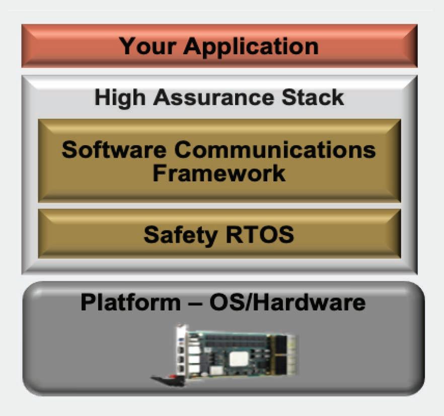
It is simply too costly in terms of funding and time to build a high-assurance system from top to bottom. On the contrary, the goal should be to develop as little code as possible. The more proven/certifiable code that one can acquire or license, the less one will need to design, develop, maintain, and certify. This will expedite develop ment efforts and significantly lower costs. A high-assurance software stack provides this (Figure 1).
The role of this stack is to provide a proven foundation. It is composed of a real-time operating system (RTOS) that has been verified or certified (a safety RTOS) and a distributed communications middleware.
Foundations of a High-Assurance Software Stack
For the last six years, under DARPA research funding, RTI has been working on a verified stack for embedded systems to accelerate safety/security accreditation. In this stack we use RTI’s certifiable Connext Software Framework. RTI Connext sup ports the Object Management Group Data Distribution Service standard (OMG DDS). Connext is running in nearly 2,000 critical systems today spanning avionics/defense, autonomous systems, medical robotics, energy, and industrial systems. Utilizing the OMG DDS open standard enables the ability to rapidly assemble loosely coupled (distributed) software components into a working system.
For the Safety RTOS we chose the open-source seL4 separation kernel. It is a mathe matically provably correct microkernel that will provide both time and space separation between running processes. It guarantees that there will be no unintended data leakage between processes, and that one process cannot impact the operation of another.
RESOURCE-CONSTRAINED ENGINEERING
8 Embedded Computing Design RESOURCE GUIDE | Fall 2022 www.embeddedcomputing.com
Figure 1 | A high-assurance software stack allows engineering organizations designing safety-critical systems to develop as little code as possible.
This provides greater system resilience and security, which are also attributes of a multiple independent levels of security (MILS) solution.
Derivatives of seL4 are being used by several large technology companies today.
The Need for a Secure Microkernel
To understand the need for a secure microkernel like seL4, it is helpful to start with a closer look at kernel design prin ciples in general.
There are two main kernel design approaches – the monolithic kernel and the microkernel. In the former, all code required for providing typical OS services is directly implemented in the kernel itself. The kernel executes in the privileged mode of the hardware, meaning that all code is granted unrestricted access and control of all system resources.
This type of implementation might be beneficial to the overall system perfor mance, but it can lead to dangerous situations if any of the kernel compo nents feature some type of malfunc tion – a state that could be exploited by an attacker. A prominent example is provided by the Linux kernel, which –containing more than 20 million lines of code – can be expected to contain a cer tain number of bugs providing potential attack channels.
In contrast, the microkernel design copes with this drawback by drastically reducing the trusted computing base (TCB), meaning the subset of code in the overall system that must be trusted to operate correctly. A microkernel follows the design principle of having the kernel contain only the most fundamental mechanisms (for example, inter-process communication and scheduling). All remaining OS functionality must be transferred to the unprivileged user mode, thereby running encapsulated within isolated sandboxes.
This approach protects the kernel processes from any interference from the outside, only allowing communication that is explicitly wanted. For a well-designed micro kernel like seL4 this means that the code base can be reduced to the order of ten thousand lines of code. This drastically shrinks the attack surface.
seL4 and DDS: A Reliable Combination
The purpose of seL4 is to provide a reliable, safe, and secure foundation for applica tions that require it. This includes, for example, military systems, medical devices, robotics, autonomous vehicles, and energy systems. Without exception, these highassurance applications require a reliable and robust distributed communications capa bility, which is not provided by seL4.
OMG DDS for Real-Time Systems is a real-time, secure, loosely coupled, publish/ subscribe software connectivity framework for distributed systems and is ideally suited as the communications layer for high-assurance systems, including for any safety RTOS such as seL4. While there are other open-source and commercial off-the-shelf commu nications framework technologies, those frameworks lack high-assurance certification and at best they provide rudimentary all-or-none security.
For DDS, seL4 creates an enriched, lower cost, smaller footprint, high-assurance foun dation. For seL4, DDS provides an open standards-based communications protocol.
DDS drastically simplifies seL4 inter-component/application development, reduces associated costs, and promotes component interoperability in the seL4 development community. DDS is a solution that will standardize data distribution in a more consis tent, secure, and efficient manner. It provides a publish-subscribe model that enables easier, faster, and more secure distributed system development. Application devel opers can be alleviated from the burden of creating their own piecemeal, perhaps pro prietary, and one-off solutions for message-based communications and deciphering the message sequence, allowing them to focus on domain-specific components and rely on DDS to provide standardized, secure interaction with other (local and remote) entities in the system.
Reducing Barriers to Entry for High-Assurance Software
DDS will significantly reduce the barriers of entry for companies and developers that decide to use seL4/CAmkES because it provides an abstraction layer that hides most of the complexity associated with developing applications on top of seL4. DDS will significantly reduce the development time and the need for seL4 subject matter expertise in-house.
To get started, we have provided links to a number of general resources about seL4 and DDS below.
Paul Pazandak is Director of Research at RTI.
Fabrizio Bertocci is Principal Systems Engineer at RTI.
RESOURCE-CONSTRAINED ENGINEERING
EMAILS paul@rti.com and fab@rti.com YOUTUBE www.youtube.com/user/RealTimeInnovations Real-Time Innovations (RTI) www.rti.com TWITTER @rti_software LINKEDIN www.linkedin.com/company/rti www.embeddedcomputing.com Embedded Computing Design RESOURCE GUIDE | Fall 2022 9
How MQTT on NarrowbandIoT Can Ruin Your Project
By Fabian Kochem, 1NCE
MQTT is a popular protocol for connecting the Internet of Things (IoT). But it’s incompatible with Narrowband-IoT (NB-IoT) – an increasingly popular communications standard for most IoT projects. It works fine during prototyping, giving companies the false impression that MQTT is the right choice of protocol.

But chances are high that products using MQTT will suffer performance issues or completely malfunction when they’re in the field. This problem is exacerbated by the fact that many manufacturers and system integrators aren’t aware of the consequent risks: high-expense support efforts, the need to reengage development teams, problems in distributing firmware updates to the device fleet, and product recalls.
NB-IoT is a cellular technology for constrained, (often) battery-powered devices that falls into the Low-Power Wide-Area (LPWA) networking category. It promises low cost, long battery life, and superior coverage compared to more tra ditional standards such as LTE. It’s ideal for asset tracking, smart metering, smart city, and other connected devices that require little data (such as geographical posi tioning, sensor data, or error codes) and is already being used in real-world applica tions with deployments increasing daily.
NB-IoT networks are currently operating in 64 countries (including the U.S., China,
Australia, and the majority of Europe), and 166 operators worldwide are investing in expanding this reach. But despite its benefits, there remains an unadvertised poten tial snag that, if it not caught early in product development, could prevent a stable product lifecycle of 10 years or more.
NB-IoT Works Differently Than the Rest of the Internet NB-IoT is optimized for the User Datagram Protocol (UDP), but most of the Internet uses the Transmission Control Protocol (TCP) for basic communication. TCP is a good choice for certain projects such as websites, file downloads, and emails because it guarantees that data arrives, that it’s in the right order, and allows for error detection and retransmission in case of corruption.
But TCP requires more processing power on the device itself, leading to more energy consumption, and it consumes more traffic. If your device wants to send a single byte (for example, that a light is on or off, sent in the form of a 1 or 0), the overhead of TCP metadata is another 40 bytes. In practice, data is rarely sent in single bytes, but it’s
IOT NETWORKING
10 Embedded Computing Design RESOURCE GUIDE | Fall 2022 www.embeddedcomputing.com
worth noting because cellular data trans missions are a heavy energy consumer that must be minimized on batterypowered devices.
Worse yet, if there’s radio interference from other devices, if the device is in an area with poor reception like a base ment, or data gets lost or corrupted, the retransmission mechanisms of TCP kick in and much more data is consumed. These scenarios are quite common in cellular networks, which means that devices send entire packets again which amounts to twice the traffic and twice the energy.
These characteristics make TCP a bad choice for battery-powered devices or constrained hardware. As NB-IoT is optimized for constrained devices, the 3GPP standardized it around global UDP instead.
Traps When Using MQTT on NB-IoT
Many product manufacturers pick MQTT as the data exchange protocol between device and cloud because it is widely supported by cloud providers and IoT application enablement platforms. They also often pick MQTT simply because they’ve used it when developing pre vious connected products based on Wi-Fi or LTE.
But MQTT relies on TCP’s error correc tion and retransmission schemes and works well with Wi-Fi, LTE, and Ethernet. It’s not that TCP is incompatible with NB-IoT, but when companies are experimenting with the technology (for example, when building a prototype) they’re working in conditions that don’t reflect what the device will encounter later in its deployment lifecycle.
So, MQTT and TCP work great if you have “good enough” network coverage. And because most offices are not under ground and/or are in big cities with a lot of radio coverage where issues are minimal, many companies assume that MQTT will work automatically for their specific use case. After all, the prototype was successful, but they unknowingly release a subpar product to the market.
Then, once deployed, they start receiving complaints from customers having issues because they were unaware of the consequences of placing an NB-IoT-enabled device in a basement with bad reception, for example.
Like any bit of tech, TCP connections can and will fail, resulting in repeated data retransmissions. This leads to wasting traffic on overhead other than actual business data, less battery life, and poor user experience.
And there’s another ticking time bomb for projects using TCP: The more crowded NB-IoT networks become, the more often TCP connections will fail. So even if compa nies optimize their devices for bad local reception, performance will degrade over time.
Addressing the Business Impact
What seemed like a good product launch at first is now potentially bound for disaster. High latency leads to a bad user experience and, depending on the use case, could completely derail a project. Then end users rightfully complain that their device isn’t working as expected.
Consequently, the development team must be reassembled or a new team without prior knowledge of the system must be formed to make improvements. Then the new solution has to be rolled out, which is tricky for a device that’s offline because it means either the customer has to return the product or a technician must be dispatched to the device’s location to perform upgrades. However it’s addressed, this process incurs significant time and monetary expense.
Another small factor in this complex equation is the cost associated with data over ages, as the used traffic might exceed contractually agreed upon limits and trigger additional charges from carriers. The amount depends on the contract, carrier, and size of device fleet, but this can’t be ignored, either.
But the biggest cost of all is a dissatisfied customer base. It’s hard to measure the impact this sort of scenario has on their loyalty or impression of a brand, but it could have long-lasting consequences.
Protocols Actually Optimized for NB-IoT
To be fair, most of the points outline above are true for all connected devices and not limited to MQTT on NB-IoT. Nevertheless, it’s a bigger problem here because busi nesses just aren’t aware of the risks – they’re simply too comfortable with MQTT to know what they’re missing
Product manufacturers and system integrators should choose UDP-friendly protocols such as CoAP or Lightweight M2M (LwM2M) instead. These protocols are optimized for cellular IoT and bring most of the advantages of TCP to UDP. These protocols all support data retransmission, error detection, and order guarantees. Additionally, LwM2M offers far more extensive features than MQTT in building connected prod ucts, especially constrained devices.
With these NB-IoT-friendly protocols designed in, companies and engineering teams can embark on extensive testing that examines how devices operate under various conditions in the field. This testing must cover many environments and every country rollouts are planned in, but that’s time and resource that might have been spent debugging the MQTT over NB-IoT problem, anyway.
Fabian Kochem is a product manager at 1NCE, flat-rate connectivity for IoT and M2M applications.
IOT NETWORKING
FACEBOOK www.facebook.com/1NCEGmbH YOUTUBE www.youtube.com/channel/ UCPU43V8FO5Ml3QWlfQs-eYg 1NCE www.1nce.com/en-us TWITTER @C1NCE_IoT LINKEDIN www.linkedin.com/company/1nce www.embeddedcomputing.com Embedded Computing Design RESOURCE GUIDE | Fall 2022 11
Uncover RF Security Vulnerabilities
with SDRs
By Brendon McHugh, Per Vices
In today’s wireless and 5G era, companies and individuals encounter a rising number of security threats on their IT assets. Wireless RF signals can be intercepted by anyone with low-cost radio equipment and decoded using open-source software, thus it’s imperative to assess connected designs for security vulnerabilities. This includes conducting penetration tests, jamming, replay attacks, and other methods to assess vulnerabilities in IoT RF protocols like Bluetooth, ZigBee, 6LoWPAN, Z-Wave, etc.
IoT device communications vary. Take the smart home, for example. Many systems will transmit directly to a gateway using a technology like ZigBee. Others will talk directly to nearby nodes over protocols like Bluetooth Mesh. Others still will leverage some type of backhaul straight to the cloud.
Nevertheless, there are similarities. For example, all of the topologies mentioned above describe a wireless network implementation, which means they all uti lize the RF spectrum.
Even in its simplest sense, modern RF communications networks are built on some of the most sophisticated engi neering in the world. That said, they’re still susceptible to a range of common threats, vulnerabilities, and attack vec tors, including spoofing, replay, tam pering, elevation of privilege, information disclosure, and Denial of Service attacks.
IoT threat models have evolved to help technologists and engineering organiza tions simulate and thwart such attacks. These models examine how external entities, processes, data flows, and data stores interact with and within a system, then offer defenders the ability to probe or penetration test the system for weaknesses.
For connected device developers dealing with multiple wireless systems or multiple wireless technologies within the same system, software-defined radios (SDRs) can pair with open software tools to provide a flexible, efficient, and cost-effective means of testing different protocol implementations for vulnerabilities.
But first, a brief primer on SDRs.
How SDRs Can Help Identify IoT Security Threats & Vulnerabilities
Software-defined radios contain a radio front-end (RFE) and digital backend. They function as a transceiver with onboard DSP capabilities, as well as a connection or connections to external systems for further processing, storage, and monitoring. The RFE provides receive (Rx) and transmit (Tx) functionality over a wide tuning range.
The highest performance SDRs contain:
› 3 GHz of instantaneous bandwidth using multiple independent channels, DACs, and ADCs
› FPGAs with onboard DSP capabilities for modulation, demodulation, upconverting, and down-converting
IOT NETWORKING
12 Embedded Computing Design RESOURCE GUIDE | Fall 2022 www.embeddedcomputing.com
The highest instantaneous bandwidth SDRs have a backhaul/data throughput of 4 x 100 Gbps over QSFP+ transceivers, which can be hooked up to external equipment or systems for further data storage, monitoring, or processing.
SDRs for Penetration Testing
As mentioned, penetration testing is a security practice where the security expert tries to find vulnerabilities in a computer system. The purpose of this exercise is to iden tify weak points in a system’s defenses that attackers could misuse.
The SDR-based Network Observation Utility Toolkit (SNOUT) leverages an SDR to passively sniff and interact with common IoT protocols. It provides a flexible and interactive framework for transmitting and receiving packets across different wireless protocols, enabling scanning or transmission through its adaptable command line.
SNOUT is built as an abstraction layer above the low-level signal transcoding pro cesses required for SDR-based communication. To provide interoperability with existing tools and facilitate advanced packet handling, SNOUT utilizes well-known software packages like GNU Radio, scapy-radio, and specialized SDR software. SNOUT performs device enumeration, vulnerability assessment, advanced packet replay, and packet fuzzing.
Mahony et al. explored the benefits of SDRs for IoT data analysis and penetration testing by implementing various intrusions using the signal processing block-based software Simulink/GNU Radio[1]. They uncovered the main security vulnerabilities of existing wireless sensor networks (WSNs) by adopting the ZigBee protocol and using SDRs as both WSN/IoT analysis tools and penetration testers concerned with external interference scenarios. The SDR provided IQ samples for analysis – even when packets were erroneous – and produced matched protocol interference.
The key advantage of SDRs over traditional packet sniffers is the received samples in the presence of strong channel interference.
Replay Attacks
A replay attack is a network attack in which a valid data transmission is fraudulently repeated or delayed. It is carried out either by the originator or by an adversary who intercepts the data and retransmits it, possibly as part of a spoofing attack by IP packet substitution. This is one of the lower tier versions of a man-in-the-middle attack.
Replay attacks are usually passive in nature, re-transmitting a previously captured raw PHY-layer payload or synthesizing a new frame based on decoded data.
The PHY layer is the lowest layer in the communication stack. In wired protocols it is voltage, timing, and wiring defining 1s and 0s. In wireless protocols it’s a pattern of energy being sent over an RF medium.
Replay attacks with an SDR are realized by:
1. Recording the signal with the SDR
2. Demodulating and decoding with a program in binary
3. Converting the binary to hex (0x)
4. Replaying with RFcat libraries
Using an SDR to collect and reverseengineer protocols can help you analyze various threats and make recommenda tions on how to improve security.
For example, the Z-wave routing pro tocol for IoT can be reverse-engineered to expose its vulnerabilities. Badenhop et al. conducted a black hole attack on an IoT network and showed that frames were silently discarded for a given source and destination[2]. The black hole attack was used to prevent sensor reports or actuating commands between the controller and devices, inhibiting the functionality of the IoT automation system.
Mitigating Attacks and Defenses with Various IoT Security Schemes
Yes, data encryption provides a security layer, in comparison with hardcoded or default passwords, but, as illustrated, modern RF attack vectors have the potential to circumvent those protec tions and PKI in general.
SDRs can efficiently uncover IoT vulner abilities that result in stronger overall security. And, when paired with the right tools, connected device developers have a ready-made penetration test har nesses that can accelerate their time to robust IoT security.
Brendon McHugh is a field applications engineer at Per Vices. Brendon is responsible for assisting current and prospective clients in configuring the right SDR solutions for their unique needs. He holds a degree in theoretical and mathematical physics from the University of Toronto.
References:
[1] O’Mahoney, G. D., Harris, P. J., & Murphy, C. C. (n.d.). Analyzing using software defined radios as wireless sensor network inspection and testing devices: An internet of things penetration testing perspective. IEEE Xplore. Retrieved September 15, 2022, from https://ieeexplore.ieee.org/ abstract/document/9119606
[2] Badenhop, C. W. (n.d.). A black hole attack model for reactive ad-hoc protocols. AFIT Scholar. Retrieved September 15, 2022, from https://scholar.afit.edu/etd/1077
› Data packetization over Ethernet optical links containing VITA49 IQ data in the Ethernet Stack
IOT NETWORKING
YOUTUBE www.youtube.com/channel/UC5gmiwvyzDwPpbqn5kNYPsQ Per Vices www.pervices.com TWITTER @PerVices LINKEDIN www.linkedin.com/company/per-vices-corporation www.embeddedcomputing.com Embedded Computing Design RESOURCE GUIDE | Fall 2022 13
Success Story: How Man-Made Coral Reefs Are Stopping Coastal Erosion
 By Taryn Engmark, Associate Editor
Off the coast of the Yucatán Peninsula lies the Mesoamerican Reef, which, like all coral reefs, is one of the most biologically diverse ecosystems on the planet. However, rising temperatures across the globe are affecting marine life just as much as terrestrial life. As seas get warmer, ocean acidification increases, and oxygen levels in the water drop, coral reefs like the Mesoamerican Reef are experiencing a fatal health crisis known as “white syndrome,” a disease that can kill corals in under 40 days.
FIGURE 3: The current supplied to the artificial reef structures enables the formation of rock to protect the steel from corrosion and provide secure attachment for coral polyps.
POWER ELECTRONICS IN ACTION 14 Embedded Computing Design RESOURCE GUIDE | Fall 2022 www.embeddedcomputing.com
But the effects of this disease aren’t limited to the corals themselves, or the marine life that relies on the reefs. Or even the ocean.
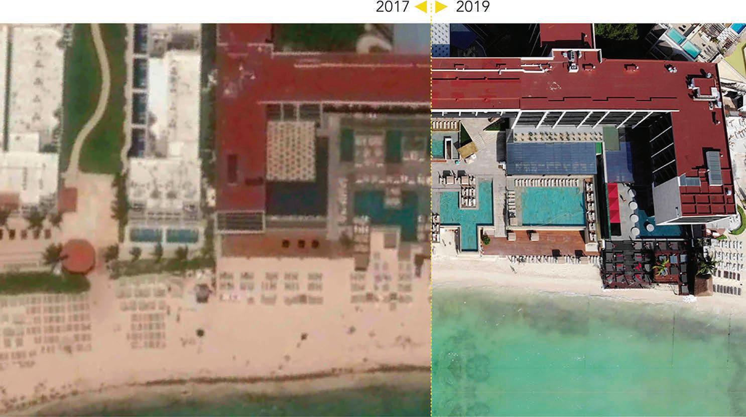
Reefs serve as a barrier between pow erful ocean waves and the beaches of coastal cities and structures. Without the reefs to impede the perpetual energy of the tides, waves are crashing onto shore at full force and rapidly eroding the coastlines of popular beaches (Figure 1).
But humans have discovered a way to help rebuild those dying coral reefs in an effort to preserve what remains of those beaches. CCell Renewables, a U.K.-based company working around the globe to prevent – and even reverse – coastal ero sion, developed a strategy to accelerate coral growth on submerged steel struc tures using a process called electrolysis.

How to Grow Your Own Coral Reef CCell has spent many months working on pilot projects in Cancún and Telchac, which lies on the northern coast of the Yucatán. The reef project is designed to mimic the natural growth conditions of coral reefs, which, on their own can take hundreds of years to reach maturity.
With CCell’s artificial reef structures, this process can occur in as little as 36 months.
“What’s crucial here is that you can’t just put those corals on plain sand, they’ll just sink into the sand and disappear,” says Dr. Will Bateman, CEO of CCell. “What we’re doing is providing almost like a backbone on which they can be placed.”
The foundation of the artificial reef is a series of 2.2-meter steel, half-tunnel cage-like structures (Figure 2). These structures are electrified by preciselycontrolled 1.2 to 6V electrical currents that run through a small metal anode. The cathode – in this system, is the reef structure itself – increases the pH levels of surrounding water, which causes salts to dissolve against the steel surface of the cage.
Oxygen produced by the anode’s lowlevel voltages combines with the soluble
effects of the cathode to enable the formation of aragonite (calcium carbonate) and brucite (magnesium hydroxide) rocks that attach to and seal the cages, protecting them from corrosion (Figure 3).
This entire process is dependent on precision voltage control between the remotely managed anodes and cathodes. If insufficient voltage is applied, the rock formations can become spongy and unsuitable for the hatchery-grown corals. You can imagine what too much electricity would do in this environment.
In a single month, a 3-5mm layer of rock can form over the structure. But even if rock successfully bonds to the steel cage so that divers can place local coral polyps by hand, the work isn’t done. CCell’s electrolysis process must continue for the attached corals to grow at the 3-5x accelerated rate needed to form mature reefs in three years.
“The last thing we want to be doing is continuing to grow rock when that process is happening, because we end up entombing the poor little coral polyps,” Bateman said.
CCell’s team has had to learn to interpret environmental conditions in the water to determine when a reduction – or even complete cease – of power input is warranted to slow the expansion of rock and maximize coral growth.
In some areas, beaches are shrinking by as much as one meter every six months.
FIGURE 1
Artificial reef structures are submerged along the Telchac coastline to impede wave energy and preserve beaches.
FIGURE 2
www.embeddedcomputing.com Embedded Computing Design RESOURCE GUIDE | Fall 2022 15
Delivering Power to Man-Made Reefs
Power for the CCell electrolysis process is generated by multiple sources. Some of it is drawn from conveniently-renewable resources courtesy CCell’s own wave-energy converter, which powers an electricity-producing hydraulic system with a paddle. Depending on wave conditions, this system can produce a range of voltage levels between 35V and 70V, which is then converted, controlled, and monitored by the electrolysis system itself.
Bigger pilots, like the one in Telchac, garner supplemental power from solar energy. With only a couple hundred watts available, smaller pilots, like those in Cancún, can’t harvest enough renewable energy and source their power from other means.
Sources aside, the power gathered must be transmitted to electrolysis systems at the pilot reef sites. This is achieved through a power delivery network (PDN) consisting of a front-end conversion regulation stage and a downstream point-of-load (PoL) regulation stage that delivers power to the electrolysis system over a cable.
But, as stated, the amount of power delivered to the system must be finely controlled. To maintain the peak current of 10A and 50W of power required for each length of reef, CCell leveraged Vicor’s Factorized Power Architecture that integrates a pre-regulation module (PRM) buck-boost voltage regulator and voltage transformation module (VTM) current multiplier with fast transient response (Figure 4). The PRM inputs unregulated voltage and outputs regulated voltage, which is used to drive the VTM.
“The VTM is, alternatively, a current multiplier,” says Philip Simpson, a field application engineer at Vicor. “A VTM acts as though it’s effectively a DC/DC converter.
OpenSystems Media works with industry leaders to develop and publish content that educates our readers.
A Path Forward for the Resource-Constrained Edge, Part 1
By SECO Electronics S.p.A.

Most edge computing applications today implement a computing platform capable of gathering data, communicating it via a network to a datacenter, via the “cloud” for complex processing, and providing local interaction via a humanmachine interface. In these use cases, a powerful local processor, often with artificial intelligence or image processing accelerators, with vast local interfacing capability to sensors and control mechanisms is required. PICMG’s new COM-HPC® specification, along with Intel’s latest Core and Xeon processors, enables this new set of products in a modular approach that minimizes hardware design effort and therefore development and time-to-market.
https://embeddedcomputing.com/technology/iot/edge-computing/ a-path-forward-for-the-resource-constrained-edge-part-1

“They’re a DC-to-DC transformer, conceptually, with what we call a K factor, which is equivalent to a turns ratio in a transformer-type application,” he continues. “The combination of the PRM and VTM gives you the ability to take reasonably high-voltage DC and convert it to quite low-voltage DC at relatively high current, but in a very efficient way.
“The combination of PRM and VTM that CCell are using gives efficiencies well over 90 percent,” Simpson explains. “It acts as an ideal transformer.”
In Cancún, 50 such control units are currently deployed along 120 meters of reef.
The Power to Reverse Effects of Global Warming
So far, the results are encouraging, with wave attenuation at the test sites projected to improve to 30 percent in the next year. For context, while global wave energy has increased by 0.41 percent annually as a result of global warming, just a five to eight percent reduction in
Check out our white papers at www.embedded-computing.com/ white-paper-library


POWER ELECTRONICS IN ACTION
16 Embedded Computing Design RESOURCE GUIDE | Fall 2022 www.embeddedcomputing.com
wave energy would restore the near-shore wave climate to levels from almost two decades ago.
The shape and porous structure of CCell’s artificial coral reefs work to stop larger waves from crashing onto the shore but allow smaller waves that deposit sand on beaches to pass through and rebuild what’s been lost.
There are currently plans to extend the artificial reefs by another 1 km along the Yucatán coast.
However, just as coastal erosion is not a phenomenon unique to one geographical area, CCell’s goals are not confined just to Mexican coasts. The company has been working on artificial reef structures in Israel, the Maldives, and elsewhere, all to stop – and hopefully reverse – erosion taking place across more than half the Earth’s coastlines.
Future goals for CCell include a potential partnership with Cornell University to implement acoustics on the reef structures that would mimic the sounds of living, thriving reefs to help attract marine life to the project sites.
Resources:
To learn more about CCell Renewables, visit: https://www.ccell.co.uk.
To get involved with CCell’s ongoing projects and contribute to their efforts, visit www.ccell.co.uk/crowdfunding.
For more information about Vicor’s Factorized Power Architecture, visit www.vicorpower.com/ industries-and-innovations/factorized-powerarchitecture.
To learn more about coastal erosion, visit https://toolkit.climate.gov/topics/coastalflood-risk/coastal-erosion.
2022 IoT Device Security Conference
November 3rd, 2022
You will get hacked. It’s no longer a question of “if.” It’s a question of “when.” But more importantly, what happens when the inevitable occurs is more important than ever. Your data, your network, and your finances must remain safe, regardless of what your end application is.
At the 2022 IoT Device Security Conference, we will look at security from every possible angle, focusing on three key verticals: automation, automotive, and consumer/mass market.
Register at www.bigmarker.com/series/ iot-device-security-virtual-conference/
thermal


Verotec
 Front
Vicor’s Factorized Power Architecture (FPA) utilizes a PRM buck-boost voltage regulator and a VTM to send power to CCell’s electrolysis system.
FIGURE 4
VIRTUAL EVENT Ph: 203-745-3537 • sales@verotec.us • verotec.us VERO Electronic Enclosures
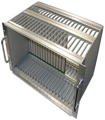
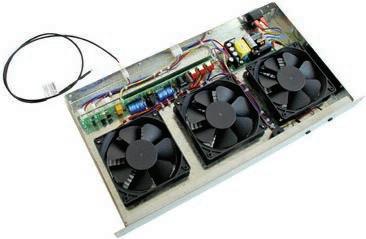
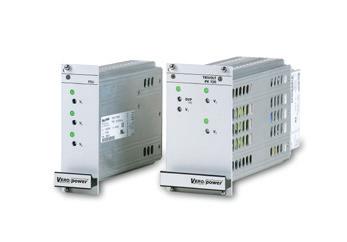
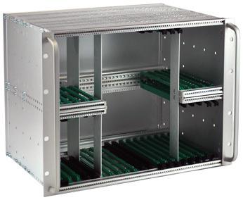
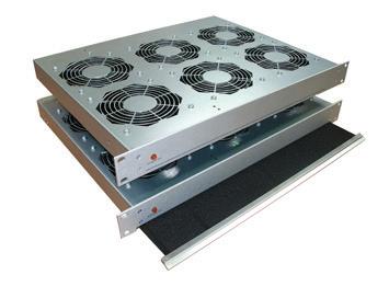
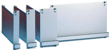
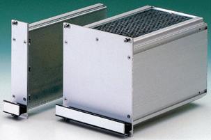
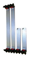
are specialists in the design, manufacture and integration of electronic enclosure products. For over 50 years the name VERO has been synonymous with engineering excellence and product quality. With facilities in the UK and US, Verotec continues that tradition. 3u to 9u ieee 1101.10 and ieee 1101.10/11 Card Cages C ommer C ial and rugged system C omponents
panels and modules supplies
solutions
www.embeddedcomputing.com Embedded Computing Design RESOURCE GUIDE | Fall 2022 17
The 2022 Embedded Computing Design Resource Guide showcases solutions for developers of industrial controls, edge computing, autonomous machines, and more.
DEVELOPMENT & EVALUATION KITS
SeaLevel Systems, Inc. 21
EDGE AI & MACHINE LEARNING
ADLINK Technology Inc 18-19 SECO USA 19-20
EMBEDDED PROCESSING: ARM
Lauterbach, Inc. 31
EMBEDDED PROCESSING: X86
ADLINK Technology Inc 35
EMBEDDED HARDWARE
Avnet 22-25 congatec 26 embeddedTS 25, 27 Kontron 28 Lauterbach, Inc. 28, 29 Opal Kelly 30 SECO USA 29
MEMORY & STORAGE
Apacer Memory America Inc. 32
INDUSTRIAL AUTOMATION & CONTROL
Peak System Technik 33-35
DLAP-401-Xavier Edge AI Platform
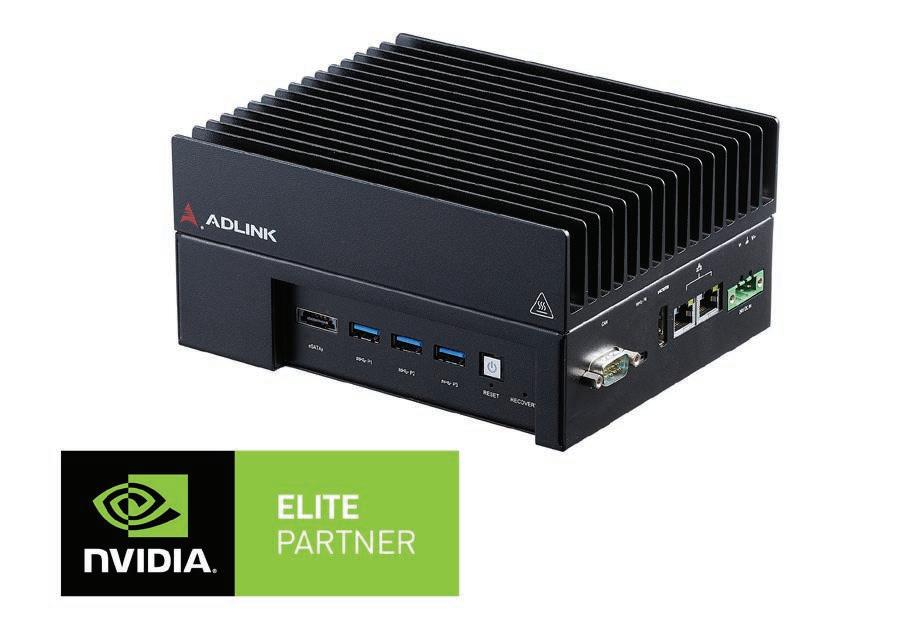
The ADLINK DLAP-401-Xavier Edge AI Platform integrates an NVIDIA® Jetson AGX Xavier™ SOM in a compact, fanless and durable package, designed to empower industry-leading smart automation across a wide range of applications. The DLAP-401-Xavier features intelligent, flexible, and robust computing power to automate intralogistics workflows in industrial and commercial environments alike.
Boasting comprehensive industrial I/O and visual inferencing capabilities all in this solid system, the ADLINK DLAP-401-Xavier Edge AI Platform supports 1x HDMI display, 2x GbE ports, 3x USB 3.1 ports (plus a USB 3.1 Type-C OTG port for software updates), 1x eSATA port, 1x isolated CAN bus, 1x M.2 NVME/SATA (for additional storage options), and 1x M.2 slot for the Wi-Fi communications.
durable and fanless design for 24/7
variety of industrial I/O ports and visual inferencing
integrated for remote device management
DLAP-401-Xavier?utm_source=ecd&utm_medium=directory&utm_campaign=aati-ecd-dlap
+1-800-966-5200
ADLINK_Tech
2022 RESOURCE GUIDE Embedded Computing Design
Edge AI & Machine Learning ADLINK Technology www.adlinktech.com info@adlinktech.com
www.linkedin.com/company/adlink-technology @
FEATURES: Ą Deep learning acceleration with NVIDIA® Jetson™ AGX Xavier SOM Ą Linux® Ubuntu operating system Ą High performance yet energy efficient Ą Support wide operating temperature Ą Compact,
operation Ą Wide
capabilities Ą Allxon
https://www.adlinktech.com/Products/Deep_Learning_Accelerator_Platform_and_Server/Inference_Platform/
18 Embedded Computing Design RESOURCE GUIDE | Fall 2022 www.embeddedcomputing.com
Express-TL, COM Express Type 6 Basic Size Module
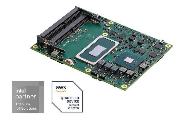
AI, machine learning and internet of things (IoT) devices increase demand for real-time processing – from the edge to the cloud. The ADLINK Express-TL module offers advanced tuning controls, immersive graphics, and unmatched connectivity, which allows new possibilities for AI, workload consolidation, and other intensive computing demands. ADLINK’s Express-TL COM Express Type 6 Basic size module is based on the 11th Gen Intel® Core™, Xeon® W and Celeron® 6000 processor, and is the first COM Express module to support PCI Express x16 Gen4, effectively doubling the bandwidth of previous generation COM Express modules. With a combined 8 cores, 16 threads, and up to 128GB memory, the Express-TL brings uncompromised system performance and responsiveness to your solution.
Featuring brand new Gen 12 Intel® UHD Graphics and Intel® AVX-512 Vector Neural Network Instructions (VNNI), the Express-TL provides AI inferencing performance as much as 3X higher compared to previous generation non-VNNI platforms. The integrated Gen 12 Intel® UHD Graphics core can be configured to support one 8K independent display or four 4K independent displays (HDMI/DP/eDP). In addition, legacy display interfaces such as LVDS and analog VGA are still supported as build options.
Key features for today’s applications are support for 2.5 GbE and USB 3.2 with transfer rates of up to 10Gb/s that can transfer image data from cameras faster than previous generation products. Combined with 8 processor cores at 25W TDP, Intel® AVX-512 VNNI and Intel® UHD Graphics, the Express-TL is well suited for AI at the edge applications (AIoT/IoT).
FEATURES:
Intel® Tiger Lake-H Processors, up to 8 cores, integrated Intel® UHD Graphics (Xe architecture)
AI inference (AVX512 VNNI + Intel® UHD GFX)
Up to 128GB DDR4 SO-DIMM, non-ECC and ECC
3x DDI channels, 1x LVDS (opt. 4 lanes eDP), opt. VGA, up to 4 independent displays, 8K capable
PCIe x16 Gen4, 2.5GbE (TSN, build option)
Extreme Rugged operating temperature: -40°C to +85°C (build option, selected SKUs)
https://www.adlinktech.com/Products/Computer_on_Modules/COMExpressType6/Express-TL?lang=en&utm_ source=ecd&utm_medium=directory&utm_campaign=aati-ecd-tiger-lake
ADLINK Technology
www.adlinktech.com
info@adlinktech.com
www.linkedin.com/company/adlink-technology
+1-800-966-5200
@ ADLINK_Tech
Edge AI & Machine Learning
Scale your IoT/AI App to millions of devices with CLEA
CLEA, an extensive AI/IoT platform from SECO, easily connects edge electronic devices to the cloud and facilitates real time device monitoring, analytics, infrastructure man agement, predictive maintenance, secure remote software updates, and more.

CLEA turns data from connected devices into actionable insights. The platform enables full retrofitting of existing infrastructure, rapid integration, high-performance data orchestration, and quick and easy deployment of AI applications on a mass scale. CLEA scales to large numbers of connected devices – located in multiple places, across a variety of hardware platforms, performing different functions. Integration with exist ing infrastructure is simple, thus improving efficiency, accelerating time to market, and allowing companies to develop products and services with high added value in a very short time. Bottom line: CLEA significantly improves operational efficiency, ROI, and data monetization.
CLEA is both ready to use and customizable for applications ranging from small installations to large enterprise solutions. Predictive maintenance of machinery, sales trends forecasts analysis, monitoring of medical parameters, and augmented driving are examples of the wide variety of CLEA uses.
From vending to medical, from factory automation to energy management, CLEA is the one stop solution for joining industry 4.0 quickly and economically, unlocking new business opportunities and efficiencies.
FEATURES:
Device lifecycle management: CLEA manages OTA updates, remote debugging, blue/green app deployments and much more, with a strong focus on security.
Data orchestration: CLEA easily scales to large numbers of connected devices and exchanged messages. Configure and customize your data journey optimally for your business.
Deploy AI models everywhere: whether it’s a pre-trained model or your very own, CLEA enables you to easily deploy it at the edge or in the cloud, seamlessly.
Rich, featureful APIs: everything in CLEA is API based, both at the edge and in the cloud, you are in full control and can easily add new capabilities.
Open-source core: all core middleware CLEA components are open-source software.
sales.us@seco.com

www.linkedin.com/company/seco-spa/
+1-240-558-2014
Embedded Computing Design
SECO www.seco.com
https://clea.ai
Edge AI & Machine Learning
www.embeddedcomputing.com Embedded Computing Design RESOURCE GUIDE | Fall 2022 19
SECO Intelligence and Electronic Solutions

With 40+ years of expertise in edge computing design, system assembly, custom packaged product, and IoT software platforms, SECO enables its customers with full end-to-end solutions, from edge device hardware to fully integrated product with Artificial Intelligence (AI) that transforms business operations.

Edge computing
SECO provides a broad array of cutting-edge embedded comput ing building blocks through worldwide engineering design, manu facturing, and technical support excellence.
Off-the-shelf computer-on-module (COM) and single board com puter (SBC) products feature leading processing technologies (NXP, Intel®, Xilinx, AMD) compliant with major standards (SMARC, QSeven®, COM-HPC®, COM Express®, Pico-ITX, eNuc). Modular HMIs, rugged tablets, boxed PCs, communication gateways, and pay ment systems, complete SECO’s portfolio of off-the-shelf edge platforms. SECO also offers custom design and integration of electronic devices, built for reliability and robustness.
Featured Products
• ORION COM-HPC® Client Module Size A is enabled by 12th Gen Intel® Core™ (formerly Alder Lake – H series) processors, delivering outstanding graphics performance for automation and AI at the edge.
• COM Express® OPHELIA, based on AMD Ryzen™ Embedded V2000 SOC, merges high performance with compactness for graphic and compute demanding edge applications.
• Qseven® ATLAS SOM, SMARC HALLEY SOM, and the ICARUS Pico-ITX SBC leverage the Intel® Atom™ X6000E series (formerly Elkhart Lake) in AIoT applications.
• SMARC LEVY, SWAN, and LEXELL SOMs provide ARM-based computing with NXP’s i.MX 8 application processors.
Intelligent Platform Solutions
SECO edge computing solutions are enabled with intelligence via CLEA- an AI/IoT software suite that easily connects edge electronic devices to the cloud and facilitates real time device monitoring, analytics, infrastructure management, predictive maintenance, secure remote software updates, data orchestra tion, and more. AI can run autonomously on the edge device or
in conjunction with cloud computing services. CLEA facilitates busi ness growth by optimizing efficiency, strengthening productivity, and minimizing maintenance time and cost. SECO is the leader in offering edge, IoT, and AI technologies as an all-in-one solution.
FEATURES
Ą Off-the-shelf embedded products: SOMs, SBCs, HMI devices, and gateways compliant with widely used standards that reduce time to market.
Ą Operating systems for edge devices: Linux, Android, Windows, and RTOS such as VxWorks modified to match edge device hardware.
Ą Customized computing platforms: custom-designed circuitry, software, and enclosures to meet unique product requirements.
Ą CLEA: software suite solution that integrates AI, IoT, cloud computing, and big data analysis for easy deployment and facilitates efficient operations.
Ą Embedded AI: algorithms that autonomously analyze and optimize operation on the edge device without cloud connectivity.
Ą Product development: design and production of rugged high reliability electronic devices, including rugged tablets, medical devices, and industrial equipment.
Ą World-class electronics manufacturing: ISO 9001 and 13485 certified.
Ą US-based engineering and operations for direct support of North America clients.
sales.us@seco.com
+1-240-558-2014
Embedded Computing Design
Edge AI & Machine Learning www.seco.com SECO www.seco.com
www.linkedin.com/company/seco-spa/
20 Embedded Computing Design RESOURCE GUIDE | Fall 2022 www.embeddedcomputing.com
12009 COM Express Compact Type 6 Evaluation Board
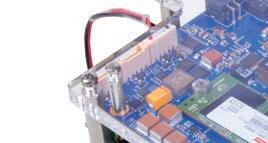
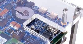
The 12009 COM Express Compact Type 6 Evaluation Board from Sealevel Systems, Inc. enables accelerated development of embedded computing prototypes, dramatically expedites electri cal hardware engineering, and reduces costs for NPI. Originally developed to control wearable, robotic exoskeleton systems, the board design quickly expanded in functionality while maintaining the mandated, extremely small footprint.
At 95 millimeters square, the 12009 Compact Evaluation Board is identical in size to a Compact Type 6 COM Express module. Designed to meet a wide variety of application needs, the 12009 evaluation board supplies a diverse I/O mix and robust process ing support. Standard I/O includes Gigabit Ethernet, USB 3.0, USB 2.0, GPIO, RS-232, and Mini DisplayPort. The carrier board is designed for the congatec® conga-TC370 COM Express family, with support for 8th generation Intel® Core™ processors, up to 64 GB DDR4 RAM, TPM 2.0 support, and consuming only 15W.
“We’ve pushed ourselves – and our products – to achieve extreme operating temperatures and to meet and exceed rigorous shock and vibration requirements for rugged applications. Adding on size constraints to optimize SWaP and achieve maximum functionally density makes for a rewarding challenge – once we achieve it,” says Jeff Baldwin, Director of Engineering for Sealevel.
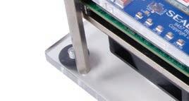
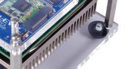
The complete evaluation kit (Part #12009-001-KT) includes a Type 6 module with i3-8145UE CPU and 8 GB DDR4 RAM. Additionally, to improve the devel opment process, the kit includes a 128GB M.2 SATA SSD module (supports Windows® and Linux® oper ating systems), desktop power supply, and a wide variety of cables to facilitate connections to serial and Ethernet ports and optional fans. Power button and feedback LED also included.
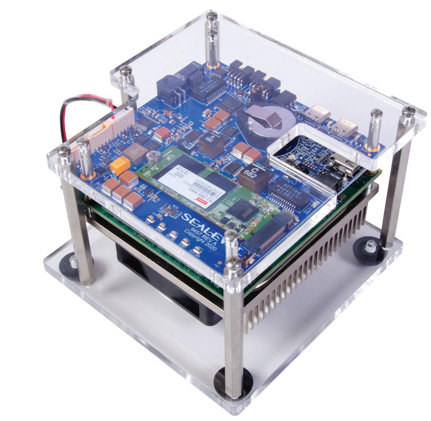
The 12009 COM Express Type 6 Evaluation Board features a wide operating temperature range of 0ºC to 70ºC and is powered via a locking, four-position Molex Micro-Fit connector.
FEATURES
Ą Designed for the congatec® conga-TC370 COM Express Family
Ą 0ºC to 70ºC Wide Operating Temperature Range
Ą (2) 10/100/1000 Gigabit Ethernet Headers
Ą (2) USB 3.0 Type-C Connectors
Ą (3) USB 2.0 Headers
Ą (4) GPIO Headers
Ą (1) RS-232 Header
Ą (1) UART Interface
Ą (1) Mini DisplayPort Connector
Ą (1) M.2 SATA SSD Interface
Embedded Computing Design
Development & Evaluation Kits https://www.sealevel.com/product/12009-001-KT/ Sealevel Systems, Inc. www.sealevel.com/ sales@sealevel.com 864-843-4343 @SealevelSystems www.linkedin.com/company/sealevel-systems-inc/ www.embeddedcomputing.com Embedded Computing Design RESOURCE GUIDE | Fall 2022 21
Embedded Computing
MSC C6B-ALP
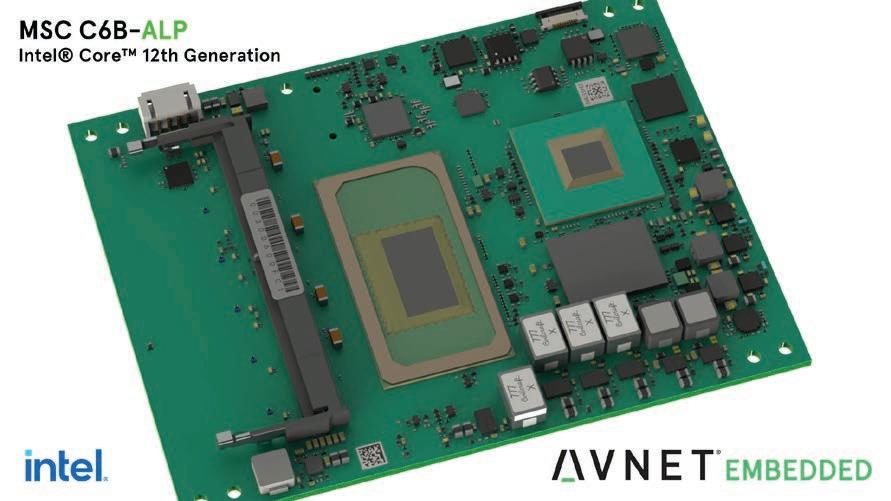
The MSC C6B-ALP COM Express module features the 12th Gen Intel® Core™ pro cessor, giving application designers a great variety of choices of power efficient and performant compute solutions. Offering a great scalability of performance, the module is ideal for compute-intense applications in medical, transportation, video surveillance and gaming. The new Intel® performance hybrid architecture combines Performance-cores and Efficient-cores with the Intel® Thread Director, providing intelligent workload optimization. The architecture scales up to 14 cores and 20 threads at 45/35W thermal design power (TDP).
For applications with a need for lower power dissipation, select processor vari ants can be operated down to 12W TDP. For highest data throughput the mod ule enables fast DDR5-4800 memory technology. Up to two SO-DIMMs can be installed for a total memory capacity from eight to 64GB. I/O located on COM Express carrier designs can be connected to the module via eight PCIe (mix of Gen 4/3) lanes and an eight lane PEG port capable of PCIe Gen 4. The Ethernet interface provides up to 2.5GbE bandwidth based on the Intel® i225 network controller. Sys tem investments are well protected through long-term availability of the module, designed and manufactured by Avnet Embedded.
Avnet Embedded www.avnet.com/embedded
FEATURES:
Ą 12th Gen Intel
Core
processors
Ą Up to 64GB DDR5-4800 SDRAM, dual channel
Ą Intel
Iris
Xe architecture Graphics, up to 96 EUs
Ą PCI Express® 4×1 lanes, configurable up to x4 (Gen 3) PCI Express® 1×4 (Gen 4)
Ą Four USB 3.1 Gen 1/2 and eight
product availability
customization available
2.0
AvnetEmbedded@avnet.com
www.linkedin.com/company/avnetembedded/ https://embedded.avnet.com/product/msc-c6b-alp/
Embedded
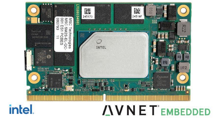
The MSC SM2S-EL module features Intel®’s next-generation low-power, multi-core system-on-chip (SOC) Atom generation (codenamed “Elkhart Lake”). Built on 10nm process technology, the SoC integrates the next-generation Intel® Atom processor core architecture and graphics accelerators, memory controller and rich I/O func tionality into a single package. The module is designed for extended temperature range and 24/7 operation, making it an ideal platform for mission-critical tasks that require a reliable and performant compute base. It provides significant per formance gains over previous Atom generations, allowing for technology upgrades within existing power and cooling requirements defined by the system design.
The new MSC SM2S-EL offers triple independent display support with a maximum of 4k resolution, DirectX 12, fast LPDDR4x memory with up to 16GB and optional IBECC capabilities, eMMC 5.1, USB 3.1 and PCIe Gen 3 on a power-saving and cost-efficient SMARC 2.1.1 Short Size module.
For evaluation and design-in of the MSC SM2S-EL module, Avnet Embedded pro vides a suitable SMARC 2.1.1 development platform. A complete, ready-to-run Starter kit is also available.
FEATURES:
SMARC 2.1 module family
Latest generation Intel® Atom, Pentium and Celeron processors
Up to 16GB LPDDR4x SDRAM with IBECC (only Atom SKUs)
Up to 256GB eMMC 5.1 Flash (optional)
Up to 4x PCI Express x1/x2/x4 Gen 3
customization options available
Designed for heavy industrial use
https://embedded.avnet.com/product/msc-sm2s-el/
Design
Embedded Hardware
®
™
®
®
USB
ports Ą Long-term
Ą Deep
MSC SM2S-EL
Hardware Avnet Embedded www.avnet.com AvnetEmbedded@avnet.com www.linkedin.com/company/avnetembedded/
Ą
Ą
Ą
Ą
Ą
Ą Deep
Ą
22 Embedded Computing Design RESOURCE GUIDE | Fall 2022 www.embeddedcomputing.com
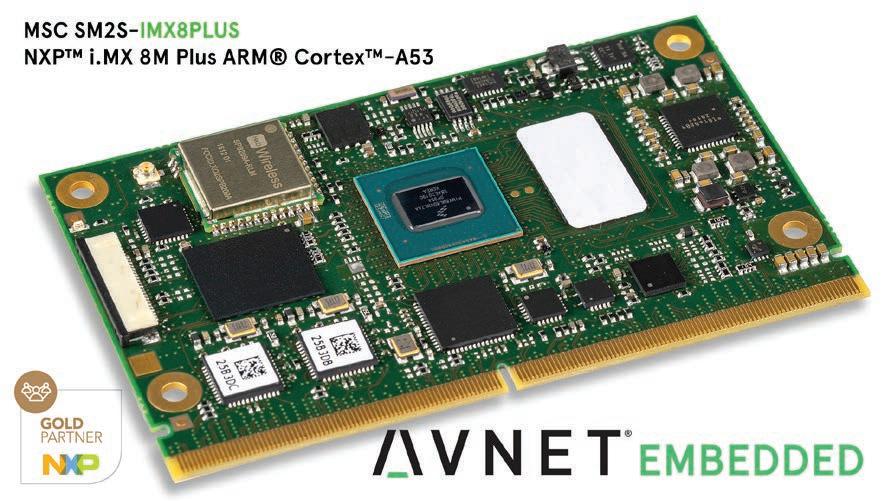
MSC SM2S-IMX8PLUS
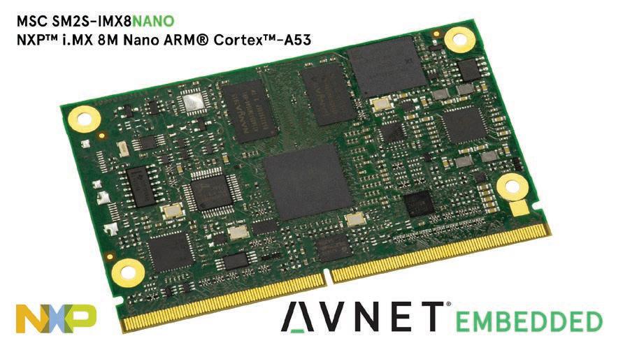
The MSC SM2S-IMX8PLUS module features NXP’s i.MX 8M Plus processors that are based on latest 14nm FinFET technology to allow high computing and graphics performance at very low power consumption combined with a high degree of functional integration. The MSC SM2S-IMX8PLUS offers dual- or quad-core ARM Cortex-A53 processors in combination with the ARM Cortex-M7 Real-Time Processor, a GC7000UL multimedia 2D/3D GPU and a Machine Learning Accelerator (2.3 TOPS). It provides fast LPDDR4 memory, up to 256GB eMMC Flash memory, 2x Gigabit Ethernet with IEEE 1588 support and one of them with TSN support, PCI Express Gen 3, USB 3.0, USB 2.0, an on-board Wireless Module (WLAN/BT), an Image Signal Processor supporting 2x MIPI-CSI (4-lane), as well as an extensive set of interfaces for embedded applications. The module is compliant with the new SMARC™ 2.1 standard, allowing easy integration with SMARC baseboards. For evaluation and design-in of the SM2S-IMX8PLUS module, Avnet Embedded provides a development platform and a starter kit. Support for Linux is available (Android support on request).
Avnet Embedded
www.avnet.com/embedded
FEATURES:
Ą SMARC 2.1 module family
Ą Dual or quad-core ARM Cortex-A53 Applications Processor up to 1.8GHz
Ą GC7000UL 2D/3D Graphics Processor with OpenCL and Vulkan support
Ą Machine Learning Accelerator (2.3 TOPS) (NPU not available on ”Plus Quad Lite“)
Ą PCI Express x1 Gen 3
Ą Industrial temperature range and 24/7 operation
Ą Deep customization available
https://embedded.avnet.com/product/msc-sm2s-imx8plus/
AvnetEmbedded@avnet.com
www.linkedin.com/company/avnetembedded/
MSC SM2S-IMX8NANO
The flexible MSC SM2S-IMX8NANO SMARC 2.1 module family is highly scal able and equipped with i.MX 8M Nano Application Processors, manufactured by NXP using 14nm FinFET process technology. The module integrates sin gle-, dual- and quad-core ARM Cortex-A53 processors up to 1.6GHz, an ARM Cortex-M7 Real-Time Processor and an efficient multimedia 2D/3D GPU. The thermal design power (TDP) ranges from 2W to 4W.
The MSC SM2S-IMX8NANO offers cost-effective DDR4 memory technology combined with up to 64GB eMMC Flash memory, and various interfaces for embedded applications such as Gigabit Ethernet, USB 2.0, dual-channel LVDS or MIPI-DSI and MIPI CSI-2 for connecting a camera are available. The module is compliant with the new SMARC 2.1 standard, allowing easy integration with SMARC baseboards. For evaluation and design-in of the SM2S-IMX8NANO module, Avnet Embedded provides a development platform and a starter kit. Support for Linux is available (Android support on request).
Ą
FEATURES:
Ą
SMARC 2.1 module family
Single, dual or quad-core ARM Cortex-A53 Applications Processor up to 1.5GHz
ARM Cortex-M7 Real-Time Processor up to 750MHz
Up to 2GB DDR4 SDRAM at 2400MT/s
Dual-channel LVDS/MIPI-DSI x4 (optional)
Long-term product availability
Deep customization available
Embedded Computing Design
Embedded Hardware
Embedded Hardware Avnet Embedded www.avnet.com/embedded AvnetEmbedded@avnet.com www.linkedin.com/company/avnetembedded/ https://embedded.avnet.com/product/msc-sm2s-imx8nano/
Ą
Ą
Ą
Ą
Ą
www.embeddedcomputing.com Embedded Computing Design RESOURCE GUIDE | Fall 2022 23
MSC OSM-MF-IMX8NANO
The MSC OSM-MF-IMX8NANO is based on the new OSM 1.1 standard (Size-M) “Medium”, which defines low-cost embed ded computer modules that are completely machine proces sible during soldering, assembly and testing.
Highly scalable and equipped with i.MX 8M Nano Applica tion Processors, manufactured by NXP using 14nm FinFET process technology, the module integrates single-, dual- and quad-core ARM Cortex-A53 processors up to 1.5GHz, an ARM Cortex-M7 Real-Time Processor and an efficient mul timedia 2D/3D GPU. The thermal design power (TDP) ranges from 2W to 4W.
The MSC OSM-MF-IMX8NANO provides fast and low-power LPDDR4 memory technology, combined with up to 256GB eMMC Flash memory. Various interfaces for embedded appli cations such as Gigabit Ethernet (RGMII), USB 2.0, MIPI-DSI and MIPI CSI-2 (4-lane) for connecting a camera are available.
For evaluation and design-in of the new OSM-MF-IMX8NANO module, Avnet Embedded provides a development platform and a Starter Kit. A Yocto-based Linux Board Support Package is available (Android support on request).
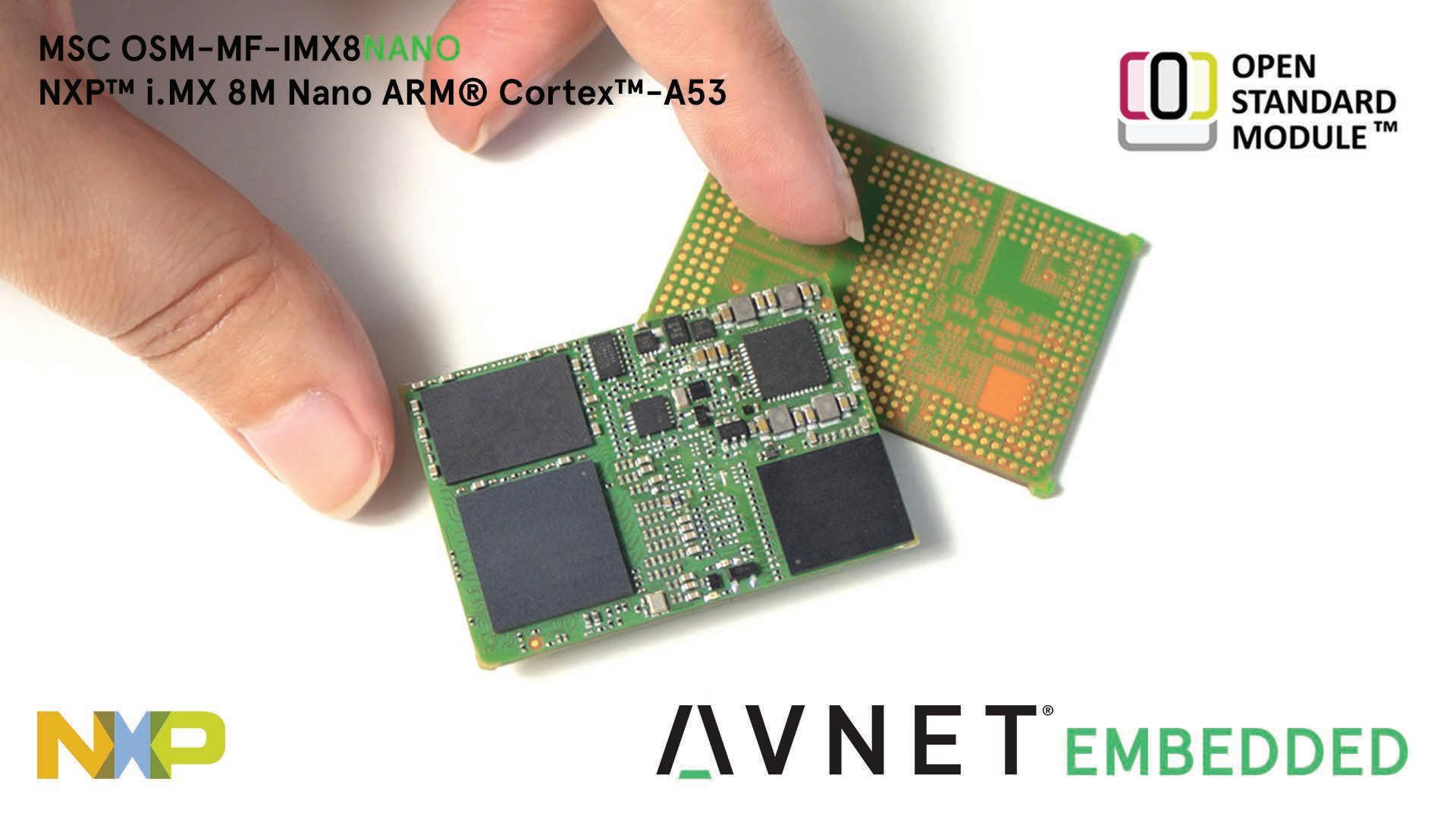
FEATURES
Ą New OSM design standard
Ą Single, dual or quad-core ARM Cortex-A53 Applications Processor up to 1.5GHz
Ą ARM Cortex-M7 Real-Time Processor up to 750MHz
Ą Vivante multimedia 2D/3D Graphics Processor
Ą Up to 256GB eMMC Flash
Ą Up to 1GB LPDDR4 SDRAM
Ą OSM-MF compliant, 476 Pin, RM 1.25 mm
Ą Extremely compact, versatile design
Ą Deep customization options
Ą Long-term product support
https://embedded.avnet.com/product/msc-osm-mf-imx8nano/
Embedded Computing Design
Embedded Hardware
Avnet Embedded www.avnet.com/embedded AvnetEmbedded@avnet.com www.linkedin.com/company/avnetembedded/ 24 Embedded Computing Design RESOURCE GUIDE | Fall 2022 www.embeddedcomputing.com
MSC HSD-ILDL
The MSC HSD-ILDL COM-HPC Server module hosts the Intel® Xeon® D-1700 pro cessor and delivers server-class performance on an embedded form factor. The processor is a fully integrated System on Chip (SoC) combining up to ten Xeon cores, memory controller, high-bandwidth network and multiple PCIe root com plexes on a single socket.
The on-chip network controller facilitates up to eight Ethernet ports with differ ent configuration options ranging from 1G to 25G per port and an aggregated throughput of up to 100G. An additional Ethernet port based on Intel® i225 pro vides 1GbE/2.5GbE bandwidth and TSN capability for real-time applications. An extensive set of PCI Express lanes with Gen 4 and Gen 3 support allow for connect ing external HW accelerators, FPGAs, storage and I/O devices.
Select variants of the MSC HSD-ILDL can be operated at extended temperature range with true 24/7 utilization. This supports system designs exposed to harsh environmental conditions that require a reliable compute engine.
System investments are well protected through long-term availability of the mod ule. In addition, the COM-HPC standard enables performance scaling and migrat ing applications to future technology upgrades when they become available.
Avnet Embedded
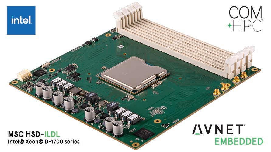
www.avnet.com/embedded
FEATURES:
Ą COM-HPC Server module
Ą
Ideal for IoT, AI/deep learning, edge computing, HPC, workload consolidation
Ą Intel® Xeon® D-1700 processor
Ą Server-class multi-core system on chip (SoC)
Ą Up to 10 cores
Ą Industrial temperature range and 24/7 operation
Ą Long-term product availability
https://embedded.avnet.com/product/msc-hsd-ildl/
AvnetEmbedded@avnet.com
www.linkedin.com/company/avnetembedded/
TS-4900
The TS-4900 is a high-performance TS-SOCKET System on Module based on the NXP i.MX6 CPU which implements the Arm® Cortex®-A9 architec ture clocked at 1 GHz (Single or Quad Core) and paired with 1GB or 2GB of DDR3 RAM.
Several industry-standard interfaces and connections such as Gigabit Ethernet, WiFi and Bluetooth, USB, SATA II, PCI Express, and more make the TS-4900 a great fit for nearly any embedded systems application, especially those needing wireless connections like industrial internet of things (IIOT) gateway.
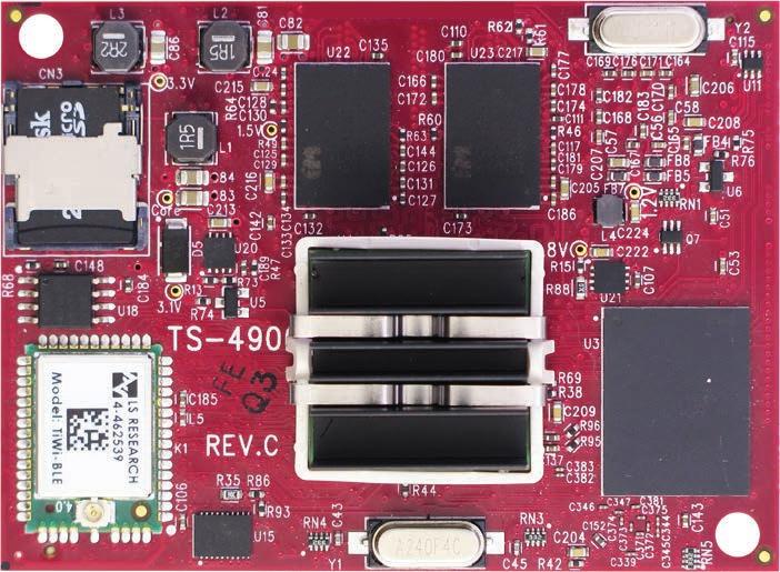
www.embeddedTS.com
sales@embeddedTS.com

embeddedTS
480-837-5200
Embedded Computing Design
Embedded Hardware: PICMG COM-HPC
Embedded Hardware embeddedTS
@
https://www.embeddedts.com/products/TS-7900
FEATURES Ą 1 GHz Single or Quad Core Cortex-A9 Arm CPU Ą 2 GB DDR3 RAM Ą 4GB MLC eMMC flash storage Ą Up to 70x DIO, 2x I2C, 1x I2S, 2x SPI, 2x CAN Ą Industrial temperature range (-40°C to 85°C) www.embeddedcomputing.com Embedded Computing Design RESOURCE GUIDE | Fall 2022 25
The new conga-HPC/uATX industrial-grade COM-HPC carrier board in Micro-ATX form factor is designed for embedded longterm availability of at least seven years, which eliminates the design risks, revision requirements and supply chain uncertain ties of standard or semi-industrial-grade motherboards that are usually only deliverable for three to five years. As it is processor socket and vendor independent, the board can be equipped with any high-end Computer-on-Module available in COM-HPC Client Size A, B or C, making OEM designs even more flexible and sus tainable. Impressive scalability across the entire range of 12th Generation Intel Core processor-based COM-HPC modules. Per formance options for the new conga-HPC/uATX carrier board range from the conga-HPC/cALS COM-HPC Client Size C mod ules, offering the currently highest embedded client performance with 16-core Intel Core i9 processor, to the masters of price/ performance optimization – the conga-HPC/cALP COM-HPC Client Size A modules with Intel Celeron 7305E processor.
The combination of application-ready industrial-grade COMs & carrier boards with tailored cooling solutions and comprehensive BSPs for all leading RTOSes and the real-time hypervisor from Real-Time Systems is perfect for fastest time-to-market, pro duces lowest non-recurring engineering costs, enables custom ers to react very quickly to changing market requirements and reduces the effort to scale the performance of Micro-ATX based systems to a minimum. It allows customers to create a full prod uct portfolio based on one single carrier concept.
The carrier board offers the latest interface enhancements such as PCIe Gen4 and USB 4 and is a perfect fit for system designs with congatec’s latest high-end COM-HPC Client modules based on the 12th generation Intel Core i9/7/5/3 desktop processors (formerly code-named Alder Lake-S). Most impressive is the fact that engineers can now leverage Intel’s innovative performance hybrid architecture. Offering of up to 16 cores/24 threads, 12th Gen Intel Core processors provide a quantum leap in multitasking and scalability levels.
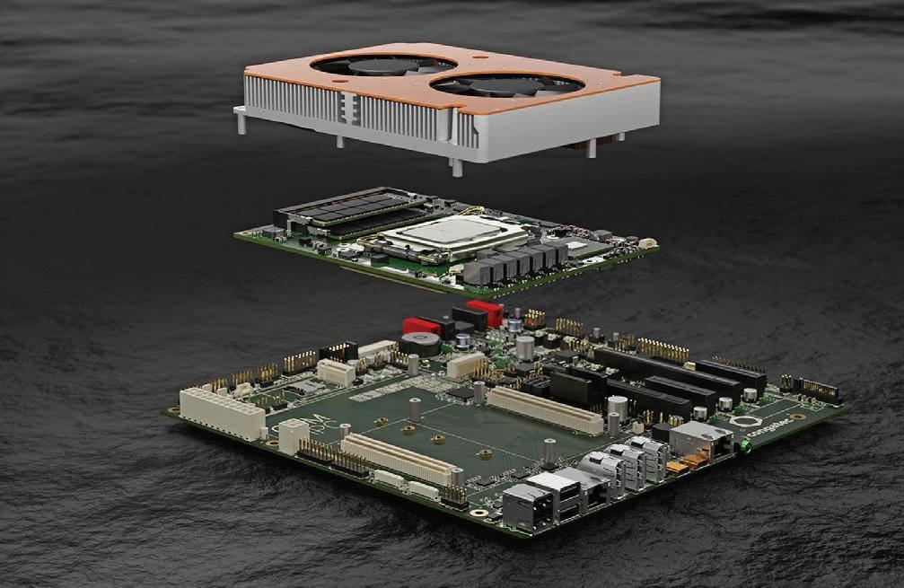
Next-gen IoT and edge applications benefit from up to 8 opti mized Performance-cores (P-cores) plus up to 8 low power Efficient-cores (E-cores) and DDR5 memory support to accelerate multithreaded applications and execute background tasks more
efficiently. Optimized for highest embedded client performance, the graphics of the LGA processor based modules delivers now up to 94% faster performance and its image classification inference per formance has nearly tripled with up to 181% higher throughput. In addition, the modules offer massive bandwidth to connect discrete GPUs for maximum graphics and GPGPU based AI performance.
FEATURES
Ą Application Carrier Board for COM-HPC Client Type Modules (Sizes A, B, C) in Micro-ATX form factor. Size 244 x 244 mm2
Ą Besides highest bandwidth and performance, the new flagship COM-HPC Client modules impress with dedicated AI engines supporting Windows ML, Intel Distribution of OpenVINO toolkit and Chrome Cross ML
Ą
Different AI workloads can seamlessly be delegated to the P-cores, E-cores, as well as the GPU execution units to process even the most intensive edge AI workloads
Ą The built-in Intel Deep Learning boost technology leverages different cores via Vector Neural Network Instructions (VNNI), and the integrated graphics supports AI accelerated DP4a GPU instructions that can even be scaled to dedicated GPUs
Ą Intel’s lowest power built-in AI accelerator, the Intel Gaussian & Neural Accelerator 3.0 (Intel GNA 3.0), enables dynamic noise suppression and speech recognition and can even run while the processor is in low power states for wake-up voice commands.
858-457-2600
Micro-ATX carrier board eco-system for COM-HPC
Embedded Computing Design
Embedded Hardware www.congatec.com congatec www.congatec.com sales-us@congatec.com
www.linkedin.com/company/congatec/ @ congatecAG
26 Embedded Computing Design RESOURCE GUIDE | Fall 2022 www.embeddedcomputing.com
TS-7800-V2
Powered by the Marvell Armada 385 Dual Core 1.3 GHz Arm® Cortex® A9-based CPU, the embeddedTS TS-7800-V2 industrial Single Board Computer (SBC) stands out from the crowd with its high-performance components, connectivity options, and an unbelievable feature set pack aged into a small footprint in both size and power. It's a general-purpose, low-power SBC ready to tackle demanding applications, including data acquisition, IoT, industrial automation, or any rugged deployment.
The guaranteed 10+ year lifecycle ensures a long-term deployment in the field, free from expensive replacements that come from short, dis posable lifecycles, which are all too common. With the included heat sink, the fanless design of the TS-7800-V2 can withstand high vibra tion, and even with two CPU cores running at 1GHz and tasked to their max, the system can operate at a wide temperature range of -40 °C to 85 °C.
FEATURES
Marvell Armada 385 Dual Core 1.3 GHz Arm-based CPU
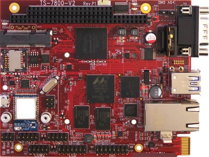
1 DDR3 RAM
4 GB MLC eMMC Flash
Flexible Data Storage: eMMC, SATA, mSATA, SD Card or uSD Card Expansion
Easily Interfaces via PC/104, USB 3.0, Gigabit Ethernet, ADC, GPIO and More
Hardware
TS-7100-Z
embeddedTS is proud to introduce the TS-7100-Z, our smallest single board computer in an optional DIN-mountable enclosure that measures 2.4" by 3.6" by 1.7", powered by the Arm® Cortex®-A7 based iMX6 Ultra Lite CPU. It ships with industry-standard interfaces, including Ethernet, USB, RS-232, RS-485, and CAN.
For wireless connectivity, the TS-7100-Z comes with WiFi and Bluetooth module, as well as a NimbeLink/Digi cellular modem and mesh network socket. With all of these features packed into a smaller footprint, not only will the TS-7100-Z fit in your cabinet, but it can also help to replace other peripherals and modules to free up even more space and get more done. Combining all of these components into one small DIN-mounted unit, we provide the ability to promote hot swapping in the field, limiting costly technician time and troubleshooting.
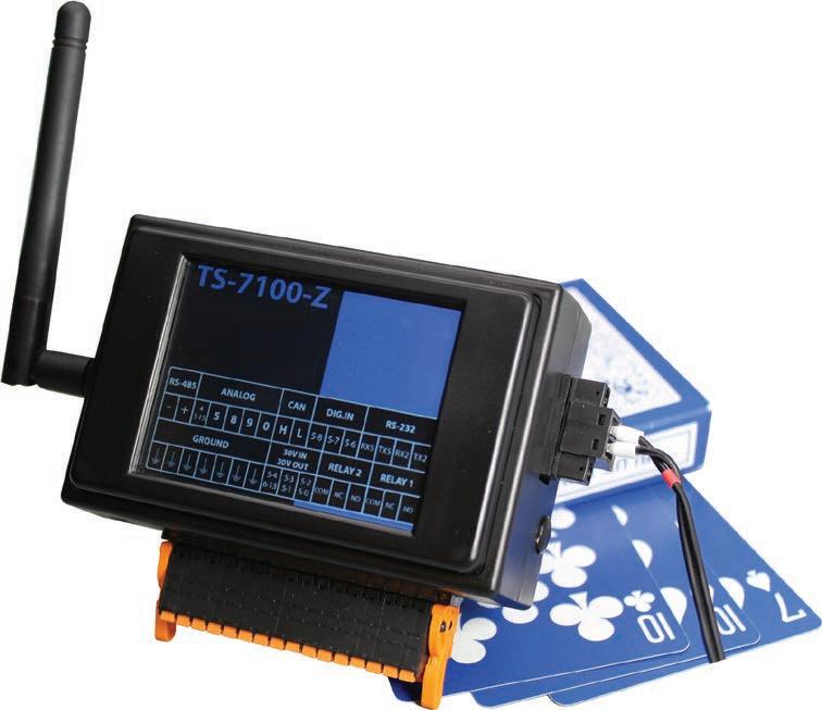
www.embeddedTS.com
Touchscreen
https://www.embeddedts.com/products/ts-7100-Z
sales@embeddedTS.com


embeddedTS
480-837-5200
Embedded Computing Design Embedded
embeddedTS
@
FEATURES Ą NXP i.MX 6UltraLite 696 MHz Arm® Cortex®-A7 Ą 512 MB RAM Ą 4 GB eMMC Flash Storage Ą 2 KB FRAM Storage Ą 3" 18-bit, 320x240, 135dpi Resistive
Display (Optional) Embedded Hardware embeddedTS www.embeddedTS.com sales@embeddedTS.com 480-837-5200 @ embeddedTS https://www.embeddedts.com/products/TS-7800-V2
Ą
Ą
Ą
Ą
Ą
www.embeddedcomputing.com Embedded Computing Design RESOURCE GUIDE | Fall 2022 27
K3841-Q μATX
The Industrial Motherboard K3841-Q μATX is equipped with the highly performant Intel® Q670E Chipset. It also offers a multitude of supporting processors such as the Intel® Core™ i9/i7/i5/i3(12th Gen) and the Intel® Pentium®/Intel® Celeron® processor series.
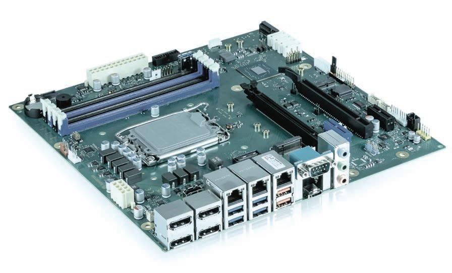
Designed and approved for 24/7 continuous operation and an enhanced temperature range up to 60 Celsius the K3841-Q μATX provides high functionality and fits perfect with special requirements of certain markets.
It offers basic manageability based on selected Intel® vPro® Essentials features. Besides, K3841-Q provides TSN and Realtime support (TCC) for specific industrial applications.
FEATURES:
Ą Intel® Q670E Chipset and Intel® 12th Gen Core™ i3/i5/i7/i9 Processors
Ą Latest DDR5 memory technology for best-in-class system performance
Ą Intel® UHD Graphics 7xx driven by Xe Architecture; 4x DisplayPort V1.4a @4k
Ą Strict lifecycle management and reliable product maintenance
https://www.kontron.com/en/products/k3841-q-uatx/p172727
Kontron
www.us.kontron.com

sales@us.kontron.com
888-294-4558
www.linkedin.com/company/kontron-north-america
Embedded Software, OSs, & Tools
TRACE32 Multi Core Debugger for TriCore Aurix
Lauterbach TriCore debug support at a glance: For more than 15 years Lauterbach has been supporting the latest TriCore microcontrollers. Our tool chain offers:
• Single and multi core debugging for up to 6 TriCore cores
• Debugging of all auxiliary controllers such as GTM, SCR, HSM and PCP
• Multi core tracing via MCDS on-chip trace or via high-speed serial AGBT interface
The Lauterbach Debugger for TriCore provides high-speed access to the target application via the JTAG or DAP protocol. Debug features range from simple Step/Go/Break up to AutoSAR OS-aware debugging. High speed flash programming performance of up to 340kB/sec on TriCore devices and intuitive access to all peripheral modules are included.
Lauterbach’s TRACE32 debugger allows concurrent debugging of all TriCore cores.


• Cores can be started and stopped synchronously.
• The state of all cores can be displayed side by side.
• All cores can be controlled by a single script.
Lauterbach, Inc. www.lauterbach.com
FEATURES
Ą Debugging of all auxiliary controllers: PCP, GTM, HSM and SCR
Ą Debug Access via JTAG and DAP
Ą AGBT High-speed serial trace for Emulation Devices
Ą On-chip trace for Emulation Devices
Ą Debug and trace through Reset
Ą Multicore debugging and tracing
Ą Cache analysis
info_us@lauterbach.com
508-303-6812
www.lauterbach.com/bdmtc.html
Embedded Computing Design
Embedded Hardware
28 Embedded Computing Design RESOURCE GUIDE | Fall 2022 www.embeddedcomputing.com
Lauterbach Debugger for RH850
Lauterbach RH850 debug support at a glance:
The Lauterbach Debugger for RH850 provides high-speed access to the tar get processor via the JTAG/LPD4/LPD1 interface. Debugging features range from simple Step/Go/Break to multi core debugging. Customers value the performance of high-speed flash programming and intuitive access to all of the peripheral modules.
TRACE32 allows concurrent debugging of all RH850 cores.
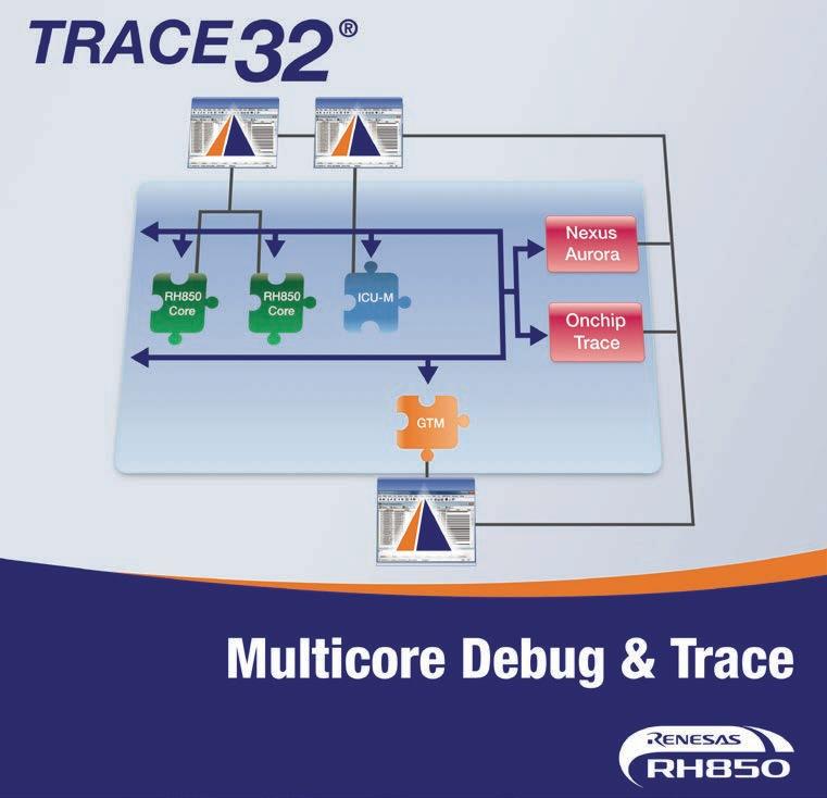
• The cores can be started and stopped synchronously.
• The state of all cores can be displayed side by side.
• All cores can be controlled by a single script.
All RH850 emulation devices include a Nexus trace module, which enables multi core tracing of program flow and data transactions. Depending on the device, trace data is routed to one of the following destinations:
• An on-chip trace buffer (typically 32KB)
• An off-chip parallel Nexus port for program flow and data tracing
• A high bandwidth off-chip Aurora Nexus port for extensive data tracing
The off-chip trace solutions can store up to 4GB of trace data and also provide the ability to stream the data to the host for long-term tracing, thus enabling effortless performance profiling and qualification (e.g. code coverage).
Lauterbach, Inc.
www.lauterbach.com
FEATURES
Ą AMP and SMP debugging for RH850, GTM and ICU-M cores
Ą Multicore tracing
Ą On-chip and off-chip trace support
Ą Statistical performance analysis
Ą Non intrusive trace based performance analysis
Ą Full support for all on-chip breakpoints and trigger features
Ą AUTOSAR debugging
info_us@lauterbach.com
508-303-6812 www.lauterbach.com/bdmrh850.html
SECO SMARC COMs: low power, low costs, many options
Leveraging multi-decade excellence in design and manufacturing, SECO embedded products feature leading edge processing technologies, based on x86, Arm, and FPGA architectures from world-class silicon vendors. SECO offers multiple standard form-factor computing platforms in addition to HMIs, fanless PCs, commu nication gateways, and custom product.
SECO’s SMARC product family offers multiple processor options within a compact Computer-On-Module standard for products that require high performance and low power usage. Providing a processor, memory, storage, display and Ethernet interfaces, USB, and more in a small footprint, SMARC offers an embedded computing module within a compact 3.23x1.97-inch standard form-factor.
SECO’s SMARC product family offers ARM, x86, and FPGA options, with associated Linux, Android, and Windows operating systems.

With client electronic design limited to an application-specific carrier board, SMARC modules merge the ability to withstand rugged environmental conditions with excellent scalability and high configurability. SMARC is the perfect fit for products ranging from industrial IoT to HMI and smart digital signage, to smart city and home automation.
Beyond SMARC modules, SECO wide portfolio of embedded boards also includes many other form factors, including Qseven®, COM Express®, COM-HPC®, and single board computer (SBC).
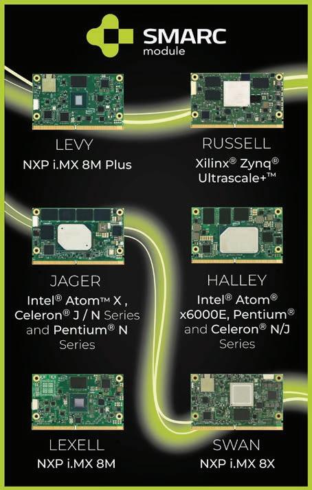
SECO www.seco.com
sales.us@seco.com
Ą
FEATURES:
Standard form-factor computing engines
Ą Design investment limited to the carrier board
Ą Scalable and future-proof solutions
Ą Long-term availability
Ą ARM and x86 processors
Ą Industrial temperature, conformal coat options
Ą Reduced time-to-market
https://edge.seco.com
+1-240-558-2014
www.linkedin.com/company/seco-spa/
Embedded Computing Design
Embedded Hardware
Embedded Software, OSs, & Tools
www.embeddedcomputing.com Embedded Computing Design RESOURCE GUIDE | Fall 2022 29
XEM8320: Xilinx Artix UltraScale+ Development Platform
The XEM8320 is the official development platform for the latest addi tion to the Xilinx 16nm UltraScale+ FPGA family. Supporting the new Artix UltraScale+ for rapid application development, the XEM8320 includes the FrontPanel SDK, Opal Kelly’s flag ship software/gateware environment for high-performance USB 3.0 Super Speed interfacing, as well as multiple SYZYGY ports for modular peripheral expansion.
Part of Xilinx’s cost-optimized portfo lio, the Artix UltraScale+ (AUP) is built on the same mature 16nm technol ogy that underpins Kintex and Zynq devices in the family. The AUP offers PCIe Gen 3 and serial I/O peripheral support with gigabit transceivers up to 16.375 Gbps for high-throughput sensor data, DSP computa tion, and network bandwidth. Applications include ultra high-end data acquisition, data and video analytics, and localized artificial intelligence and machine learning.
Opal Kelly’s FrontPanel SDK enables rapid development of highperformance software-connected FPGA applications for prototypes, proof-of-concept, and production. FrontPanel’s flexible architec ture and proprietary firmware allows developers to focus on their core expertise without consuming precious FPGA resources. The XEM8320 and FrontPanel provide a powerful research, develop ment, and prototyping platform for next generation applications.
A new generation of FPGA peripherals is supported with four SYZYGY Standard and two SYZYGY transceiver ports. Higher per formance than Digilent’s prolific PMOD standard and less ”greedy“ than high-pin count FMC (VITA 57.1) peripherals, SYZYGY offers a modern compromise with features such as SmartVIO for I/O volt ages compatible with today's semiconductor devices and FPGA I/O architectures. Designed for single-device peripherals, SYZYGY shares the PMOD approach of supporting multiple, smaller periph erals than FMC. As a result, system integrators can piece multiple devices together into a single system.
For low- to mid-volume product development, the company offers a path to production with the XEM8310 system-on-module (SOM).
Built with the same Artix UltraScale+ FPGA as the XEM8310, the compact module is perfect for production deployments in researchgrade test and measurement, data acquisition, instrumentation, and more. Lifecycle-managed, supported by an ISO 9001 quality management system, and step pricing strategy for quantity dis counts, Opal Kelly's modular solutions are perfect for OEMs and mid-market solution providers.
FEATURES
Ą Xilinx Artix UltraScale+ AUP25 FPGA with 16nm technology
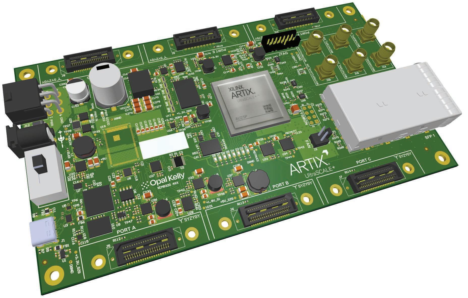
Opal Kelly’s FrontPanel SDK for USB 3.0

Single-input power system (+8V to +14V)
1 GiB DDR4
GTH Transceivers up to 16.375 Gbps
Programmable clock generator
4x SYZYGY Standard Ports (learn more at https://syzygyfpga.io)
2x SYZYGY Transceiver Ports
2x SFP+ cages
6x SMA for transceiver access
FrontPanel SDK platforms: Windows, Linux, macOS
Embedded Computing Design
Ą
Ą
Ą
Ą
Ą
Ą
Ą
Ą
Ą
Ą
Embedded Hardware https://opalkelly.com/products/xem8320/ Opal Kelly Incorporated www.opalkelly.com sales@opalkelly.com 217-391-3724 www.linkedin.com/company/opal-kelly-incorporated twitter.com/opalkelly
30 Embedded Computing Design RESOURCE GUIDE | Fall 2022 www.embeddedcomputing.com
TRACE32 JTAG/ETM Debugger for ARMv8
Lauterbach ARMv8 support at a glance:
More than 17 years of experience in ARM debugging enable Lauterbach to provide best-in-class debug and trace tools for ARMv8 based systems:
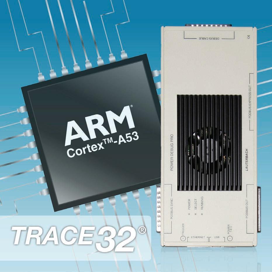
• Multicore debugging and tracing for any mix of ARM and DSP cores
• Support for all CoreSight components to debug and trace an entire SoC
• Powerful code coverage and run-time analysis of functions and tasks
• OS-aware debugging of kernel, libraries, tasks of all commonly used OSs
Lauterbach debug tools for ARMv8 help developers through out the whole development process, from the early pre-silicon phase by debugging on an instruction set simulator or a virtual prototype over board bring-up to quality and maintenance work on the final product.
Debugger features range from simple step/go/break, program ming of on-chip-flash, external NAND, eMMC, parallel and serial NOR flash devices, support for NEON and VFP units, to OS-aware debug and trace concepts for 32-bit and 64-bit multicore systems.
TRACE32 debuggers support simultaneous debugging and tracing of homogeneous multicore and multiprocessors sys tems with one debug tool.
Start/Stop synchronization of all cores and a time-correlated display of code execution and data r/w information provides the developer with a global view of the system's state and the interplay of the cores.
Ą
FEATURES
Ą
Full support for all CoreSight components
Full architectural debug support
Ą Support for 64-bit instruction set and 32-bit instruction sets ARM and THUMB
Ą
32-bit and 64-bit peripherals displayed on logical level
Ą Support for 32-bit and 64-bit MMU formats
Ą Auto-adaption of all display windows to AArch32/ AArch64 mode
Ą Ready-to-run FLASH programming scripts
Ą Multicore debugging
Ą
On-chip trace support (ETB, ETF, ETR)
Ą Off-chip trace tools (ETMv4)
Ą
AMP debugging with DSPs, GPUs and other accelerator cores
Embedded Computing Design
Lauterbach, Inc. www.lauterbach.com info_us@lauterbach.com 508-303-6812 www.lauterbach.com/bdmarmv8a.html Embedded Processing: Arm About our Products • Everything from a single source • Open system • Open user interface for everything • Long-term investment through modularity and compatibility • The full array of architectures supported Our Company Philosophy • High-tech company with long-term experience • Technical know-how at the highest level • Worldwide presence • Time to market www.embeddedcomputing.com Embedded Computing Design RESOURCE GUIDE | Fall 2022 31
Apacer supplies customers with high performance, reliable, high value NAND flash memory and DRAM memory modules, which are widely applied in a range of applications including embed ded, IPC, transportation, military, gaming, healthcare, and IOT. Together with its broad R&D, design, manufacturing, and mar keting strengths, it has become a leading global manufacturer in the industry.

Apacer industrial SSD solutions include NVMe/PCIe, SATA, PATA, Card, and USB interfaces. Form factors cover 2.5”, 1.8”, M.2, MO-300, MO-300B, MO-297, MO-276, 7-Pin Module, CF, CFast, CFexpress, SD, microSD, USB Flash Drive, and USB Flash module. Apacer understands how important the steadiness and conve nience of digital data storage and sharing are for users in this era of big data. Apacer has dedicated itself to pursuing excel lence and elevating the energy for development. We guarantee the use of high-end die components, and design and manufac ture our products with innovation and craftsmanship to provide the digital storage solution closest to the market and customers’ requirements.
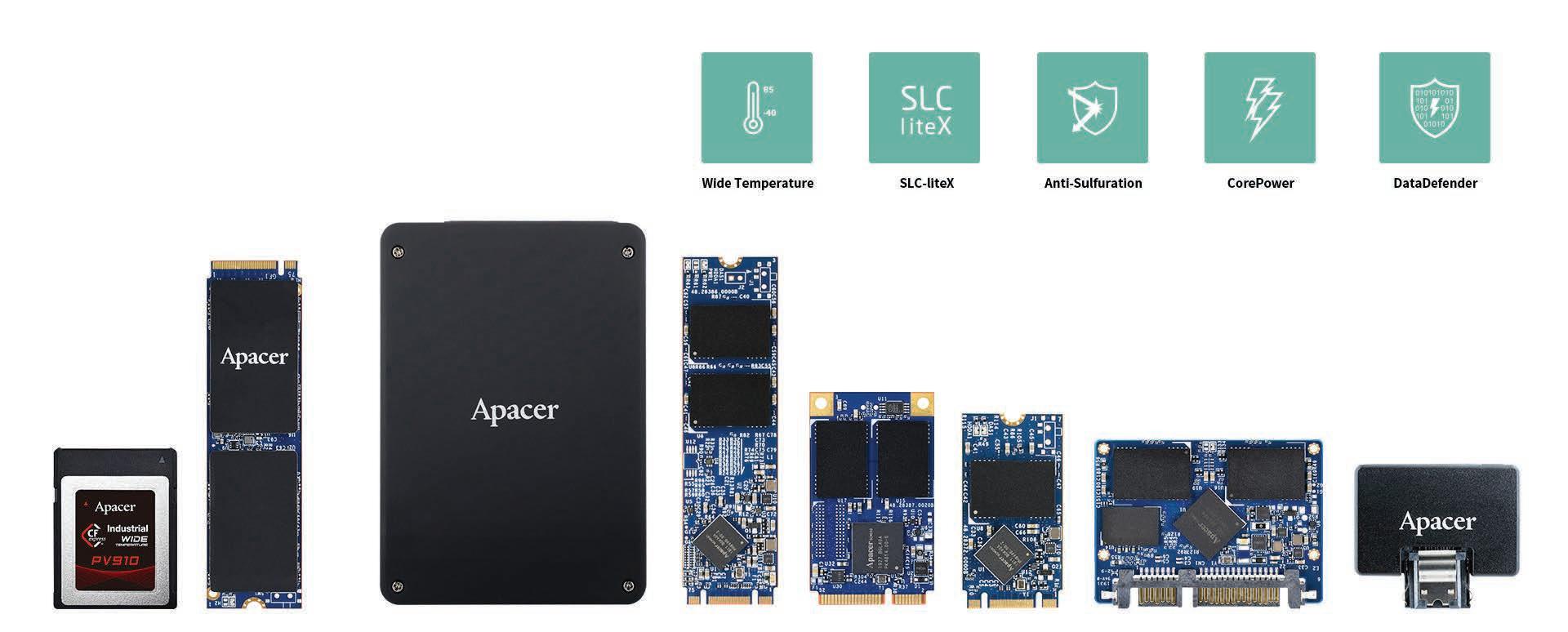
FEATURES
Ą Anti-Sulfuration, the world’s first patented anti-sulfuration memory modules and anti-sulfuration SSDs with the industry’s highest level of anti-corrosion certification can meet the needs of industrial products facing harsh environments.
Ą CorePower, a hardware-based technology designed to prevent data loss and ensure the stability of data transmission during a power outage by implementing backup power supply that allows sufficient time to move all cached data to NAND flash.
Ą DataDefender™, combines both firmware and hardware mechanisms to ensure data integrity. Together, they allow more time for volatile data to be stored in the event of power loss.
Ą SLC-liteX, Apacer’s 3D NAND SLC-liteX technology breaks through the limitations of existing technology and provides high P/E cycles.
Ą Wide Temperature, Apacer’s products are designed with wide temperature support to ensure operation reliability in extreme temperatures ranging from -40° C to 85° C. Apacer’s wide-temp series of products, including memory chips, passive elements, and PCB, are all full-scale industrial grade. These products have passed industrial extended temperature tests and the most extreme thermal cycling test, ensuring their quality, reliability, and durability.
Embedded Computing Design
Industrial SSD Memory & Storage https://industrial.apacer.com/en-ww Apacer Memory America Inc. www.apacer.com ssdsales@apacerus.com 408-518-8699 32 Embedded Computing Design RESOURCE GUIDE | Fall 2022 www.embeddedcomputing.com
Ą
PCAN-PC/104
FEATURES:
Ą Form factor PC/104
Ą Multiple PC/104 cards can be operated in parallel (interrupt sharing)
Ą 14 port and 8 interrupt addresses are available for configuration using jumpers
Ą 1 or 2 High-speed CAN channels (ISO 11898-2)
Ą Bit rates from 5 kbit/s up to 1 Mbit/s
Ą Compliant with CAN specifications 2.0A (11-bit ID) and 2.0B (29-bit ID)
Ą Connection to CAN bus through D-Sub slot bracket, 9-pin (in accordance with CiA® 303-1)
Ą NXP SJA1000 CAN controller, 16 MHz clock frequency
Ą NXP PCA82C251 CAN transceiver
Ą 5-Volt supply to the CAN connection can be connected through a solder jumper, e.g., for external bus converter
Ą Optionally available with galvanic isolation on the CAN connection up to 500 V, separate for each CAN channel
Ą Extended operating temperature range from -40 to 85 °C (-40 to 185 °F)
PEAK-System Technik GmbH
www.peak-system.com/quick/PC104-1
CAN Interface for PC/104
The PCAN-PC/104 card enables the connection of one or two CAN networks to a PC/104 system. Multiple PCAN-PC/104 cards can easily be operated using interrupt sharing.

The card is available as a single or dual-channel version. The opto-decoupled versions also guarantee galvanic isolation of up to 500 Volts between the PC and the CAN sides.
The package is also supplied with the CAN monitor PCAN-View for Windows and the programming interface PCAN-Basic.
info@peak-system.com
www.linkedin.com/company/peak-system
+49 (0) 6151-8173-20
@PEAK_System
Ą
PCAN-PC/104-
FEATURES:
Ą Form factor PC/104
Ą Use of the 120-pin connection for the PCI bus
Ą Up to four cards can be used in one system
Ą 1 or 2 High-speed CAN channels (ISO 11898-2)
Ą Bit rates from 5 kbit/s up to 1 Mbit/s
Ą Compliant with CAN specifications 2.0A (11-bit ID) and 2.0B (29-bit ID)
Ą Connection to CAN bus through D-Sub slot bracket, 9-pin (in accordance with CiA® 303-1)
Ą NXP SJA1000 CAN controller, 16 MHz clock frequency
Ą NXP PCA82C251 CAN transceiver
5-Volt supply to the CAN connection can be connected through a solder jumper, e.g., for external bus converter
Extended operating temperature range from -40 to 85 °C (-40 to 185 °F)
Ą Optionally available with galvanic isolation on the CAN connection up to 500 V, separate for each CAN channel
Ą PC/104-ISA stack-through connector
Technik
CAN Interface for PC/104-Plus
The PCAN-PC/104-Plus card enables the connection of one or two CAN networks to a PC/104-Plus system. Up to four cards can be operated, with each piggy-backing off the next. The CAN bus is connected using a 9-pin D-Sub plug on the slot bracket supplied.
The card is available as a single or dual-channel version. The opto-decoupled versions also guarantee galvanic isolation of up to 500 Volts between the PC and the CAN sides.
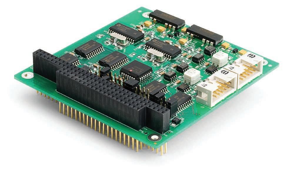
The package is also supplied with the CAN monitor PCAN-View for Windows and the programming interface PCAN-Basic.
info@peak-system.com


www.linkedin.com/company/peak-system
+49 (0) 6151-8173-20
Embedded Computing Design
Plus Industrial PEAK-System
GmbH www.peak-system.com/quick/PC104-2
@PEAK_System
Industrial
www.embeddedcomputing.com Embedded Computing Design RESOURCE GUIDE | Fall 2022 33
Ą
Ą
PCAN-PC/104-Plus Quad
FEATURES:
Form factor PC/104
Ą Use of the 120-pin connection for the PCI bus
Ą Up to four cards can be used in one system
Ą 4 High-speed CAN channels (ISO 11898-2)
Ą Bit rates from 5 kbit/s up to 1 Mbit/s
Ą Compliant with CAN specifications 2.0A (11-bit ID) and 2.0B (29-bit ID)
Ą Connection to CAN bus through D-Sub slot brackets, 9-pin (in accordance with CiA® 303-1)
Ą FPGA implementation of the CAN controller (SJA1000 compatible)
Ą NXP PCA82C251 CAN transceiver
Ą Galvanic isolation on the CAN connection up to 500 V, separate for each CAN channel
Ą 5-Volt supply to the CAN connection can be connected through a solder jumper, e.g., for external bus converter
Ą Extended operating temperature range from -40 to 85 °C (-40 to 185 °F)
Ą Optionally available: PC/104-ISA stack-through connector
PEAK-System Technik GmbH
www.peak-system.com/quick/PC104-3
Four-Channel CAN Interface for PC/104-Plus
The PCAN-PC/104-Plus Quad card enables the connection of four CAN networks to a PC/104-Plus system. Up to four cards can be operated, with each piggy-backing off the next. The CAN bus is connected using a 9-pin D-Sub plug on the slot brackets supplied. There is galvanic isolation of up to 500 Volts between the computer and CAN sides.
The package is also supplied with the CAN monitor PCAN-View for Windows and the programming interface PCAN-Basic.
info@peak-system.com


www.linkedin.com/company/peak-system
+49 (0) 6151-8173-20
@PEAK_System
Ą
FEATURES:
CAN Interface for PCI/104-Express
Ą FPGA implementation of the CAN controller (SJA1000 compatible)
Ą NXP PCA82C251 CAN transceiver
Galvanic isolation on the CAN connection up to 500 V, separate for each CAN channel
Ą Supplied only via the 5 V line
5-Volt supply to the CAN connection can be connected through a solder jumper, e.g., for external bus converter
Ą Extended operating temperature range from -40 to 85 °C (-40 to 185 °F)
Ą Optionally available: PCI-104 stack-through connector
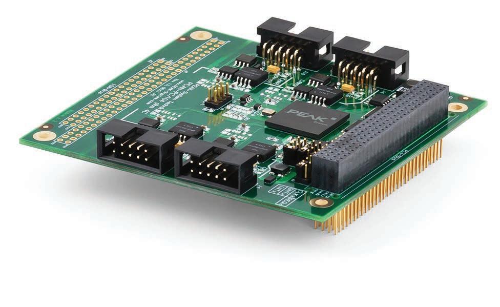
The PCAN-PCI/104-Express card enables the connection of one or two CAN buses to a PCI/104-Express system. Up to four cards can be stacked together. The CAN bus is connected using a 9-pin D-Sub plug on the slot brackets supplied. There is galvanic isolation of up to 500 Volts between the computer and CAN sides.
The package is also supplied with the CAN monitor PCAN-View for Windows and the programming interface PCAN-Basic.
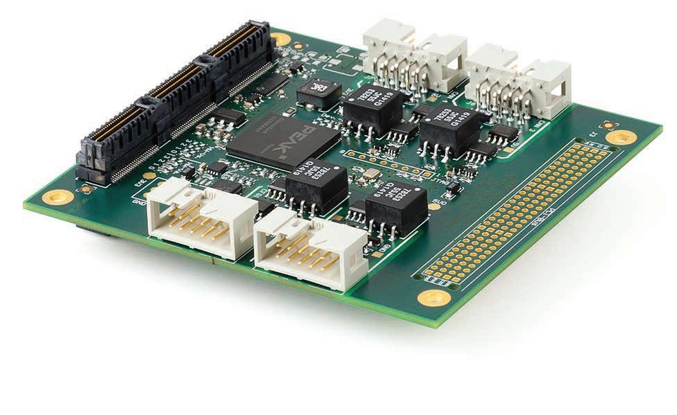
Embedded Computing Design
PCAN-PCI/104-Express Industrial PEAK-System Technik GmbH www.peak-system.com/quick/PC104-4 info@peak-system.com +49 (0) 6151-8173-20 www.linkedin.com/company/peak-system @PEAK_System
Ą PCI/104-Express card, 1 lane (x1) Ą Form factor PC/104 Ą Up to four cards can be used in one system Ą 1 or 2 High-speed CAN channels (ISO 11898-2) Ą Bit rates from 5 kbit/s up to 1 Mbit/s Ą Compliant with CAN specifications 2.0A (11-bit ID) and 2.0B (29-bit ID) Ą Connection to CAN bus through D-Sub slot bracket, 9-pin (in accordance with CiA® 303-1)
Industrial
34 Embedded Computing Design RESOURCE GUIDE | Fall 2022 www.embeddedcomputing.com
PCAN-PCI/104-Express FD
FEATURES:
Ą PCI/104-Express card, 1 lane (x1)
Ą Form factor PC/104
Ą Up to four cards can be used in one system
Ą 1, 2, or 4 High-speed CAN channels (ISO 11898-2)
Ą Complies with CAN specifications 2.0 A/B and FD (ISO and Non-ISO)
Ą CAN FD bit rates for the data field (64 bytes max.) from 20 kbit/s up to 12 Mbit/s
Ą CAN bit rates from 20 kbit/s up to 1 Mbit/s
Ą Connection to CAN bus through D-Sub slot bracket, 9-pin (in accordance with CiA® 303-1)
Ą FPGA implementation of the CAN FD controller
Ą Microchip CAN transceiver MCP2558FD
Ą Galvanic isolation on the CAN connection up to 500 V, separate for each CAN channel
Ą CAN termination and 5-Volt supply to the CAN connection can be activated through a solder jumper
Ą Extended operating temperature range from -40 to 85 °C (-40 to 185 °F)
Ą Optionally available: PCI-104 stack-through connector
PEAK-System Technik GmbH
www.peak-system.com/quick/PC104-5
CAN FD Interface for PCI/104-Express
The PCAN-PCI/104-Express FD allows the connection of PCI/104Express systems to CAN and CAN FD buses. Up to four cards can be stacked together. The CAN bus is connected via 9-pin D-Sub con nectors to the supplied slot brackets. There is a galvanic isolation between the computer and the CAN side up to 500 Volts. The card is available as a single, dual, or four-channel version.
The monitor software PCAN-View and the programming interface PCAN-Basic are included in the scope of supply and support the new standard CAN FD.
info@peak-system.com
www.linkedin.com/company/peak-system
+49 (0) 6151-8173-20
@PEAK_System
Processing:
nanoX-EL, COM Express Mini Size Type 10 Module
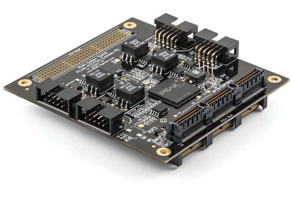
ADLINK nanoX-EL supports 6th generation Intel Atom x6000 processors (Elkhart Lake) combined with Intel UHD graphics at low power envelope and high speed interfaces. nanoX-EL modules support In-Band ECC DDR4 memory up to 16GB, TCC and 2.5GbE with optional TSN and are also available in rugged operating temperature range and low power envelope, making them a perfect match for mission critical fanless edge computing applications that require reliability at all times.
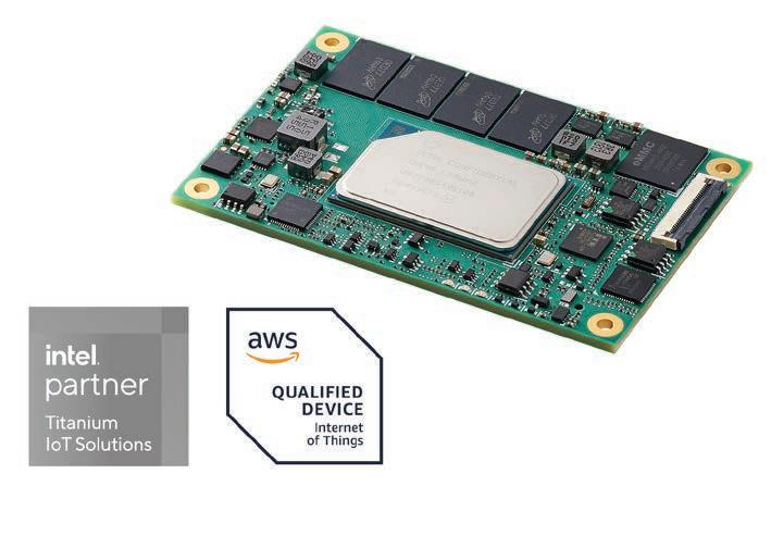
The nanoX-EL is the first COM Express Type 10 Mini Computer-on-Module on the market to support Intel ATOM x6000E series quad core embedded SoC. It is specially designed for industrial embedded applica tions requiring up to 10 years long life, high MTBF and strict revision control. It also provides standard support for up to 16GB LPDDR4, IBECC, TCC and 2.5GbE with optional TSN, ultra-low power and passive cooling, making the ATOM x6000E based module well suited for compact mission critical application in harsh environments.
With integrated UHD graphics, the nanoX-EL supports up to three independent 4K60 displays via DP, HDMI, LVDS or eDP, it is a first for this family of mini sized embedded modules. The nanoX-EL, offers a wide range of high speed interfaces, including one 2.5GbE Ethernet with TSN support, 4x PCIe x1 Gen3 lanes, 2x USB 3.2 10Gbps, 6x USB 2.0. The module can be purchased as COM Express Type 10 Starter Kit Plus devkit that includes everything needed to go live in minutes: nanoX-EL module, miniBASE-10R carrier board, power adapter, debug board and cabling.
FEATURES:
Quad-core Intel Atom® Processor SoC, Burst Frequency up to 3.0GHz
Intel® Gen11 LP GFX for AI inference based on OpenVINO
In-band ECC, up to 16GB LPDDR4 at up to 4267 MT/s
TCC and 2.5GbE with TSN
Real-time I/O via ARM Cortex-M7 processor
USB 3.2 10Gbps
source=ecd&utm_medium=directory&utm_campaign=aati-ecd-elkhart-lake
+1-800-966-5200

Embedded Computing Design
Embedded
x86 ADLINK Technology www.adlinktech.com info@adlinktech.com
www.linkedin.com/company/adlink-technology @ ADLINK_Tech
Ą
Ą
Ą
Ą
Ą
Ą
https://www.adlinktech.com/Products/Computer_on_Modules/COMExpressType10/nanoX-EL?lang=en&utm_
Industrial
www.embeddedcomputing.com Embedded Computing Design RESOURCE GUIDE | Fall 2022 35
IIoT devices run longer on Tadiran batteries.

Remote wireless devices connected to the Industrial Internet of Things (IIoT) run on Tadiran bobbin-type LiSOCl2 batteries.
Our batteries offer a winning combination: a patented hybrid layer capacitor (HLC) that delivers the high pulses required for two-way wireless communications; the widest temperature range of all; and the lowest self-discharge rate (0.7% per year), enabling our cells to last up to 4 times longer than the competition.
Looking to have your remote wireless device complete a 40-year marathon? Then team up with Tadiran batteries that last a lifetime.
* Tadiran LiSOCL2 batteries feature the lowest annual self-discharge rate of any competitive battery, less than 1% per year, enabling these batteries to operate over 40 years depending on device operating usage. However, this is not an expressed or implied warranty, as each application differs in terms of annual energy consumption and/or operating environment.
Tadiran Batteries 2001 Marcus Ave. Suite 125E Lake Success, NY 11042 1-800-537-1368 516-621-4980 www.tadiranbat.com PROVEN 40 YEAR OPERATING LIFE *
ANNUAL SELF-DISCHARGE TADIRAN 0.7% Up to 3% COMPETITORS
