


Future-proof your designs with WINSYSTEMS’ rugged embedded computing solutions designed for highly reliable operation in harsh environments. Our products enable a wide range of applications from EV Charging to factory automation, robotics, industrial IoT, and Edge computing.


US-made COM Express Type 6 Compact and Type 10 Mini Modules and Carrier Boards
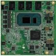
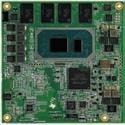
Rugged highly reliable COM modules featuring Intel® Atom® E3900 and 11 Gen CORE™ i3/i5/i7 processors with on-board discrete TPM 2.0 hardware security and industrial temp rating.
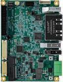
Tiny Pico-ITX SBC: ITX-P-C444
Low power industrial-rated SBC with NXP ® i.MX 8M series processor, on-board discrete TPM 2.0 hardware security, dual Ethernet, industrial connectors and I/O
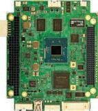
PC/104-Plus SBC: PPM-C407

Low power industrial-rated SBC with Intel® Atom® E3800 series processor, Gigabit Ethernet
EMBEDDED COMPUTING BRAND DIRECTOR Rich Nass rich.nass@opensysmedia.com
SENIOR TECHNOLOGY EDITOR Ken Briodagh ken.briodagh@opensysmedia.com
ASSOCIATE EDITOR Tiera Oliver tiera.oliver@opensysmedia.com
ASSOCIATE EDITOR Taryn Engmark taryn.engmark@opensysmedia.com
PRODUCTION EDITOR Chad Cox chad.cox@opensysmedia.com
TECHNOLOGY EDITOR Curt Schwaderer curt.schwaderer@opensysmedia.com
CREATIVE DIRECTOR Stephanie Sweet stephanie.sweet@opensysmedia.com
WEB DEVELOPER Paul Nelson paul.nelson@opensysmedia.com
EMAIL MARKETING SPECIALIST Drew Kaufman drew.kaufman@opensysmedia.com
WEBCAST MANAGER Marvin Augustyn marvin.augustyn@opensysmedia.com
DIRECTOR OF SALES Tom Varcie tom.varcie@opensysmedia.com (734) 748-9660
DIRECTOR OF SALES ENABLEMENT Barbara Quinlan barbara.quinlan@opensysmedia.com
AND PRODUCT MARKETING (480) 236-8818
DIRECTOR OF MARKETING Eric Henry eric.henry@opensysmedia.com
OPERATIONS & AUDIENCE DEVELOPMENT (541) 760-5361
STRATEGIC ACCOUNT MANAGER Rebecca Barker rebecca.barker@opensysmedia.com (281) 724-8021
STRATEGIC ACCOUNT MANAGER Bill Barron bill.barron@opensysmedia.com (516) 376-9838
STRATEGIC ACCOUNT MANAGER Kathleen Wackowski kathleen.wackowski@opensysmedia.com (978) 888-7367
SOUTHERN CAL REGIONAL SALES MANAGER Len Pettek len.pettek@opensysmedia.com (805) 231-9582
INSIDE SALES Amy Russell amy.russell@opensysmedia.com
STRATEGIC ACCOUNT MANAGER Lesley Harmoning lesley.harmoning@opensysmedia.com
EUROPEAN ACCOUNT MANAGER Jill Thibert jill.thibert@opensysmedia.com
TAIWAN SALES ACCOUNT MANAGER Patty Wu patty.wu@opensysmedia.com
CHINA SALES ACCOUNT MANAGER Judy Wang judywang2000@vip.126.com
PAGE ADVERTISER
21 BlackBerry QNX –Enabling Safety, Security and Reliability in Embedded Software Development
1 Clarinox Technologies –The Simplified Embedded Wireless Ecosystem by Clarinox
1 Digi-Key Corporation –Development Kit Selector
27 Kontron – Speakout: Emerging Trends In the Module Industry
27 Kontron – Speakout: Motherboards that meet your every need: Kontron’s extensive line of high-performance boards
15 NI (National Instruments) –LabVIEW
56 Tadiran – IIoT Devices Run Longer on Tadiran batteries BlackBerry QNX
9 Vector Elect –VME/VXS/cPCI Chassis, Backplanes & Accessories
1 Wind River –
From the leading RTOS provider, new ways to buy
2 WinSystems –Embed Rugged Reliability
Facebook.com/Embedded.Computing.Design
@Embedded_comp
WWW.OPENSYSMEDIA.COM
PRESIDENT Patrick Hopper patrick.hopper@opensysmedia.com
EXECUTIVE VICE PRESIDENT John McHale john.mchale@opensysmedia.com
EXECUTIVE VICE PRESIDENT AND ECD BRAND DIRECTOR Rich Nass rich.nass@opensysmedia.com
VITA EDITORIAL DIRECTOR Jerry Gipper jerry.gipper@opensysmedia.com
MES ASSISTANT MANAGING EDITOR Lisa Daigle lisa.daigle@opensysmedia.com
TECHNOLOGY EDITOR – WASHINGTON BUREAU Dan Taylor dan.taylor@opensysmedia.com
GRAPHIC DESIGNER Kaitlyn Bellerson kaitlyn.bellerson@opensysmedia.com
FINANCIAL ASSISTANT Emily Verhoeks emily.verhoeks@opensysmedia.com
SUBSCRIPTION MANAGER subscriptions@opensysmedia.com CORPORATE
www.linkedin.com/showcase/ embedded-computing-design/
www.youtube.com/c/ EmbeddedComputingDesign
EMBEDDED COMPUTING DESIGN ADVISORY BOARD
Ian Ferguson, Lynx Software Technologies
Jack Ganssle, Ganssle Group
Bill Gatliff, Independent Consultant
Andrew Girson, Barr Group
David Kleidermacher, Google
Jean LaBrosse, Independent Consultant
Scot Morrison, Siemens Digital Industries Software
Rob Oshana, NXP
Kamran Shah, Klick Health
As the automotive industry faces escalating security regulations, there is a corresponding surge in the need for penetration testing, or “pentesting.” Utilizing remote penetration testing and automation tools represents a significant advancement in the realm of automotive security, as it leads to quicker pentest execution and reduced expenses. Read some of the different approaches for advancing the field of automotive penetration testing on page 10.
Executive Vice President How Software Redefines the Value of the Automotive Industry


Tune In: https://embeddedcomputing.com/ application/automotive/how-softwareredefines-the-value-of-the-automotive-industry
Exploited: Netgear Nighthawk RAX30
Read Now: https://embeddedcomputing.com/ technology/security/network-security/ exploited-netgear-nighthawk-rax30

Surviving the Semiconductor Shortage with SoMs

Tune In: https://embeddedcomputing.com/ technology/processing/compute-modules/ surviving-the-semiconductor-shortage-withsoms
Published by:
2023 OpenSystems Media®
© 2023 Embedded Computing Design
All registered brands and trademarks within Embedded Computing Design magazine are the property of their respective owners.
ISSN: Print 1542-6408
Online: 1542-6459

RISC-V is the hot thing in embedded these days, it seems, with news hitting every day. We’ve looked at some of the key tools and players in the RISC-V space, and even seen several major players make moves this week.
One of the bigger announcements in RISC-V news we’ve seen recently came from a recent partnership between some of the biggest automotive chip suppliers. According to this announcement, Infineon, Nordic Semiconductor, NXP Semiconductors, Qualcomm, and Robert Bosch have jointly invested in a new company based in Germany with the goal of advancing global RISC-V adoption.
It seems that the venture will act as an accelerator for the “commercialization of future products based on the open-source RISC-V architecture,” the release stated.
Now, nominally, the group is open to exploring all sorts of industries ripe for RISC-V, but this particular grouping begs the question: Is the automotive industry getting ready to move? Will the automotive OEMs, dare I say, take a ... RISC?
Research group Semico thinks the global automotive market is ready. According to a recent report from the firm, the interest in RISC-V stems partially from the semiconductor supply chain shortages that have been occurring for nearly 5 years now.
“Against this backdrop of architectural and functional exploration are the current supply problems of semiconductors aimed at automotive applications,” said Rich Wawrzyniak, Principal Analyst for SoC and ASIC Research at Semico. “In order to secure a steady supply of the semiconductors needed to produce their vehicles in a timely manner, most, if not all, of the automotive manufacturers have embarked on creating their own internal SoC design groups with the intention of using the silicon foundry network to supply the parts.”
Those internal SoC groups will certainly be looking at RISC-V as an option, and with the new German supergoup of chipmakers in play, that option will look even more viable. Bill Stewart, Vice President of Automotive Americas Marketing at Infineon, is optimistic about the possibilities for RISC-V.
“We see RISC-V as a potential alternative for future CPU core roadmaps. Obviously, we’re making an investment in it, so we see it as viable,” he said. “The automotive OEMs are going to a software-defined vehicle architecture. They’re all investing a lot in software right now.”
As they move into creating their own software and hardware, automotive OEMs are looking for reliable, certifiable standards, and RISC-V is diligently offering one that is paired with being an open architecture – and all the customization and (potential) cost-savings that go along with it.
RISC-V International, the organization driving RISC-V adoption and standardization globally, has been preparing to bring the automotive industry inside. In a blog post from March, it specifically calls out how the technology is suited to carmakers’ needs. “Designers can leverage RISC-V in creating Systems-on-Chips (SoCs) for automotive applications that not only meet performance/ cost/power requirements, but also have a high degree of code portability.”
The post goes on to advocate for RISC-V in safety systems like Advanced Driver-Assistance Systems (ADAS) and autonomous vehicles, in addition to in-vehicle infotainment (IVI) systems that are becoming ever-more sophisticated with advanced displays, connectivity, over-the-air updates, personalized experiences, and even gaming.
It’s not only the chipmakers that are getting in on the action, either. Lars Bergstrom, Director of Engineering at Google, announced in 2022 that Google will support RISC-V in Android ecosystems. And if you look into the existing RISC-V ecosystem, the major players have been building and getting loaded up for quite some time.
As an example, SiFive and IAR have partnered to target automotive with the mating of the SiFive RISC-V Automotive CPU IP and the IAR toolchain, which together offer a set of pre-certified development tools that can ease the rigorous certification process in the automotive sector.
It’s not all settled yet, though. “There’s still a lot to work out and a lot of uncertainty,” Stewart said. The main challenge, as he sees it, will be getting standardization established. “There are a lot of potential applications for RISC-V, and we can’t have RISC-V implementations coming from a bunch of different places. That not standardization.”
The interest and investment are certainly there on the embedded technology side, but the major OEMs have not been as vocal. No major manufacturer has announced a move to RISC-V yet, so we’ll have to wait and see.
Is automotive ready for RISC-V? Hard to say, but it can’t be denied that the RISC-V players are eager to hit the road.
 By Dunstan Power, ByteSnap
The UK has committed to ban the sale of new petrol and diesel cars and vans by 2030 in line with its climate goal of net zero emissions by 2050.
The move to electric vehicles is unfaltering, but what kind of strain to the electrical grid will be created by at least 10 million more EVs in the next decade? Can the grid cope? How can there possibly be any synergy between climate goals and the need to charge millions of new electric vehicles?
These are prudent questions given that in 2022 the Russia-Ukraine conflict quickly resulted in energy supply concerns so severe that three-hour planned power cuts were expected during the winter.
There are currently over 660,000 batteryelectric vehicles (BEVs) in the UK and an additional 445,000 plug-in hybrids (PHEVs). Per LGV and the Energy Savings Trust (EST), it’s estimated there will be between 8 and 11 million electric or hybrid cars on UK roads by 2030. By 2040, this number could reach 25.5 million. This is gargantuan growth but moving to vehicles with net zero emissions is a critical part of the UK’s overall net zero goal. Similar transitions are planned elsewhere around the globe; the U.S. aims for half of all new vehicle sales to be electric by 2030.
Imagine the demand on the grid as 10 million more electric vehicles hit the road. What happens to the power grid if all those vehicles are plugged in to charge at the same time? Overload, right?
If the 32 million cars currently in the UK were electric, the demand for charging them, if they were all plugged in at the same time, would equate to 229GW. The capacity of the National Grid in 2020 was 75.8GW.
In reality, the chances of every EV charging at the same time are extremely slim, though not impossible. Some will be driven, parked, or used once in a while and charged much less often. Others will be charged at work, at the supermarket, or at home overnight. In the near future,
EVs may charge from renewable energy sources, serve as battery stores, and sell their power back to the grid when energy demand peaks.
Experts are not expecting electric vehicle charging to overload the grid and there are number of reasons for this confidence. In August 2022, the National Grid described the issue of the grid not being “able to handle the increase in EVs,” as a myth. The National Grid reiterated earlier commentary that the shift to EVs is gradual, renewable energy sources are being developed, and “we’re constantly evolving the electricity grid.” The issue of developing the grid, nationally and locally, is critical though. Local substations, transformers, and power distribution networks will all require significant updating.
According to the National Grid, electricity demand peaked in the UK at 62GW in 2002 and has fallen by around 16% since, because energy efficiency has improved. It estimates that a complete shift to EVs would only increase demand by around 10%, putting consumption still well below the 2020 peak.
There is another reasonable calculation, as per Forbes. This puts average EV consumption at 3.5 miles per kWh and an average user distance per annum of 7,400 miles, so each car will consume an average of 2,114kWh of energy per year. Multiplied by 32,697,408 vehicles gives total EV consumption of 69TWh. The UK produced 323TWh of power in 2019. EVs won’t draw all the grid’s power, but they may require additional capacity that could come from further energy efficiencies elsewhere or from renewables.
An additional problem for the power grid is that EV chargers are designed to deliver a controlled current to lithium-ion batteries. EV charge current isn’t flexed when demand to the grid is high, EV chargers continue to pull power at the same rate. This contrasts with traditional domestic high-energy appliances like ovens and kettles, which will reduce power draw in times of grid stress.
Balancing Demand to the Grid – Smart Charge Control and Charge Timing
Energy stakeholders are well aware of the theoretical strain on the grid should many EVs be charging concurrently, so regulations are being built in to prevent such a problem.
The UK government has introduced its Electric Vehicle Smart Charge Points Regulations for 2022 and beyond. The regulations cover private EV charge points and smart cables for EV charging, and they ensure EV charge points have smart functionality. This functionality allows for EV charging to happen when there is less demand on the power grid, and for charging to pause when demand is high. The U.S. has its Smart Chargers and Time of Use Rate programs to achieve similar results.
On January 17, 2023, the UK government and Ofgem published the Electric Vehicle Smart Charging Action Plan. The plan’s goal is to make smart charging the “preferred method of long duration charging by 2025.” The plan is supported by further investment of £16 million in funding from the Net Zero Innovation Portfolio (NZIP) for smart charging technologies. Based on the plan’s release:
“The government and Ofgem will seek to remove the barriers that currently prevent the full development of a diverse and competitive smart charging market, while making sure the energy system is ready to respond to the upturn in energy demand that electric vehicles will bring.”
We may be some way from an entirely smart grid scenario where the electricity grid communicates fluently with smart chargers to automatically manage charging times. A scenario where charging switches off when demand is high or supply low, and charging is enabled off-peak or when there is excess energy to the grid, will certainly be the ultimate goal.
Governments and energy stakeholders want to avoid high volumes of EV charging at peak times. In the UK, energy usage peaks between 5pm and 8pm as it gets dark and people return home from work, cook, and finish household tasks or plug in additional devices. Outside of EV regulations, energy companies are already rewarding households that can cut energy use during peak times.
UK electricity tariffs are cheaper at night, which will encourage off-peak charging and there are likely to be further incentives for off-peak charging as EV numbers grow. Peak charging could also be discouraged by the implementation of higher electricity tariffs during this time.
Overcoming EV charging problems, developing EV charging infrastructure, improving grid efficiency and local power infrastructure, and balancing charging demand to power grids are all important components to EV adoption and development. The UK has committed £1.3 billion to developing public and private charge points and has pegged up to £1 billion for the development and production of EV batteries. Ofgem plans to reinforce the UK power distribution network.
The proportion of energy generated by renewable sources is growing quickly. Some of these sources can generate additional grid capacity at certain points in time. Solar energy can pick up some slack from daytime demand. Windy periods, or windy nights, may be able to meet additional demand, or night-time demand from EV charging.
Effectively coordinating peaks in both energy supply and demand could be key to meeting EV charging requirements whilst balancing climate goals – without overloading the grid.
The Potential of V2H and V2G
Vehicle-to-Home (V2H)
Battery capacity must be substantial for EVs to “go the distance,” with petrol and diesel vehicles, and innovation in battery technology is pushing this capacity upwards.
This capacity means an EV battery has the potential to be used as a flexible energy storage device or home battery system that can help offset power supply and demand fluctuations. When there is excess or cheap power, EVs can be charged. When power demand is high, or expensive, EV batteries can give power back to homes and even back to the grid.
In a V2H scenario, an EV can be charged with excess solar power generated by the home. When it’s dark, or cloudy, the EV can give the stored power back, saving the household from purchasing electricity.
In 2018, OVO Energy and Imperial College London declared V2G could have the potential to save the UK energy network £3.5 billion per year. OVO Energy and Nissan conducted a three-year trial after installing 330 bidirectional chargers in UK homes. They concluded the homes could save up to £725 annually on their electricity bills if they gave (or sold) stored power from their EVs back to the grid during peak hours.
There are several barriers to V2H and V2G. Bidirectional chargers are large, unsightly, and costly. The number of homes generating their own power is still relatively few, and
few current EV models support bidirectional charging technology. Plus, given the complexity of power networks and the number of EV makers, the diversity of EV charging, and the number of electricity companies involved, coordinating energy price and exchange is an incredibly complicated operation.
Virtual power plants are pitched as a solution to managing grid pressure and would form part of a smart distribution network. The Power Potential R&D, a project run by UK Power Networks and National Grid ESO, plans for renewable power operators within a region to be able to produce energy but also to contribute to correcting problems with supply or voltage that occur within a network.
Virtual power plants can also consist of groups of EV chargers and enable V2G. EV energy is trialing such systems that shift loads away from evening peaks, or that prioritize charging when renewables are creating a surplus.
Our net-zero emissions future and shift to EVs may rely predominantly on the strength of the technology supporting this societal change. Energy distribution networks and entire power grids must become fully smart.
Eliminating energy waste, channeling surplus energy, and adjusting supply when demand is high can all be controlled automatically by integrated smart technologies.
This smart future is immediately possible. Bringing it to fruition, however, will rely on all stakeholders developing and implementing technologies that share the same design principles. Technologies must be able to easily communicate and work with one another, right from power plants down to EVs, chargers, and other devices at home.
Dunstan Power, Director at ByteSnap Design, is an experienced leader of electronic product design teams. His specialties include project and team management, architecting electronic systems, business development, digital hardware and FPGA design, Product design, and more.

 By Roman Lysecky, BG Networks
As security requirements and legislation for auto manufacturers continue to increase, so does the demand for penetration testing, or “pentesting.” Pentesting is becoming a requirement for all new Electronic Control Units (ECUs) that need to be cyber-secure, but the rising cost of pentesting is a major concern. This is due to the growing number of devices that must be tested, the limited number of available penetration testers with the appropriate skills, and the lack of automated tools.
Remote pentesting and automation tools are a game-changer for automotive security because it results in shorter times to complete pentests and lower costs.
The traditional approach requires pentesters to have physical access to the ECUs being tested. This can be timeconsuming and expensive. Remote pentesting eliminates these challenges by allowing pentesters to test ECUs from anywhere in the world and, when combined with automation, provides several other advantages. These benefits include:
› Eliminating the need to ship ECUs or for pentesters to travel.
› Sharing a single ECU between multiple pentesters.
› Around the clock testing with pentesters in different time zones.
› Fewer ECUs needed for testing.
› Automation of repeatable tests (e.g., fuzzing, scanning).
› Shift left. Run tests earlier in the development cycle including CI/CD regression testing.
› Validation and verification of security features.
› Real-time reporting of results.
› New automated ways of reporting vulnerabilities to management systems.
› Aligns with ISO SAE 21434 specified testing requirements.
› Integration of pentesting with incident response for vulnerability validation.
Remote pentesting allows skilled researchers to contribute from anywhere in the world, without being limited by time zones or distance. This helps to bridge the cybersecurity skills gap caused by a limited number of pentesters in a particular area.
Innovative solutions, such as BG Networks’ collaborative and remote pentesting platform, offer a new approach to address the challenges of automotive pentesting. This platform combines a software-managed remote bench with a collaborative testing framework, automation to re-run tests, and logging of results.
By using a remote bench, pentesters can collaboratively test multiple ECUs simultaneously, without the need for physical access. The flexibility of remote access means that testing can take place at any time of the day, providing maximum convenience for both testers and developers. Live reporting of testing results allows engineers to quickly reproduce any findings and address them more quickly.
The automotive industry has increasingly focused on cybersecurity in recent years. This focus has led to the staffing of expert product security teams and

the development of significant cybersecurity capabilities. Regulation has been a driver behind this development. When it comes to critical infrastructure, regulation is needed to ensure that the right level of cybersecurity is included to provide resilience against Advanced Persistent Threat (APT) groups and adversarial nation states.
The key regulations and security standards that have been the driver for cybersecurity in automotive systems are:
› UNECE Regulations UN R155 & UN R156 for Vehicle Cybersecurity
› ISO/SAE 21434 Road Vehicle Cybersecurity Standard, which is the reference implementation for R155 compliance
These regulations require companies to implement a full Cybersecurity Management System (CSMS). This includes development of security from initial stages of design, implementation of cybersecurity features to protect devices from cyberattacks, testing to validate and verify security has been implemented correctly, monitoring for newly exposed vulnerabilities, and an incident response team to quickly remediate any attacks that are detected.
At a high level, a secure development process requires the following steps:
› Performing security threat assessment/risk analysis (TARA) to identify potential vulnerabilities and to guide the implementation of security features. A TARA identifies the right amount of security for the given system considering potential threats and risks including financial, data, operational, and safety impacts.
› Implementing cybersecurity features such as secure boot, authenticated communication, secure key storage, secure software update mechanisms, and device security monitoring.
› Managing supply chain security to ensure vulnerabilities are not introduced when open-source software or commercial third-party solutions are utilized in developing a product.
› Penetration testing to uncover security vulnerabilities.
Without penetration testing, it is impossible to know if a device is truly secure. No one would consider releasing an automotive ECU without extensive testing of core features for functionality and safety. Penetration testing provides analogous testing for security features of an ECU.
Furthermore, ISO/SAE 21434 specifies testing for “unidentified weaknesses,” and cites penetration testing as a method for doing this. Given that all new vehicles in the EU need to be R155 certified by July 2024, there is an increasing need for pentesting.
Penetration testing is performed by personnel who have not been involved in the design of the product and that have a unique skill set. Pentesters essentially act as hackers and use the same techniques to identify cybersecurity vulnerabilities and potential attacks. This is a critical step in ensuring that security has been implemented correctly and there are no open security gaps. It is very easy to make a mistake that leads to a significant vulnerability such as:
› Not setting the secure boot mode bit in an embedded processor
› Forgetting to remove engineering test code from the production code release
› Using keys that were meant to be temporary and are not secure
› Forgetting to close all unused network ports
› Using default or easy to guess passwords
› Allowing root privilege in a shell
› Not locking JTAG
› Software buffer overflows
These are all common security mistakes that pentesting can uncover. A simple security mistake, such as these, can turn into a serious safety and operational problem.
Pentesters simulate real-world attacks and attempt to exploit vulnerabilities in the device’s firmware, software, and hardware. The goal is to identify weaknesses that could be exploited by hackers to gain unauthorized access to the ECU or its data, use it as a pivot point to attack other ECUs in the vehicle, or most seriously, compromise the integrity of an ECU that controls a physical actuator (steering, breaking, acceleration, ADAS, etc.).
Pentesting for automotive ECUs typically involves the following steps:
1. Reconnaissance: Gathering information about the device, such as its firmware version, supported interfaces, and software configuration.
2. Identification of vulnerabilities: using hacking tools and clever tricks of the trade to identify vulnerabilities and weaknesses. This can take many forms:
a. Privilege escalation: Attempting to gain administrative access to the device or its data.
b. Running tests/attacks against known protocols and interfaces using hacking tools.
c. Scanning vulnerability databases for known vulnerabilities in the software components running on the ECU.
d Reverse engineering the code running on the ECU to search for weaknesses and vulnerabilities.
3. Exploitation: Attempting to exploit vulnerabilities found during the identification phase. This includes chaining vulnerabilities that could lead to very significant exploits.
4. Post-exploitation persistence: Attempting to maintain access to the device, exfiltrate data from the device, or use it as a pivot point to attack other ECUs in the vehicle.
5. Reporting: Documenting the vulnerabilities found and providing recommendations for remediation.
Once vulnerabilities have been identified, these weaknesses can be remediated to eliminate the potential for adversarial exploitation to occur in the wild.
Pentesting for ECUs requires specialized knowledge and skills, including knowledge of ECU device architecture, firmware analysis, reverse engineering, software development, hardware, network, and automotive protocols. It is typically performed by experienced security professionals with specialized training in software, IoT, embedded systems, and automotive security.
Pentesting for ECUs presents several unique challenges, which can lead to high costs and long schedules, including:
1. Heterogeneity of ECU architectures: ECUs are built on a wide range of hardware and software platforms/operating systems, and utilize a variety of communication protocols and buses, some of which are unique to automotive ECUs. This makes it challenging to develop standardized testing methodologies that can be applied across all devices.
2. A large attack surface with many types of interfaces: Knowledge of a wide array of interfaces and associated software stacks is needed to test
for weaknesses. Interfaces include Ethernet, CAN, USB, JTAG, LIN, cellular, Wi-Fi, Bluetooth, SD Card, V2X, and EV charging interfaces.
3. Heterogeneity of ECU suppliers: Every vehicle has many ECUs, and ECUs within a given vehicle are often developed by numerous tier 1 suppliers. As a result, multiple software stacks for the same interface are often independently developed. Each implementation needs to be tested as it may have unique security vulnerabilities.
4. Limited processing power and memory: Many ECUs have limited processing power and memory, which can make it challenging to run vulnerability scanning tools or require more time to craft tests.
5. Components of a larger system: Automotive ECUs are designed to work as components of the overall vehicle. It is necessary to test these ECUs in isolation, but that is not sufficient. Penetration testing must also consider how these devices will be used in the vehicle and what attacks are possible at a system level. For example, what attacks are possible against ECUs connected to a common CAN bus if the infotainment ECU is hacked? This requires additional knowledge of how the overall system operates and what the most significant cyber-risks are at the vehicle level. Challenges are also presented in setting up and running a single ECU that is designed to operate in a large system (e.g., creating needed cable harnesses, providing power, providing the correct message sequences to have the ECU respond, etc.).
Overcoming these challenges requires specialized skills and expertise in automotive ECU security testing, as well as a thorough understanding of the unique characteristics of automotive systems. Pentesters must be able to work with a wide range of tools and techniques to
identify vulnerabilities and provide recommendations for remediation.
Automotive ECUs are subject to a variety of attack types (Figure 1). Attacks may originate on remote networks over a cellular interface. They may also originate from local networks, such as an automotive dealers’ network that is used to update and diagnose vehicles in an auto-shop. Other attacks require a local presence, such as attacks over a Bluetooth interface or physically gaining access to a CAN bus (e.g., removal of a headlight) to steal a vehicle.

Hackers can also compromise a local host, such as an infotainment or telematics ECU and then pivot and use the compromised ECU to find weakness in other ECUs or the automotive OEM’s cloud system. For example, certificates that allow cloud access to millions of vehicles have been found, without adequate cyber-security, in telematics units. Older remote keyless entry protocols have been shown to be insecure against man in the middle attacks. Finally, hackers can perform physical attacks by connecting directly to an ECU bus or memory and performing fault injection attacks or reading data directly from the device.
Pentesters must consider each attack type when assessing the security of automotive ECUs.
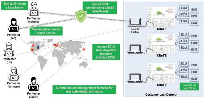
To enable pentesting at scale, better tools are required (Figure 2). BG Networks’ remote pentesting platform is designed to address these challenges. This platform
includes a remote workbench, supporting remote desktop access via VPN enabling pentesters to access an ECU as if it were in their local lab. The solution supports:
› Access to ECUs by local and remote pentesters.
› Automation of scanning and fuzzing tests.
› Remote access to debugger interfaces & buses (LIN, CAN, and Ethernet) on the ECU.
› Remote control of power to the ECU.
› Spectator mode for training and demonstration of discovered vulnerabilities.
› Logging of all activity during testing.
The solution also provides a testing framework that enables collaboration among pentesters, security engineers, and ECU hardware & firmware engineers.
The workbench is designed specifically for ECU pentesting and provides multiple automotive interfaces that can be utilized by pentesters. These include LIN, CAN, and Ethernet. It also supports standard debug interfaces, such as JTAG. This allows pentesters to execute tests and monitor interfaces, just as they would if they had physical access to the ECU.
The platform also allows tests to be scripted for repeatability. Once a test is developed, it can be added to a set of regression tests that are run each time a new version of the ECU hardware, firmware, or software is released. As more tests are developed, testing moves from custom testing of the new capabilities to an automated process in which known tests are automatically run.
Summary
The automotive industry is adapting to new legislation and industry standards requiring manufacturers to be proactive in adding security to their devices. Penetration testing is now a must-have for automotive ECUs, but current pentesting processes don’t scale to meet the growing needs of the industry.
Automated tools for pentesting are needed. Of particular importance are tools to allow remote penetration testing, and to automate execution of existing tests. A remote workbench to allow testing without physical access to an ECU combined with automation tools will dramatically increase productivity and collaboration, and enable repeatable testing.
Dr. Roman Lysecky is Co-founder and CTO of BG Networks and Professor Emeritus of Electrical and Computer Engineering at the University of Arizona. He is an expert on embedded systems, IoT security, medical device security, automated threat detection and mitigation, performance and energy optimization, and non-intrusive observation methods.
The BG Networks workbench enables pentesting of ECUs by local and remote teams. FIGURE 2 Multiple attack types must be considered when pentesting automotive ECUsThere is a seemingly endless number of RTOSes used with embedded MCUs, most of which have their own proprietary functionality as well as a unique API. Some of the APIs are good, and some not quite as good. In reality, the delta between a good and less-good RTOS API is quite small – most RTOS APIs will do the trick. As I look back on my last 30+ years, I’ve come to realize propriety RTOS APIs have had and continue to have a profound negative impact on embedded development and on our industry as a whole.
First and foremost, the proprietary RTOS API represents a lock-in for the application firmware. Code written using a proprietary RTOS API must be changed in order to move to a different RTOS. Worse, the changes required to move to another RTOS can be daunting. Some RTOS vendors have added an adaptation layer in an attempt to support other APIs. However, this solution is less than ideal as it often tries to fit a square peg in a round hole. Not to mention additional layers greatly increase overhead as well as complexity of the RTOS, which in turn can result in errors.
In any case, not being able to easily migrate application code can severely limit the evolution of a product. For example, if an application is dependent on RTOS XYZ and it doesn’t support the latest and greatest processor, the application either needs to modify their code base to move to another RTOS, wait until RTOS XYX adds support, or just give up. Similarly, migrating a RTOS XYZ-based application to embedded Linux (another very common situation), is difficult because multithreading in embedded Linux is based on the POSIX pthreads API. A standard RTOS API would help eliminate lock-in, thereby making embedded applications more portable and enhancing their future evolution.
Proprietary RTOS APIs also require extensive training. Most developers using an RTOS for the first time have to spend significant cycles learning the proprietary
RTOS API. Even embedded developers using FreeRTOS or Microsoft’s Azure RTOS ThreadX – both popular embedded RTOSes, each having their own proprietary API – represent a fairly small percentage of the total number of developers. The point here is that proprietary RTOS APIs necessitate learning, which costs companies time and money. An industry standard RTOS API would reduce training and, as a result, save money and improve device maker’s time-to-market.
Another issue is that some device makers have product families that span both MCU and MPU processors, typically with different functionality and price points. Their MPU-based products frequently use some flavor of embedded Linux. For these companies, having to maintain separate development teams (and code bases) because of a proprietary RTOS API is both difficult and costly. With a standard RTOS API, application code could be instantly shared between MPUand MCU-based projects, improving the entire development process, from coding and testing to product release.
What Should the Standard RTOS API Be?
Before we go further, credit should be given to Arm, since they identified this problem in the embedded industry many years ago and even tried to address it with the CMSIS-RTOS API. Unfortunately, the CMSIS-RTOS API is ultimately yet another proprietary RTOS API.
Back to what the standard RTOS API should be. Amusingly, the answer has been right in front of us for many years: The standard RTOS API should be the same industry standard POSIX pthread API, which is already part of every embedded Linux distribution, as well as every university computer science curriculum. Since embedded Linux represents 70% of the embedded designs, it’s easy to argue that the POSIX pthread API is already the RTOS API standard in the embedded space and what most developers are already familiar with.
Furthermore, the POSIX pthread APIs have been tested on UNIX/Linux systems for over 30 years. Coupling hard real-time capabilities with this industrial standard API promises embedded developers the best of both worlds. Our industry just needs the various RTOS providers to natively adopt it. Uniting the embedded industry on the POSIX pthread API standard would eliminate lock-in, accelerate embedded product evolution, reduce training, and instantly enable code sharing and migration between MCU- and MPU-class devices – all of which represents a significant step forward for the embedded industry.
Bill Lamie, President and CEO of PX5 RTOS, has been in the commercial RTOS space for over 30 years – first with Accelerated Technology (acquired by Siemens) and then with Express Logic (acquired by Microsoft). Bill was the sole author of Nucleus and ThreadX.
Accelerating
For over 35 years, engineers have turned to LabVIEW as their tool of choice for developing automated test systems.
Download today at ni.com/labview
Pytest is a command-line tool that finds, runs, and reports the results of tests you’ve written. It is suitable for all levels and types of the testing process. Pytest can be used by developers and designers, quality assurance teams, independent testing groups, and open-source projects.
Today’s modern businesses require faster software feature releases to produce high-quality products and to get to market quickly without sacrificing software quality. To ensure successful deployments, the accelerated release of new features or bug fixes in existing features requires rigorous end-to-end software testing.
While manual testing can be used for small applications or software, large and complex applications require dedicated resources and technologies like python testing frameworks, automation testing tools, and so on to ensure optimal test coverage in less time and faster quality releases.
Pytest is a testing framework that allows individuals to write test code in Python, enabling you to create simple and scalable test cases for databases, APIs, and user interfaces. Pytest is primarily used for writing API tests. It aids in the development of tests ranging from simple
unit tests to complex functional tests. According to a report published by Future Market Insights, the global automation testing market is expected to grow at a CAGR of 14.3% registering a market value of US$ 93.6 billion by the end of 2032.

Selection of the right testing framework can be difficult and relies on parameters like feasibility, complexity, scalability, and features provided by a framework. Pytest is the go-to test framework for a test automation engineer with a good understanding of Python fundamentals. With the Pytest framework, you can create high-coverage unit tests, complex functional tests, and acceptance tests (Figure 1). Apart from being an extremely versatile framework for test automation, Pytest also has a plethora of test execution features such as parameterizing, markers, tags, parallel execution, and dependency.
› There is no boilerplate while using Pytest as a test framework.
› Pytest can run tests written in unittest, doctest, and nose.
› Pytest supports plugins for behavior driven testing.
› There are more than 150 plugins available to support different types of test automation.
The diagram below shows a typical structure of a Pytest framework.
As shown in the Figure 1 structure, the business logic of the framework core components is completely independent of Pytest components. Pytest makes use of the core framework just like instantiating the objects and calling its functions in the test script. Test script file name should either start with `test_` or end with `_test`. The test function name should also be in the same format. Reporting in Pytest can be taken care of by Pytest-html reporting.
1. Pytest fixtures
The most prominently used feature of Pytest is Fixtures. Fixtures, as the name suggests, are decorator functions that are used in Pytest to generate a specific condition that needs to be arranged for the test to run successfully.
The condition can be any precondition like creating objects of the classes required, bringing an application to a specific state, bringing up the mockers in case of unit tests, initializing the dependencies, etc. Fixtures also take care of the teardown or reverting of the conditions that were generated after the test execution is completed. In general, fixtures take care of the setup and teardown conditions for a test.
Fixture scope
The setup and teardown do not have to be just for the test function. Scope of the setup may differ from a test function to as large as the whole test session. This means the setup-teardown is executed only once per defined scope. To achieve the same, we can define the scope along with the fixture decorator i.e., session, module, class, function.
Fixture usage
Pytest provides the flexibility to use a fixture implicitly or call it explicitly, with the autouse parameter. To call the fixture function by default, the autouse parameter value needs to be set to True, else to False.
2. Conftest.py
All the fixtures that are used in the test framework are usually defined in conftest.py. It is the entry point for any Pytest execution. Fixtures need not be autouse=True. All defined fixtures can be accessed by all the test files. conftest.py needs to be placed in the root directory of the Pytest framework.

3. Pytest hooks
Pytest provides numerous hooks that will be called in to perform a specific setup. Hooks are generator functions that yield exactly once. Users can also write wrappers in conftest for the Pytest hooks.
4. Markers
Pytest provides markers to group a set of tests based on feature, scope, test category, etc. The test execution can be auto-filtered based on the markers. i.e., acceptance, regression suit, login tests, etc.
Markers also act as an enabler for parameterizing a test. The test will be executed for all the parameters that are passed as the argument. Note, Pytest considers a test for one parameter as a completely independent test. Many things can be achieved with markers like marking a test to skip, skipping on certain conditions, depending on a specific test, etc.
5. Assertion
Pytest does not require the test scripts to have their assertions. It works flawlessly with Python inbuilt assertions.
6. Pytest.ini
All default configuration data can be put in pytest.ini and the same can be read by the conftest without any specific implementation.
Pytest supports a huge number of plugins with which almost any level of a complex system can be automated. A major benefit of Pytest is that any kind of implementation of the structure is done using raw Python code without any boilerplate code. It means implementing anything in Pytest is as flexible and clean as implementing anything in Python itself.
Amidst shorter development cycles, test automation provides several benefits that are critical for producing high-quality applications. It reduces the possibility of unavoidable human errors taking place during manual testing methods. Automated testing improves software quality and reduces the likelihood of defects jeopardizing delivery timelines.
Rahul Vala, Principal Engineer at Softnautics, is a solution-focused test automation engineer with 7+ years of experience in systems testing of different types. He possesses high level proficiency in end-to-end systems test automation and framework development of complete IoT ecosystem (web, mobile, end device, cloud) using different types of frameworks with Python.
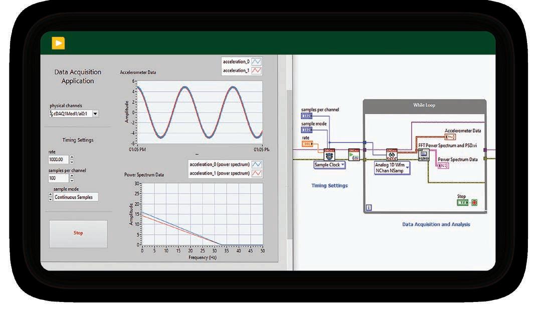
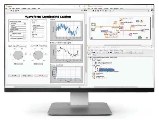
LabVIEW, the graphical programming environment used globally by systems and test engineers (Figure 1), automates and simplifies what would otherwise be a tedious manual process. Developed and maintained by NI, LabVIEW is used to create applications that interact with real-world data or signals, such as measurement or control systems.
When using LabVIEW, users create programs by dragging and dropping different graphical elements onto a block diagram. This would otherwise be achieved by writing lines of code in textbased languages. These graphical elements are wired together to do things like acquire and analyze data and control instruments and processes.
A key benefit of LabVIEW is that it can reduce development time, partly due to its array of pre-built functions. In addition, a lot of the time savings comes from LabVIEW’s user interface and visualization capabilities. If you’re looking to monitor or interact with your test system in any way, LabVIEW has lots of functions for that. If you want to create charts, graphs, lights, or buttons, for example, that’s all readily available so the build is simple. You just drag, drop, move around, and resize as needed.
Candidates for LabVIEW include pretty much anyone doing test or measurement, or looking to connect to an instrument and acquire data. The beauty of LabVIEW is that it can scale from the smallest applications, even a one-time measurement, to a fully automated system with multiple devices.

This is where the tool really shines – when you’re connected to hardware and trying to measure and analyze at the same time, and when you are trying to connect multiple instruments at once. This eliminates the disconnect of going back and forth between tools, say a measurement program and then something else to handle the analysis. And that analysis occurs on the fly in LabVIEW, as the measurements are coming in. From that point, you create a report and automate it.
The “entry point” for LabVIEW occurs the second you need to take a measurement that’s beyond a basic temperature probe, essentially a measurement that needs to be logged at some point to validate and/or verify parts of your design.
While the learning curve for LabVIEW is quite short, unfamiliar or inexperienced developers should expect to take a brief training course, similar to starting any new language. But because the tool is graphical in nature, the training occurs very quickly. The real prerequisite is to understand algorithms and the test systems that are under development. Note that NI has lots of existing content that provide a jump start to just about any design. There’s also a trial version of LabVIEW that users might want
to test drive. And for those that may need a little extra or really want to get into the inner workings of LabVIEW, paid courses are available. It’s quite similar to getting started with a language like Python, to understand simple programming and how to formulate algorithms.
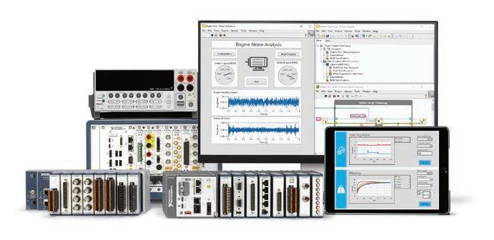
That’s not to say that having some basic programming knowledge wouldn’t come in handy. Keep in mind that graphical programming is somewhat different – easier, but different. It’s a little more intuitive, where you are dragging and dropping functions rather than writing your application line by line and needing to follow a very specific format and syntax (Figure 2).
The learning curve for a seasoned engineer should be a short one. In practice, every function has a help detail to walk you through specifically what that function is and how it should operate. And lots of detailed examples ensure that you’re usually not starting from point 0. While there may not be the exact example you’re looking for available, you can usually get pretty close, where it’s more about tweaking code than writing from scratch.
There is also a loyal community of LabVIEW users that scale across different industries, geographies, and languages that are quite passionate about the tool and typically lend a hand when asked. Note that this is external to NI, but extremely valuable, nonetheless.
The openness of LabVIEW allows it to keep pace with the latest and greatest technologies. Take AI, for example. If your code is already written in another language such as Python, it can be integrated into your existing LabVIEW application.
If you’re focused on one specific measurement using one device, then you may not realize the advantages of LabVIEW. But if you need to build upon that measurement, like connect to other devices, do analysis, or create reports, you can probably do it faster in LabVIEW. And LabVIEW works well if you’re operating with a team of multiple people, locally or in other parts of the world. You can track changes when modifying applications and compare results.
The bottom line is that, if you want to take measurements, analyze data, share results with your team and spend less time developing, LabVIEW is likely your best option.
“THE BEAUTY OF LABVIEW IS THAT IT CAN SCALE FROM THE SMALLEST APPLICATIONS, EVEN A ONE-TIME MEASUREMENT, TO A FULLY AUTOMATED SYSTEM WITH MULTIPLE DEVICES.”
 By Michael De Nil, Morse Micro
The Wi-Fi blackspot problem inside the home has been largely solved by Wi-Fi 6 mesh access points that allocate some of their wireless bandwidth to establish connectivity between mesh network nodes, thus extending the reach of the wireless local area network (WLAN). While this works well in many domestic situations, and for some small offices, it’s not nearly a perfect solution.
On larger properties, Wi-Fi 6 mesh access points still struggle to reliably reach some garages, secondary dwellings, and outdoor locations. This limits reliable connectivity to new Internet of Things (IoT) devices such as remote locking systems and security cameras.
Overcoming the range limitations of current Wi-Fi standards is a major challenge for enabling the IoT applications of the future. The limitations in range come down to simple physics. Wi-Fi 4, 5, and 6 operate in the 2.4 GHz and 5 GHz frequency bands with the more recent Wi-Fi 6E adding the 6 GHz band to the mix. While these higher frequency bands allow wider channels with faster performance, lower frequencies offer better range and penetration. So, today’s Wi-Fi networks, including Wi-Fi mesh systems, are subject to the range limitations of the higher frequency bands.
Wi-Fi HaLow is the latest wireless protocol, certified by the Wi-Fi Alliance and based on the IEEE 802.11ah standard. Wi-Fi HaLow uses lower frequencies and narrower bandwidths, which enable ten times longer reach than conventional Wi-Fi networks that operate at
higher frequencies. While Wi-Fi HaLow removes the need for Wi-Fi meshing for new IoT deployments, especially in nondomestic environments, it also adds key benefits when combined with Wi-Fi 6, or soon Wi-Fi 7 mesh technology.
Operating at sub-GHz frequencies, Wi-Fi HaLow can transmit data over much greater distances and penetrate materials better than other Wi-Fi standards, such as Wi-Fi 4, 5, and 6.
While 5 GHz and 6 GHz Wi-Fi technology can provide multi-Gbps backhaul links between mesh nodes at short distance, the quality of the link quickly deteriorates as Wi-Fi mesh nodes are spaced further apart. In fact, most Wi-Fi mesh access point vendors recommend spacing units not further apart than 10 meters and they do not allow users to set up mesh nodes that are farther apart in order to guarantee reliable connectivity.
Wi-Fi HaLow enables mesh access points to reach farther, creating more robust and reliable infrastructure, even if mesh nodes are spaced further apart. The
sub-GHz link can be used as a secondary backhaul to enable Wi-Fi connectivity in places that are out of reach today.
And while the narrower channels do mean throughput is lower than Wi-Fi 5 and 6, Wi-Fi HaLow devices can still deliver throughputs in excess of 30 Mbps, which is fast enough for bandwidthhungry applications such as audio streaming, video conferencing, or even watching Netflix in HD.
Wireless mesh networking is inherently difficult because it involves the coordination of various nodes to create a reliable and robust network; each needing to adapt to the dynamic nature of wireless networking. Wi-Fi mesh networks are susceptible to interference from other neighboring Wi-Fi devices as well as various other wireless devices in the home, including Bluetooth headsets, Zigbee lightbulbs, or Z-Wave security sensors.
While Wi-Fi mesh access point vendors have helped mask these complexities for the end user, they still struggle when connectivity is lost or is intermittent
between nodes. For example, range issues, traffic volume, or interference can make diagnosing problems difficult or impossible.
Configuring and maintaining wireless mesh networks can be significantly simplified by splitting the high-speed data plane, which inherently relies on a functional mesh, from the control plane, which requires a reliable and robust link between nodes. Wi-Fi HaLow can provide an independent out-of-band radio in each mesh node, enabling direct communication between the master and any of the end nodes. This enables reliable network configuration, problem diagnosis, and recovery, thus enhancing ease of use and optimizing overall Wi-Fi management and performance.
Prepare for the Future of Mesh Networks
International Data Corporation (IDC) forecasts a massive growth in the number of IoT devices that will be connected to networks. It estimates that there will be in excess of 40 billion IoT devices by 2025, potentially generating up to 80 zettabytes of data. Connecting those devices to networks will become a major challenge in the coming years.
Wi-Fi HaLow can free up bandwidth in the higher frequency bands by moving IoT to the sub-1 GHz band and is starting to make its way into many IoT devices because of its advantages in power consumption and range. Therefore, adding Wi-Fi HaLow to mesh access points now will enable those devices to connect without the need for additional network equipment in the future. A mesh node equipped with both Wi-Fi 6
and Wi-Fi HaLow will enable enhanced connectivity for IoT devices while supporting traditional Wi-Fi applications.
The development of mesh networks and the continued evolution of Wi-Fi have been a boon for consumers. Whether people are working from home, enabling smart home devices, boosting coverage in offices, or starting to leverage IoT, extending networks using a standardsbased approach that avoids the costs of cabling and additional switches delivers significant benefits.
Michael De Nil is the CEO, co-founder, and a board member of Morse Micro. He played a key role in the digital chip development of the 802.11 Wi-Fi chips found in most modern smart phones and had 10 years of experience in low-power digital IC design at Imec and Broadcom before founding Morse Micro.
BlackBerry® QNX® is the embedded OS of choice for factory automation systems, medical robots, vehicles, ventilators, train controls, and more. Launch your critical embedded systems faster with our commercial real-time operating system (RTOS), hypervisor, development tools and professional services. Our hypervisor and middleware deliver performance and security and streamline safety certifications.
Embedded systems are more software-driven and complex than ever. BlackBerry® QNX® provides the software foundation and building blocks to help you focus on delivering value-added features and software.

If you’re looking to increase security or safety, or you want to streamline your cross-platform development process, we can help. We provide support for every stage of the product lifecycle and offer professional services and training to give you the additional expertise you need, when you need it.
• Foundation products include the QNX® Neutrino® RTOS, the QNX® Software Development Platform (SDP) with a POSIX-compliant development environment, and the QNX® Hypervisor.
• Safety-certified variants of our products accelerate your certification efforts. Accelerate time to market with software pre-certified to IEC 61508, ISO 26262 and IEC 62304, QNX® functional safety training, and safety services.
• Security – With a microkernel architecture, our RTOS and hypervisor are secure by design. Rely on our fieldproven cybersecurity experts to help protect your systems, including secure over-the-air updates.
• Reliability – The QNX microkernel architecture protects the OS and system from component failure and delivers exceptional performance.
• Scalability – Our fully-managed microkernel RTOS can be duplicated and used across all product lines, so your developers can focus on value-added features, not OS maintenance.
BlackBerry QNX offers customized professional services to bring safe, secure and reliable products to market on time, on budget and with excellent quality. We have decades of experience successfully delivering embedded systems for organizations in multiple industries.
 By Sri Peruvemba, Marketer International
I know 3D display technology has had its skeptics through the decades, and many in the industry have failed in this arena, but I believe 3D display technologies will touch just about every industry, further pushing the boundaries on the human digital experience – from entertainment to medical, military applications, engineering, graphic design, architecture, and more. Like rotary phones, we will forget that we had 2D displays.
However, I admit we are not quite there yet. While there has been significant progress in the display itself, we are not where we need to be to create a massive shift from 2D to 3D. For one thing, both the hardware and the
software need to be dramatically improved (think energy consumption, massive computing needs, for example). The entire industry needs to adopt this transition – from hardware to software to chip makers, and everything in between.
We also need higher resolution displays: 300 ppi to 500 ppi displays, from small to large sizes, to get the best results. Today, we have high resolution displays, but they
tend to be for phones with a notch for the camera or they have to be specially made, which renders them unsuitable for the mass market.
To make really good 3D light field displays, for example, you need large format displays with high resolution, which aren’t easy to come by. Even today, it’s hard to get any better than 8K, which is fine for smaller displays; but for an 85” display, even higher resolution is preferred. To clarify, 8K is plenty of resolution for 2D displays, but barely makes it for 3D.
In a future 3D digital world, our TVs will resemble the theater; the basketball game on TV will resemble that of courtside seats at the arena; the newest shoe or the newest piece of jewelry on a 3D display will resemble what you see in the physical store; flying airplanes during training to performing surgery will be more like the real thing. Our video conferencing will not look like we are talking to small glowing rectangular boxes – instead it will resemble an actual conference room. (We might even enjoy video calls. Ugh.)
There will also be less need for designers to mockup prototype cars made of wood or clay, or for architects to make a model out of Styrofoam because these will look realistic on a 3D display. Rather than walking around the model to get different views, you can rotate the image of the car or building on your 3D display, and multiple viewers can view and offer input.
Today, we have multiple companies chasing this space, including big players.
One example is the world’s first groupviewable 3D holographic displays by Looking Glass. This company, along with other innovators, is designing the highest resolution and most realistic experience technically available today.
The entertainment industry is currently the largest draw for 3D displays, followed by enterprise applications like 3D modeling, design, engineering, etc. The next biggest draw will be from brands wanting to showcase their product on a display that best resembles the real thing; the 3D light field display (hologram) does that.
There’s evidence that we are on the right track. The increased market supply and demand for 3D display technologies could breathe a whole new life into the entire display industry. It will impact all display technologies, from LCD to OLED to emerging ones like microLED.
But, much more innovation needs to happen. Today, everything is 2D and the transformation would mean that the current display hardware must be modified. The good news is that most of the existing infrastructure in terms of the factories, the production lines, the materials, and processes for current display technologies, can be reused. In most cases, you can insert additional films and system designs to make them suitable for 3D. Fortunately, these can be done relatively easily and don’t require massive design changes.
The industry has had to overcome some major hurdles in the ongoing shift to 3D, including:
Nausea: Since the design was poor, when you moved your head side to side, the image “chopped” and you got a reset of some kind. This issue has been solved by enabling the viewer to see multiple views at the same time, so there is no transition.
Single viewer: Many camera tracking 3D displays could only enable one person, so with a TV or monitor application where you expect multiple viewers, that does not work. This challenge has been solved with a multi-viewer system where several dozen people could view from a distance.
Glasses: Most people don’t like to wear glasses for extended periods of time unless you are like me. I have been wearing glasses since the fourth grade (I was the only kid with glasses in the entire school). All the new versions of 3D displays are glasses free. We will continue to see improvements in this space.
I’m excited and hopeful about the significant progress being made in the display tech space surrounding 3D. The good news is that the metaverse promoters have a huge appetite for 3D displays, and display makers are gearing up to feed the mass markets. Current products in the market are providing valuable feedback to the entire industry.
Like with previous new technologies, among the display makers, we will have the innovators and the fast followers, the laggards, and alas, some will be left behind. This will be an interesting race to watch – on a direct view, glasses-free display with my prescription glasses on.
Sri Peruvemba is the Chief Executive Officer at Marketer International. His 25 years of experience in the electronics industry include marketing LCD, CRT, TFEL, OLED, LED, Plasma and ePaper displays into the mobile, industrial, medical, signage and TV markets. He earned a BSEE, MBA, and a Post Graduate Diploma in Management. Previously, Peruvemba held senior level positions at E Ink, Sharp Corp, TFS Inc, Planar Systems and Suntronic Technology.
Smartphones have become ubiquitous, in everyone’s pocket, purse, and backpack, displacing many other household items. We rely on them for everything from email, banking, unlocking our front door, to even making the occasional phone call. Yet a quick glance around our homes and businesses will quickly reveal two things smartphones have yet to displace- buttons and a seven-segment display.
Buried deep within menus and button presses, many devices offer an incredible amount of information and customizability that requires cumbersome programming. With Bluetooth low energy (LE) featured in virtually every smartphone on the planet, it is time to break free from buttons and displays.

Imagine being able to program a pressure cooker by simply selecting the recipe
on a smartphone rather than manually pressing buttons and squinting at the display. By using Bluetooth LE with a smartphone app, designers can catapult their products into a premium user experience, improving customer satisfaction and product reviews.
Today’s Bluetooth microcontrollers and the Bluetooth standard have made tremendous strides in reducing costs, complexity, and power consumption. First, Bluetooth has evolved through the Bluetooth LE standard, which makes many improvements over Bluetooth classic. Bluetooth LE dramatically reduces power consumption through many optimizations, primarily by sending short bursts of data and then going into sleep mode. This is precisely how data typically flows for a user interface-small amounts of data are sent at regular intervals.
Bluetooth LE also simplifies the pairing process making it much easier and more reliable for end users to connect their smartphones to the end device. Finally, Bluetooth LE is designed around profiles, which structure the services and data exchange between the smartphone and the device, allowing software designers to focus on their application, not the Bluetooth connection.
A quick internet search reveals many resources explaining the details of how Bluetooth LE works. At its heart, Bluetooth LE is built around one device being the central and the other being the peripheral. The central scans for available peripherals, which advertise on specified channels. Once the central and peripheral devices establish a connection, the peripheral becomes the server, providing the central, now the client, with information about its available services and data.
Establishing this connection is handled by the Generic Access Profile (GAP) portion of the protocol, while the Generic Attribute Profile (GATT) manages the data exchanged between the two devices. The Bluetooth LE standard contains a multitude of predefined profiles for many common use cases and opens the door for custom profiles. For a user interface, one of the best places to start getting familiar with Bluetooth LE is with a simple wireless UART.

Most designers are familiar with using the universal asynchronous receivertransmitter (UART) protocol for debugging and diagnostic purposes. Sending data, status, and configuration information to a smartphone app over UART is relatively similar.
As shown in Figure 1, most Bluetooth microcontroller vendors, including NXP® Semiconductors, provide a wireless UART in their SDK that mimics a wired UART connection. With a wireless data path established, data flows between the Bluetooth device and the smartphone allowing the designer to carry
out all the functions of the display and buttons by passing data between the end device and the smartphone. The end user can now quickly and easily see information and access configuration options that used to be buried behind confusing menus and button presses.
With a basic understanding of how Bluetooth connections work and a simple way to wirelessly exchange data, the next step is to look at the hardware architecture of the end device. Many high-end devices require high-performance application processors (MPUs), such as NXP’s i.MX series, while others may only need a single MCU.
Based on the needs of the end device, there are three typical Bluetooth connectivity configurations that scale from standalone to hosted with network co-processor (NCP) and hosted with radio co-processor (RCP), see Figure 2.
In a standalone configuration, there is only one processor in the system, which runs both the Bluetooth protocol and the application. If more capability is needed, a host processor can be added, such as an NXP i.MX RT crossover MCU, which runs the application, while the wireless MCU acts as a network co-processor and runs the entire Bluetooth protocol.
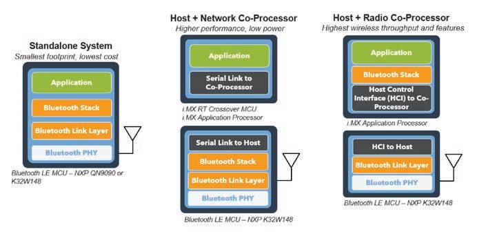
For systems using a high-performance applications processor, the Bluetooth protocol can be cleanly split between the link layer and the stack, with the Bluetooth MCU running only the link layer. This split, and the required Bluetooth stack, are standard in most Linux distributions, making it easier to implement. Many processor providers, including NXP, offer software and products for all three configurations, opening Bluetooth connectivity to a broad range of end device types.

With a smartphone in every pocket, adding Bluetooth connectivity to a standalone end device opens the door to a rich graphical user interface through a smartphone app. No longer specialty devices, modern Bluetooth MCUs are more capable and easier to use than ever before. NXP’s latest K32W148 Bluetooth MCU, for instance, offers 96 MHz of performance, over 1 MB of flash, and advanced security features, all while minimizing power consumption.
Bluetooth MCUs like this offer the ability to add wireless and upgrade the entire end device with more speed, capability, and security. End device designers can easily upgrade their products by replacing buttons and the venerable seven-segment display with Bluetooth and a smartphone app. This, in turn, leads to happier users, better online reviews, and, ultimately, more sales.
Charlie Ice is a Wireless Product Marketer at NXP focusing on the company’s wireless MCUs. He joined NXP in 2022 with more than 10 years of experience managing products in the technology industry. His experience includes microcontrollers, digital motor control, digital power supply control, and test and measurement equipment. Prior to joining NXP, Charlie managed Silicon Labs automotive isolation products. He holds a master’s and B.S. in electrical engineering from Rice University.

“TODAY’S BLUETOOTH MICROCONTROLLERS AND THE BLUETOOTH STANDARD HAVE MADE TREMENDOUS STRIDES IN REDUCING COSTS, COMPLEXITY, AND POWER CONSUMPTION. FIRST, BLUETOOTH HAS EVOLVED THROUGH THE BLUETOOTH LE STANDARD, WHICH MAKES MANY IMPROVEMENTS OVER BLUETOOTH CLASSIC.”

What major trends do you foresee in the module industry for 2024?
With technologies such as artificial intelligence, machine learning/deep learning and 5G being implemented in a rapidly growing number of applications, we are seeing an accelerating increase in data collection. Kontron’s customers span a diverse range of applications from robotic surgery to autonomous vehicles and rugged computers for extreme conditions. We are also seeing most of our customers requiring much higher computing power, larger memory capacity and greater connectivity.
Another trend in the last couple of years is a significant demand for end-to-end solutions combining hardware and software for IoT edge. With an ever-increasing number of devices connected to the internet, there are exponential amounts of data generated from different sensors and devices. More of this data is being processed at the edge with applications such as vision inspection of production lines and autonomous vehicles.
How is Kontron preparing to meet these evolving demands?
To meet these evolving demands, we have set up a working group in the PICMG® standardization committee, together with other leading manufacturers in the industry. The working group has developed a new module standard for High-performance Computing–COM-HPC®
COM-HPC ® expands our already comprehensive portfolio and bridges the gap between our COM Express® modules and our motherboard products. The larger footprint of COM HPC ® allows us to offer products with up to 512GB DDR4 memory, and 20 cores. COM-HPC® also supports the next generation of high-speed interfaces needed for edge devices. Kontron offers credit card-sized modules using low power, such as the COM Express Mini, up to COM-HPC® Server Class modules scalable up to 120 W TDB. Many of these products are also available in extended temperature version, providing great options for harsh environments.
With our numerous offerings, Kontron is well-suited to provide new solutions for embedded hardware for any kind of application.

The performance and lower power of current-generation processors have resulted in single board computers and motherboards being deployed in many products previously requiring highly specialized hardware. Modern embedded systems require a broad range of needs, including high-speed peripherals, networking and a secure platform. Expansion cards to support GPUs, frame grabbers, or other specialized functions often need to be added to increase the system’s functionality. These requirements and more are available in cost-efficient embedded boards from Kontron.
Kontron has long been known as a market leader in COM Express® modules, including the newest generation COM-HPC® form factor. Kontron also has a diverse range of board-level products used in both standalone scenarios and system-level products. Form factors from 3.5" single board computers and mini-ITX to ITX to full ATX server class motherboards are all part of Kontron’s product portfolio. Trade Agreements Act (TAA) compliance is being requested increasingly, and Kontron’s board products are all designed and manufactured in TAAcompliant countries.
Kontron’s diverse range of embedded form factors with embedded computing solutions with performance from Intel Atom class to high core count server-class processors in various markets, including industrial, medical and defense. Another key factor in embedded solutions is long life cycles. Kontron typically provides 7+ years of availability on board-level products, alleviating costly redesigns and/or recertifications triggered by frequent or unexpected EOLs. Demanding environments require high reliability, and Kontron’s focus on 24/7 operation ensures minimal maintenance costs.
The future of embedded boards is quite bright, and Kontron is well-positioned to support the diverse needs of this everexpanding market with Kontron’s diverse portfolio of boards and systems.
Artificial Intelligence has been enjoying another media resurgence since ChatGPT hit the scene earlier this year. ChatGPT is seemingly part of everyone’s vocabulary these days, and its popularity isn’t confined to our consumer lives.
Countless companies have been introducing ChatGPT into their products and product lifecycle. Microsoft uses the same large language models (LLMs) that power the ChatGPT chatbot to power its Bing search engine, and UK-based energy supplier Octopus Energy has built ChatGPT into its customer service channels, with it now responsible for handling 44 percent of customer inquiries.
Generative AI engines, such as GPT-4 that powers ChatGPT, hold enormous potential for insight and innovation around how products are designed and used by customers. But it also raises a few risks and legal questions, venturing into grey areas that have yet to be addressed.

ChatGPT is an advanced language model that uses artificial intelligence (AI) and natural language processing (NLP) to provide conversational responses to users. It’s trained on massive amounts of text data, enabling it to understand and generate human-like language.
For manufacturers, this can be a golden opportunity. Manufacturing companies generate their own specific data from customer usage and equipment performance, and it’s all unique to them. Until now, there have been limits on how companies can monetize and apply this data for development and innovation.
ChatGPT opens the door to accelerate and extend the application of this data. It has the potential to enable design engineers to gain much deeper insights into how the products they design are being used, how they perform over time, and what trends arise, ultimately enabling them to design better products going forward.
ChatGPT can expose manufacturers to additional data so they can uncover, analyze, and harness opportunities they wouldn’t have otherwise spotted. Say, for example, customers are routinely researching what eBike will fit into the back of a Toyota 4Runner. Toyota could capitalize on this and factor it into the future design spec of its next model. Think of ChatGPT as an incredibly efficient assistant. It shouldn’t have the final decision, but it can gather all sorts of information so that you and your designers can make a more informed one.
ChatGPT could also reshape service operations as it matures and moves deeper into day-to-day service and maintenance interactions. Service technicians can use it to ask niche questions they may not know the answer to without having to refer to a manufacturer’s product manual for a complex piece of equipment operating in a specific context.
Likewise, the language comprehension in ChatGPT means service technicians can also provide basic information and use ChatGPT to generate a report, saving time and minimizing the drudge work. Such content generation could eventually be used for customer-facing content, as well as educational, upselling, and personalized cross-selling content.
It also has the potential to triage service maintenance calls and provide more self-service opportunities, helping with costs, unnecessary truck rolls, and sustainability. Furthermore, as older, more experienced technicians retire, ChatGPT can fill the knowledge void, becoming a subject matter expert and providing knowledge guidance either onsite or remotely. With a lack of incoming technicians and growing skills gap, ChatGPT could help alleviate some of the challenges manufacturers face since it can take years to not only understand how to operate the machines, but to also deal with the technicalities of complex modern equipment.
ChatGPT is a tool that can assist engineers in their work, however, it’s not a substitute for the knowledge, expertise,
and creativity that engineers bring to the design and product development process. The AI tool can generate responses for engineering calculations or answer questions about generic engineering knowledge, but those responses should be met with a healthy dose of skepticism and fact checking.
For example, when asked about the best failure theory for ductile materials, ChatGPT gives a thorough explainer of the von Mises yield criterion. But when asked to calculate the moment of inertia on a beam under set conditions, its answer is not in agreement with established values for the moment of inertia about the X-X axis.
Engineers will continue to play a vital role in the design and development of new products and will need to develop new skills and ways of working that enable them to leverage the power of AI tools while also maintaining their unique value as problemsolvers and innovators.

Of course, no tool is perfect. ChatGPT is limited by the quality of the data it’s trained on. While the model is trained on a vast amount of text data, this data is not always representative of real-world language use. The training data may be biased towards certain topics or demographics, leading to limitations in the model’s ability to understand other contexts. Additionally, the data may contain errors or inconsistencies that can impact the model’s performance.
ChatGPT is also limited by the complexity of language. While the model can generate responses to a wide range of questions and prompts, it’s not always able to understand the nuances of language use. This can lead to misunderstandings or incomplete responses. The software may also struggle to understand idiomatic expressions or sarcasm, leading to responses that are not appropriate or relevant.
The newness also carries an element of risk. While ChatGPT version 4 is better than version 3.5, it can still confidently give wrong answers. That’s no different from humans. We do this all the time. But unlike humans, its ability and speed to consume and learn is compounding at a rate faster and deeper than anything a human brain can do. In this sense, risks around ignorance will dramatically decline.
The other potential gray area is that there’s very little legal precedent for the content it is generating. Since ChatGPT pulls content from lots of disparate places and sources, do you 100% own that content? If you use the content and monetize it in some way, who else has a legal claim to it? In time, as generative AI becomes more pervasive and ChatGPT moves into the enterprise, we’ll start to see legal challenges, precedents, and clarity around protection on how ChatGPT creates code, content, and ideas.
What began as a slow creep of AI automation to make things faster is now rapidly accelerating into a mass tipping point of generative intelligence. It’s just a matter of time before AI technology such as ChatGPT is woven into daily business tools, processes, operations, and field support. While the bones of your business may not change, the intelligence, design efficiency, product outcomes, and innovation will almost certainly improve.
Joseph June is the Senior Vice President of Product Management at PTC, a PTC Technology. He has experience with mobile applications, enterprise mobility, enterprise content management, professional services, enterprise software, social media integration, business development, SaaS, cloud computing, and enterprise architecture.
 By Chad Cox, Production Editor
Hackers are looking to rise to that top echelon of attacks, achieving that single intrusion they can brag about for years. One of these hacks worth bragging about is to obtain undetected access to code executed on a programmable logic controller (PLC). Why? Because these systems have an abundance of in-memory protections needing to be bypassed. If successful, the integrated code would be in the thick of existing code going undetected by operating systems or security software. Previous work has required physical access and connections to the PLC, or techniques that target engineering workstations and other links to the PLC in order to gain that level of code execution.
Team82 identified a critical memory security detour vulnerability, CVE-202015782, within Siemens PLCs, the SIMATIC S7-1200 and S7-1500. The common vulnerability and exposure (CVE) disables access protection allowing read and write code everywhere on the PLC or the ability to remotely execute malicious code.
The disclosed vulnerability slides around security within the PLC’s execution ecosystem, as well as a sandbox where code would generally function. Team82 leveraged CVE-2020-15782, evading the sandbox to access memory for writing and infusing shellcode to attack the Siemens 1200/1500 PLCs. To “jailbreak” the native SIMATIC S7-1200 and S7-1500 sandboxes, Team82 utilized its memory protection bypass vulnerability, allowing the black-hats to input random data to “protected” memory or read critical information for further exploitations of the environment.
The Siemens S7 PLCs are powered by the ADONIS kernel and an ARM or MIPS core. The controller is compatible with many programming languages including Structured Control Language (SCL), Ladder Diagram (LD), Statement List (STL), and Function Block Diagram (FBD).
Claroty had to reverse engineer the bytecode language (Siemens has yet to publicly disclose information on how to decode the MC7/MC7+ bytecode) to learn more about the internal environment and to find areas to exploit.
Team82’s virtual machine hinders data flow in user’s programs with compiled bytecode made available by the operating system and not direct hardware operation. This constrains the user and code to a specific protocol deemed safe*, locking code into the sandbox with reduced access to storage and resources, and crippling functionality, thereby damaging the PLC.
Team82 summarizes, “Escaping the sandbox means an attacker would be able to read and write from anywhere on the PLC, and could patch an existing VM opcode in memory with malicious code to root the device. Claroty, for example, was able to inject ARM or MIPS shellcode directly to an internal operating system structure in such a way that when the operating system uses a specific opcode that we chose, our malicious shellcode would execute, giving us remote code execution. We used this technique to install a kernel-level program with some functionality that is completely hidden to the operating system.”
› CVE-2020-15782
› CWE-119 Improper Restriction of Operations within the Bounds of a Memory Buffer
› CVSS v3.1 Score: 8.1
*For example, the operating system will restrict any direct access to protected memory, but will allow the use of any function from the standard library provided by Siemens (e.g. ADD_I - Add Integer subroutine).
In the rapidly changing technology universe, embedded designers might be looking for an elusive component to eliminate noise, or they might want low-cost debugging tools to reduce the hours spent locating that last software bug. Embedded design is all about defining and controlling these details sufficiently to produce the desired result within budget and on schedule.
Embedded Computing Design (ECD) is the go-to, trusted property for information regarding embedded design and development. embedded-computing.com


eDNP/8331: Virtual SoM with Embedded Debian Linux O/S
The eDNP/8331 is a 32-bit Arm-based virtual Systemon-Module (SoM) including Debian Linux operating system and firmware functions for headless embedded gateways that is available as intellectual property under a licensing model. The entire SoM hardware is supplied as schematic and PCB snippet for the widely used PCB development environment "Altium Designer". This enables the development and production of own assemblies with seamlessly embedded SoM functions or application-specific SoM devices with special pinouts and form factors.
Various function extensions are available via a library. These include, for example, a second 10/100 Mbps Ethernet LAN interface, Bluetooth, Wi-Fi, NB-IoT, LTE-M, LTE-A, etc., as well as cryptographic secure elements for a HWbased PKI.
The pre-engineered combination of HW and SW building blocks makes the eDNP/8331 particularly suitable for embedded IoT gateways, OT/IT integration gateways, X.509 PKI-based VPN endpoints, IIoT multi-factor authentication (MFA) solutions, and highly secure end-to-end data applications with digital signatures.
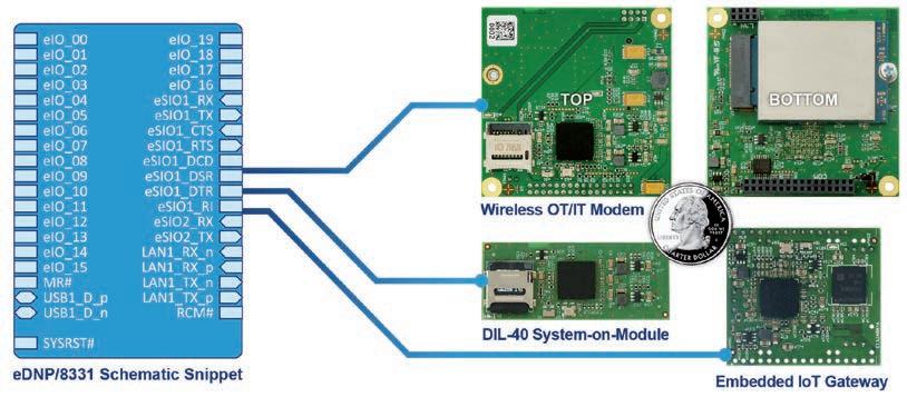
Ą CAD data for HW function + customized open source SW
Ą Project integration via Altium schematic/PCB snippet
Ą Bootable image with U-Boot, Debian Linux O/S and UI
Ą Firmware functions for embedded gateway applications
Ą HW/SW prebuild for Arm-based Allwinner/Sochip S3 SoC
Ą Various NAND flash versions (e.g. SD card, eMMC)
Ą Numerous HW/SW functions for circuit extensions
Ą Python runtime environment with OTA software updates
Ą Mass production Flash programming support for eMMC
Ą Hardware mass production support (e.g. AOI, MOI, ICT)
Ą Migration concept for HW-independent applications
Ą Customization support for various SoCs, I/O functions and Linux driver integration available
The UDE Universal Debug Engine is the perfect tool for runtime analysis and testing of embedded multicore applications. With support for on-chip tracing, it offers comprehensive features for non-intrusive debugging, runtime observation, and runtime measurement. This helps developers to investigate, e.g., timing problems or misbehavior caused by parallel execution.
Used in conjunction with the UAD2next and UAD3+ devices from the Universal Access Device family, the UDE enables trace data to be captured from various trace sources and via external trace interfaces. Trace modules for the UAD2next or trace pods for the UAD3+ are provided for this purpose.
UDE's debugging and tracing capabilities, coupled with a flexible and open API for scripting and integrating with third-party tools, make UDE an ideal choice for automated testing on real target hardware. During the execution of automated tests, UDE can also determine the Code Coverage to validate the quality of the test cases that are being used.
UDE Universal Debug Engine for Multicore Debugging is a powerful development platform for debugging, testing and system analysis of microcontroller software applications. UDE enables efficient and convenient control and monitoring of multiple cores for a wide range of multicore architectures within a single common user interface. This makes it easy to manage even complex heterogeneous multicore systems.
UDE supports a variety of multicore microcontrollers and embedded multicore processors including Infineon AURIX, NXP S32 Automotive Platform, STMicroelectronics Stellar, Renesas RH850, Synopsys ARC, RISC-V and others.
The UAD2pro, UAD2next and UAD3+ devices of the Universal Access Device family provide the hardware basis for the powerful functions of UDE and enable efficient and robust communication with the supported architectures and controllers. With its flexible adapter concept, the Universal Access Device family supports all commonly used debug interfaces.
Ą Visualization and analysis of recorded trace information (execution sequence chart, call graph visualization, profiling)
Ą Trace-based, non-intrusive statement coverage (C0 coverage) and branch coverage (C1 coverage) for proving test quality
Ą Open and flexible software API for scripting and test automation


Ą Debugging of homogeneous and heterogeneous 32-bit and 64-bit multicore MCUs and embedded MPUs
Ą Synchronous break, single step and restart for multicore systems
Ą One common debug session for complete system / all cores
Ą Convenient debugger user interfaces supporting multi-screen operation and perspectives
Ą Support for special cores including GTM, HSM, PPU, SCR
Ą Software API for tool automation and scripting
Ą AUTOSAR support and RTOS awareness
34 Embedded Computing Design RESOURCE GUIDE | Fall 2022 www.embeddedcomputing.com
ASUS IoT edge AI systems combine GPU computing with AIoT potential. They offer embedded MXM GPU modules from both NVIDIA® and Intel®, NVIDIA® Jetson-based platforms, and GPU computing platforms for diverse market needs. With unparalleled performance, they enable realtime AI inferencing at the edge, transforming industries.
Designed with a rugged, fanless, anti-vibration build, wide temperature support and low power consumption, they excel in demanding edge AI applications like factory automation, machine vision, video analytics, and autonomous vehicles.
ASUS IoT ensures robustness and reliability for the most challenging scenarios, driving innovation and efficiency in this new era.
Ą Powerful & Scalable GPU Computing: ASUS IoT pioneers the industry's first edge AI system that supports up to dual 450-watt TDP GPUs. ASUS IoT systems benefit from support for Intel Arc™ A-series MXM, NVIDIA PCIe® GPU cards, and Jetson SoM, offering a choice of power-efficient options through to extreme high-throughput solutions.
Ą Latest Computing Platform: ASUS IoT edge AI systems are available in a variety of form factors embedded with the latest Intel 13th/12th Gen CPUs and NVIDIA Jetson Orin™ series, meeting the dynamic requirements of the market.
Ą Exclusive Thermal Design: The patented system design effectively diffuses heat from the CPU, GPU, and all peripherals, delivering extreme ruggedness with a fanless structure. This ensures stable operation while the fanless design further reduces dust generation and thus enhances durability.
Ą Robust Power Design: Innovative high-current tolerance power design ensures extreme reliability under a wide range of DC inputs and power-hungry GPU computing. Support for ignition power control adds further stability.
Ą Anti-vibration Design: With a robust mechanical design featuring structured support, GPU retainer, cable screw lock, and damping bracket, ASUS IoT edge AI systems excel at in-vehicle situations for smooth and uninterrupted operation.
Ą Industrial Feature Set & Rich I/O: Supports PoE, isolated DIO, multiple COM ports, CAN bus, and more, enabling seamless connectivity for a wide range of applications.

Ą Certification Compliance: Rest assured with our system-validated certification readiness. Our edge AI systems comply with MIL-STD 810H and offer vibration resistance up to 5 GRMS.
Ą Software Support for Easy Integration: Simplify the integration process with comprehensive software support, including APIs, middleware, and device control toolkits tailored for various vertical applications.
https://www.asus.com/content/asus-iot-edge-ai-systems

With 40+ years of expertise in edge computing design, system assembly, custom packaged product, and IoT software platforms, SECO enables its customers with end-to-end solutions, from edge device hardware to fully integrated products with Artificial Intelligence (AI) technologies that transform businesses.

Edge Computing
SECO provides a broad array of cutting-edge embedded computing building blocks through worldwide engineering design, manufacturing, and technical support excellence.
Off-the-shelf computer-on-module (COM) and single board computer (SBC) products feature leading processing technologies (NXP, Intel®, MediaTek, Xilinx, AMD) compliant with major standards (SMARC, QSeven®, COM-HPC®, COM Express®, Pico-ITX, eNuc). Modular HMIs, rugged tablets, fanless PCs, and communication gateways complete SECO’s off-the-shelf edge portfolio. SECO also offers custom design and integration of electronic devices.
Featured Products
• Qseven®: choose from NXP i.MX 8M Mini and Nano, i.MX 8X, i.MX 8 Arm® application processors, and Intel® Atom® X6000E series (formerly Elkhart Lake) for AIoT applications.
• SMARC: processors include NXP i.MX 8M Plus, i.MX 8X, and i.MX 93, MediaTek Genio 700 Arm®, and Intel® Atom® X6000E series (formerly Elkhart Lake) for connected multimedia.
• COM-HPC® Client Size A: offering 11th Gen Intel Core™ (formerly Tiger Lake-UP3), Xeon® W-11000E Series (formerly Tiger Lake-H), and 12th Gen Intel Core™ (formerly Alder Lake – H series) processors, for high end automation and AI at-the-edge.
• COM Express® Type 6: pick your performance from Intel® Atom® X6000E series (formerly Elkhart Lake), 11th Gen Intel® Core™ (formerly Tiger Lake UP3), and 13th Gen Intel® Core™ processors (formerly Raptor Lake-P) - for graphic edge applications.
CLEA is SECO’s IoT software suite that easily connects edge electronic devices (SECO-based hardware and others) to the cloud and facilitates real time device monitoring, analytics, infrastructure management, predictive maintenance, secure remote software updates, data orchestration, and more. Optimize and grow your business through smart use of real time data.
StudioX is a novel AI-driven platform for intelligent streamlining of business operation processes, product offerings, and customer service. Trained on existing company documents and data, and learning on-the-fly, StudioX leverages institutional knowledge to resolve complex problems quickly, communicates with natural language, and frees employees for higher value tasks.
Ą Off-the-shelf embedded products: SOMs, SBCs, HMI devices, and gateways compliant with widely used standards.
Ą Operating systems for edge devices: Linux, Android, Windows, and RTOS such as VxWorks modified to match edge device hardware.
Ą Customized computing platforms: custom-designed circuitry, software, and enclosures to meet unique product requirements.
Ą CLEA: software suite solution that integrates IoT, cloud computing, and big data analysis for easy deployment and facilitates efficient distributed operations.
Ą StudioX: AI-driven software platform that smartly combines organizational knowledge with smart apps that optimize your process, products, and services.
Ą Embedded AI: algorithms that autonomously analyze and optimize operation on the edge device without cloud connectivity.
Ą Product development: design and production of rugged high reliability electronic devices, including rugged tablets, handheld controllers, medical devices, and industrial equipment.
Ą World-class electronics manufacturing: ISO 9001 and 13485.
Ą US-based engineering and operations: for direct support of North America clients.
The SI-624-AI is an industrial AI computer designed to meet the demands of high-speed multiple tasks for AI deep learning. Powered by the 12th Gen Intel® Core™ CPU and incorporating the NVIDIA Ampere Architecture MXM GPU, the system delivers image processing capabilities that enable real-time analysis of visual data, enhancing automation, quality control, and overall production efficiency for AIoT applications in smart factory, retail, transportation or medical fields. It is suitable for use as a digital signage control system in missioncritical control rooms in transportation networks, smart retail, or healthcare where remote AI data analysis capabilities are required.
FEATURES
2x DDR4-3200 SO-DIMM, Max. 64GB, ECC compatible
iSMART intelligent energy-saving & Observer remote monitoring technologies

4x DP++ output
1x M.2 B-Key (3052) for 5G or LTE options, 1x M.2 E-Key (2230) & 2x M.2 M-Key (2280) for Wi-Fi, Bluetooth, capture or storage options
Supports OOB function via I210 LAN port (optional), TPM 2.0
SI-624-AI www.ibase.com.tw/en/product/category/Intelligent_System/Industrial_AI_Computer/AI_Accelerator_Compatible_Computer/SI-624-AI

The TS-4900 is a high-performance TS-SOCKET System on Module based on the NXP i.MX6 CPU which implements the Arm® Cortex®-A9 architecture clocked at 1 GHz (Single or Quad Core) and paired with 1GB or 2GB of DDR3 RAM.
Several industry-standard interfaces and connections such as Gigabit Ethernet, WiFi and Bluetooth, USB, SATA II, PCI Express, and more make the TS-4900 a great fit for nearly any embedded systems application, especially those needing wireless connections like industrial internet of things (IIOT) gateway.
1 GHz Single or Quad Core Cortex-A9 Arm CPU
2 GB DDR3 RAM
4GB MLC eMMC flash storage
Up to 70x DIO, 2x I2C, 1x I2S, 2x SPI, 2x CAN
Industrial temperature range (-40°C to 85°C)
www.embeddedcomputing.com Embedded Computing Design RESOURCE GUIDE | Fall 2023 37

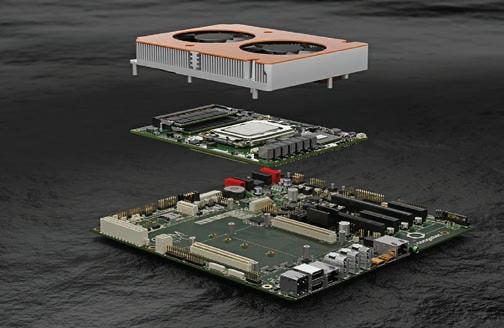
The new conga-HPC/uATX industrial-grade COM-HPC carrier board in Micro-ATX form factor is designed for embedded longterm availability of at least seven years, which eliminates the design risks, revision requirements and supply chain uncertainties of standard or semi-industrial-grade motherboards that are usually only deliverable for three to five years. As it is processor socket and vendor independent, the board can be equipped with any high-end Computer-on-Module available in COM-HPC Client Size A, B or C, making OEM designs even more flexible and sustainable. Impressive scalability across the entire range of 12th Generation Intel Core processor-based COM-HPC modules. Performance options for the new conga-HPC/uATX carrier board range from the conga-HPC/cALS COM-HPC Client Size C modules, offering the currently highest embedded client performance with 16-core Intel Core i9 processor, to the masters of price/ performance optimization – the conga-HPC/cALP COM-HPC
Client Size A modules with Intel Celeron 7305E processor.
The combination of application-ready industrial-grade COMs & carrier boards with tailored cooling solutions and comprehensive BSPs for all leading RTOSes and the real-time hypervisor from Real-Time Systems is perfect for fastest time-to-market, produces lowest non-recurring engineering costs, enables customers to react very quickly to changing market requirements and reduces the effort to scale the performance of Micro-ATX based systems to a minimum. It allows customers to create a full product portfolio based on one single carrier concept.
The carrier board offers the latest interface enhancements such as PCIe Gen4 and USB 4 and is a perfect fit for system designs with congatec’s latest high-end COM-HPC Client modules based on the 12th generation Intel Core i9/7/5/3 desktop processors (formerly code-named Alder Lake-S). Most impressive is the fact that engineers can now leverage Intel’s innovative performance hybrid architecture. Offering of up to 16 cores/24 threads, 12th Gen Intel Core processors provide a quantum leap in multitasking and scalability levels.
Next-gen IoT and edge applications benefit from up to 8 optimized Performance-cores (P-cores) plus up to 8 low power Efficient-cores (E-cores) and DDR5 memory support to accelerate multithreaded applications and execute background tasks more
efficiently. Optimized for highest embedded client performance, the graphics of the LGA processor based modules delivers now up to 94% faster performance and its image classification inference performance has nearly tripled with up to 181% higher throughput. In addition, the modules offer massive bandwidth to connect discrete GPUs for maximum graphics and GPGPU based AI performance.
Ą Application Carrier Board for COM-HPC Client Type Modules (Sizes A, B, C) in Micro-ATX form factor. Size 244 x 244 mm2
Ą Besides highest bandwidth and performance, the new flagship COM-HPC Client modules impress with dedicated AI engines supporting Windows ML, Intel Distribution of OpenVINO toolkit and Chrome Cross ML
Ą Different AI workloads can seamlessly be delegated to the P-cores, E-cores, as well as the GPU execution units to process even the most intensive edge AI workloads
Ą The built-in Intel Deep Learning boost technology leverages different cores via Vector Neural Network Instructions (VNNI), and the integrated graphics supports AI accelerated DP4a GPU instructions that can even be scaled to dedicated GPUs
Ą Intel’s lowest power built-in AI accelerator, the Intel Gaussian & Neural Accelerator 3.0 (Intel GNA 3.0), enables dynamic noise suppression and speech recognition and can even run while the processor is in low power states for wake-up voice commands.
embeddedTS is proud to introduce the TS-7100-Z, our smallest single board computer in an optional DIN-mountable enclosure that measures 2.4" by 3.6" by 1.7", powered by the Arm® Cortex®-A7 based iMX6 UltraLite CPU. It ships with industry-standard interfaces, including Ethernet, USB, RS-232, RS-485, and CAN.
For wireless connectivity, the TS-7100-Z comes with WiFi and Bluetooth module, as well as a NimbeLink/Digi cellular modem and mesh network socket. With all of these features packed into a smaller footprint, not only will the TS-7100-Z fit in your cabinet, but it can also help to replace other peripherals and modules to free up even more space and get more done. Combining all of these components into one small DIN-mounted unit, we provide the ability to promote hot swapping in the field, limiting costly technician time and troubleshooting.
embeddedTS
www.embeddedTS.com
Ą NXP i.MX 6UltraLite 696 MHz Arm® Cortex®-A7
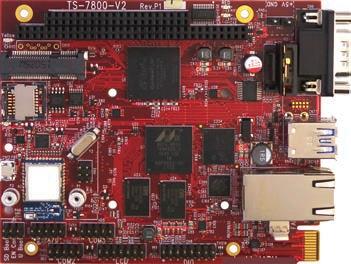
Ą 512 MB RAM
Ą 4 GB eMMC Flash Storage
Ą 2 KB FRAM Storage
Ą 3" 18-bit, 320x240, 135dpi Resistive Touchscreen Display (Optional)
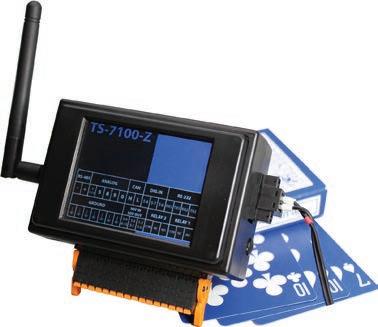
https://www.embeddedts.com/products/ts-7100-Z
sales@embeddedTS.com
@ embeddedTS
480-837-5200
Powered by the Marvell Armada 385 Dual Core 1.3 GHz Arm® Cortex®A9-based CPU, the embeddedTS TS-7800-V2 industrial Single Board Computer (SBC) stands out from the crowd with its high-performance components, connectivity options, and an unbelievable feature set packaged into a small footprint in both size and power. It's a general-purpose, low-power SBC ready to tackle demanding applications, including data acquisition, IoT, industrial automation, or any rugged deployment.
The guaranteed 10+ year lifecycle ensures a long-term deployment in the field, free from expensive replacements that come from short, disposable lifecycles, which are all too common. With the included heat sink, the fanless design of the TS-7800-V2 can withstand high vibration, and even with two CPU cores running at 1GHz and tasked to their max, the system can operate at a wide temperature range of -40 °C to 85 °C.
embeddedTS
www.embeddedTS.com
Ą Marvell Armada 385 Dual Core 1.3 GHz Arm-based CPU
Ą 1 DDR3 RAM
Ą 4 GB MLC eMMC Flash
Ą Flexible Data Storage: eMMC, SATA, mSATA, SD Card or uSD Card Expansion
Ą Easily Interfaces via PC/104, USB 3.0, Gigabit Ethernet, ADC, GPIO and More
https://www.embeddedts.com/products/TS-7800-V2
sales@embeddedTS.com


@ embeddedTS
480-837-5200
The XEM8310-AU25P development module with AMD-Xilinx Artix™ UltraScale+ FPGA offers integrators a turnkey solution with fast (340+ MB/s) USB 3.0 host interface using the Opal Kelly FrontPanel® SDK. Designed for both prototype / proof-of-concept and production deployment, the highly-integrated device includes on-board power supplies, DDR4 memory, and support circuitry in a compact form factor with commercial-off-the-shelf (COTS) availability.
The FrontPanel SDK greatly simplifies hardware / software communication with a comprehensive and easy-to-use API and broad operating system and language support. Opal Kelly SOMs reduce time-to-market, allow teams to focus on their core competencies, and simplify supply chains. Opal Kelly has been ISO 9001:2015 certified since 2019.


Typical applications include:
• ●Data acquisition
• ●Test & measurement, instrumentation, and control
• ●Machine vision / machine learning / AI
• ●Software-defined radio (SDR)
• ●Digital communications and networking
• ●Data security
Development Platform with AMD-Xilinx Artix
UltraScale+ FPGA
The XEM8320-AU25P Development Platform is the official AMD-Xilinx Artix™ UltraScale+ development platform, complete with full support for Opal Kelly's FrontPanel® SDK for high-performance software-connected FPGA applications over USB 3.0. A complete line of SYZYGY® peripherals provide data acquisition, video capture, networking, and interface solutions in a modular, expandable ecosystem – perfect for lab-born prototypes. Easy transition to proof-of-concept and production is supported by the compact XEM8310 system-on-module.
In addition to 6 SYZYGY® peripheral ports, two SFP+ cages and SMA connectors are available with connections to the FPGA's 16.375-GHz transceivers. Typical applications include:
• ●Data acquisition
• ●Test & measurement, instrumentation, and control
• ●Machine vision / machine learning / AI / MIPI
• ●Software-defined radio (SDR)
• ●Digital communications and networking
• ●Data security
Ą AMD-Xilinx Artix UltraScale+ XCAU25P-2FFVB676E
Ą SuperSpeed USB 3.0 port for high-bandwidth data transfer
Ą 2 GiB DDR4 (32-bit data interface), 32 MiB QSPI FPGA flash
Ą 149 FPGA fabric I/O and 12 gigabit transceiver lanes (16.375 Gbps)
Ą Compact form factor (100mm x 70mm)
Ą Full FrontPanel SDK and API support
https://opalkelly.com/products/xem8310/
Ą AMD-Xilinx Artix UltraScale+ XCAU25P-2FFVB676E
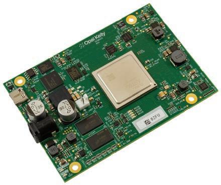
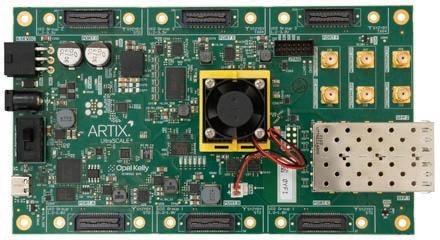
Ą SuperSpeed USB 3.0 port for high-bandwidth data transfer
Ą 1 GiB DDR4 (16-bit data interface)
Ą 4x SYZYGY Standard peripheral ports
Ą 2x SYZYGY Transceiver peripheral ports
Ą 2x SFP+ transceiver sockets
Ą Full FrontPanel SDK and API support
https://opalkelly.com/products/xem8320/
VME and VME64x, CompactPCI, or PXI chassis are available in many configurations from 1U to 12U, 2 to 21 slots, with many power options up to 1,200 watts. Dual hot-swap is available in AC or DC versions. We have in-house design, manufacturing capabilities, and in-process controls. All Vector chassis and backplanes are manufactured in the USA and are available with custom modifications and the shortest lead times in the industry.
Series 2370 chassis offer the lowest profile per slot. Cards are inserted horizontally from the front, and 80mm rear I/O backplane slot configuration is also available. Chassis are available from 1U, 2 slots up to 7U, 12 slots for VME, CompactPCI, or PXI. All chassis are IEEE 1101.10/11 compliant with hot-swap, plug-in AC or DC power options.
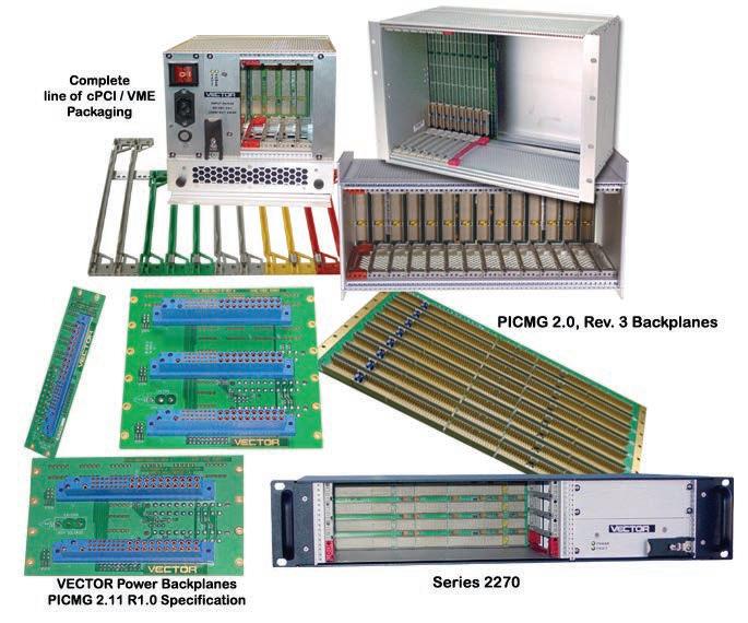
Our Series 400 enclosures feature side-filtered air intake and rear exhaust for up to 21 vertical cards. Options include hot-swap, plug-in AC or DC power, and system voltage/temperature monitor. Embedded power supplies are available up to 1,200 watts.
Series 790 is MIL-STD-461D/E compliant and certified, economical, and lighter weight than most enclosures available today. It is available in 3U, 4U, and 5U models up to 7 horizontal slots.
All Vector chassis are available for custom modification in the shortest time frame. Many factory paint colors are available and can be specified with Federal Standard or RAL numbers.


Ą Most rack accessories ship from stock
Ą Modified ‘standards’ and customization are our specialty
Ą Card sizes from 3U x 160mm to 9U x 400mm
Ą System monitoring option (CMM)
Ą AC or DC power input
Ą Power options up to 1,200 watts
For more detailed product information, please visit www.vectorelect.com or call 1-800-423-5659 and discuss your application with a Vector representative.
Introducing the COMe-mRP10 (E2). Based on the 13th Gen Intel® Core™, it provides a considerable performance increase compared to the past generation. The COM-Express® module comes with 14 cores originating from Intel® performance hybrid architecture and offers essential, industrial-grade attributes for embedded systems in demanding areas.
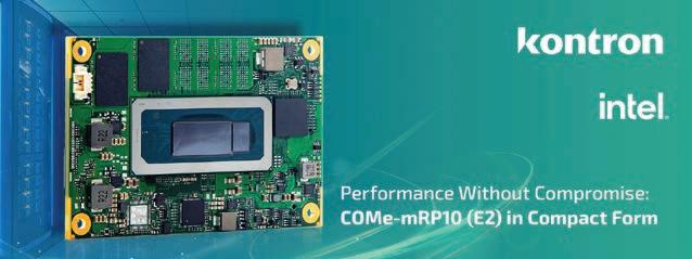
Ą High-Performance Processors: Built on the foundation of the 13th Gen Intel® Core™ (known formerly as Raptor Lake-P), the 14 cores ensure increased processing capability.
Ą Memory: Supports up to 32 GByte LPDDR5(x) memory down. More memory means multi-tasking and handling data-intensive operations are easier.
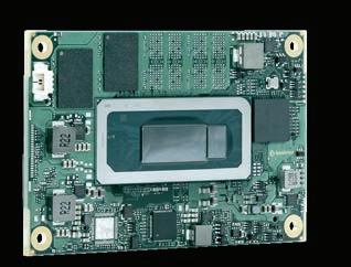
Ą Networking: Offers up to a 2.5 Gb Ethernet connectivity with specialized TSN support, making real-time communication more efficient.
Ą Storage: An optional NVMe SSD onboard ensures faster data access, storage, and retrieval.
Ą Industrial Grade: Keeping the industrial applications in mind, the COMe-mRP10 (E2) is built rugged. It operates effectively in temperatures ranging from -40C to +85C.
Ą Advanced Technology Support:
• In-Band Error Correction Code (IBECC) Memory: Enhances data integrity, ensuring every bit of information is precise and free from errors.
Applications:
The versatility of the COMe-mRP10 (E2) makes it suitable for:
• Industrial Automation: Enhance process efficiencies, control machinery with precision, and optimize operations in real-time.
• Health Care: Whether it’s sophisticated medical equipment or patient management systems, enjoy faster processing and reliable operations.
• Intel® Time Coordinated Computing (Intel® TCC): This feature guarantees precise timing coordination in operations, an essential for several real-time applications.
• Time-Sensitive Networking (TSN): With TSN, real-time networking gets a boost. It ensures timely delivery of data packets, making applications more responsive and reliable.

K9051-C741 ATX
In today’s digital age, where high-performance computing (HPC) is essential for industrial automation, artificial intelligence (AI), data sequencing, and imaging, a powerful server-class motherboard is a crucial component in the market. Created based on industry needs, Kontron introduces its newest motherboard, the K9051-C741 ATX, supporting Intel® 4th/5th Gen Intel® Xeon® scalable processors with up to 64 cores, 768 GByte memory, and multiple expansion options.
The K9051-C741 ATX server-class motherboard with Intel® C741 chipset, comes with five PCIe Gen 5 expansion slots, independent memory channels and supports a broad range of I/O options making it ideal for today’s most demanding applications. The board has eight separate RDIMM sockets supporting a maximum memory density of 768 GBytes at up to 5600 MT/s. This makes the K9051-C741 ATX motherboard well-suited for HPC needs including high core count processors, large memory banks and support for modern data interface requirements.
Kontron’s latest motherboard also features five PCIe slots, including three PCIe Gen5 x16 and two PCIe Gen5 x8, for various expansion cards. Equipped with two 10GBASE-T RJ45 Ethernet ports, it ensures fast and reliable network connectivity. For storage, the K9051-C741 ATX supports up to six SATA 6G and M.2 PCIe/ NVMe connections including support for RAID configurations. In addition, the board supports high-speed peripherals via six USB 3.1 Gen1 ports.
Ą Intel® 4th/5th Generation Xeon® scalable processor

Ą Intel® C741 Chipset
Ą 8x DDR5 5600 MT/s RDIMM Independent Channels
Ą 3x PCIe Gen5 x16 slots and 2 x PCIe Gen5 x8 slots
Ą 2x 10GBASE-T RJ45 Ethernet ports
Ą 6x SATA 6G incl. RAID support
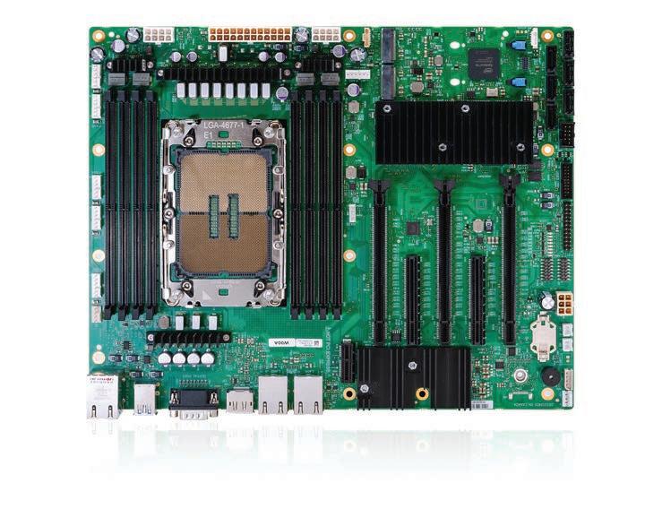
Ą 4x Type A connectors USB 3.2 Gen1 (5Gbps)
Ą DisplayPort connector via AST2600 video output
Ą TPM version 2.0
Ą 10-year extended supply availability
Leveraging multi-decade excellence in design and manufacturing, SECO embedded products feature leading edge processing technologies, based on x86, Arm®, and FPGA architectures from world-class silicon vendors. SECO offers multiple standard form-factor computing platforms in addition to HMIs, fanless PCs, communication gateways, and custom product.
SECO’s SMARC product family offers multiple processor options within a compact Computer-on-Module (COM) standard for products that require high performance and low power usage. Providing a processor, memory, storage, display and Ethernet interfaces, USB, and more, SMARC offers an embedded computing module within a compact 3.23x1.97-inch standard form-factor.
SECO’s SMARC product family offers Arm® (NXP and MediaTek), x86, and FPGA options, with associated Linux, Android, and Windows operating systems.
With client electronic design limited to an application-specific carrier board, SMARC modules merge the ability to withstand rugged environmental conditions with excellent scalability and high configurability. SMARC is the perfect fit for products ranging from industrial IoT to HMI and smart digital signage, to smart city and home automation.
Beyond SMARC modules, SECO wide portfolio of embedded boards also includes many other form factors, including Qseven®, COM Express®, COM-HPC®, and single board computer (SBC).
FEATURES:
Ą Standard form-factor computing engine
Ą Electronics design investment limited to the carrier board
Ą Scalable, future-proof, long-term availability
Ą Arm® (NXP, MediaTek, Xilinx) and x86 (Intel®)
Ą Industrial temperature, conformal coat options
CLEA, a comprehensive IoT platform from SECO, easily connects edge electronic devices to the cloud and facilitates real time device monitoring, analytics, infrastructure management, predictive maintenance, secure remote software updates, and more.

CLEA turns data from connected devices into actionable insights. The platform enables full retrofitting of existing infrastructure, rapid integration, high-performance data orchestration, and quick and easy deployment of AI applications on a mass scale. CLEA scales to large numbers of connected devices – located in multiple locations, across a variety of hardware platforms, performing different functions. Integration with existing infrastructure is simple- improving efficiency, accelerating time to market, and allowing companies to quickly develop products and services with high added value. Bottom line: CLEA significantly improves operational efficiency, ROI, and data monetization.
CLEA is both ready to use and customizable for applications ranging from small installations to large enterprise solutions. Predictive maintenance of machinery, sales trend forecast analysis, monitoring of medical parameters, and optimization of operations are a few examples of the wide variety of CLEA uses. From vending to medical, from factory automation to energy management, CLEA is the one stop solution for deploying industry 4.0 quickly and economically, unlocking new business opportunities and efficiencies.
FEATURES:
Ą Device lifecycle management: CLEA manages OTA updates, remote debugging, blue/green app deployments and much more, with a strong focus on security.
Ą Data orchestration: CLEA easily scales to large numbers of connected devices and exchanged messages. Configure and customize your data journey optimally for your business.
Ą Deploy AI models and smart apps: as a distributed data management platform, CLEA enables you to easily deploy data driven intelligence at the edge or in the cloud, seamlessly.
Ą Rich, featureful APIs: everything in CLEA is API based, both at the edge and in the cloud. You are in full control and can easily add new capabilities.
Ą Open-source core: all core middleware CLEA components are open-source software.

Ą No lock-in with SECO. You own your data. Deploy your own cloud or leverage SECO’s.

Lauterbach ARMv8 support at a glance: More than 17 years of experience in ARM debugging enable Lauterbach to provide best-in-class debug and trace tools for ARMv8 based systems:
• Multicore debugging and tracing for any mix of ARM and DSP cores
• Support for all CoreSight components to debug and trace an entire SoC
• Powerful code coverage and run-time analysis of functions and tasks
• OS-aware debugging of kernel, libraries, tasks of all commonly used OSs
Lauterbach debug tools for ARMv8 help developers throughout the whole development process, from the early pre-silicon phase by debugging on an instruction set simulator or a virtual prototype over board bring-up to quality and maintenance work on the final product.
Debugger features range from simple step/go/break, programming of on-chip-flash, external NAND, eMMC, parallel and serial NOR flash devices and support for NEON and VFP units, to OS-aware debug and trace concepts for 32-bit and 64-bit multicore systems.
TRACE32 debuggers support simultaneous debugging and tracing of homogeneous multicore and multiprocessor systems with one debug tool.
Start/Stop synchronization of all cores and a time-correlated display of code execution and data r/w information provides the developer with a global view of the system's state and the interplay of the cores.
Ą Full support for all CoreSight components
Ą Full architectural debug support
Ą Support for 64-bit instruction set and 32-bit instruction sets ARM and THUMB
Ą 32-bit and 64-bit peripherals displayed on logical level
Ą Support for 32-bit and 64-bit MMU formats
Ą Auto-adaption of all display windows to AArch32/ AArch64 mode
Ą Ready-to-run FLASH programming scripts
Ą Multicore debugging
Ą On-chip trace support (ETB, ETF, ETR)
Ą Off-chip trace tools (ETMv4)
Ą AMP debugging with DSPs, GPUs and other accelerator cores
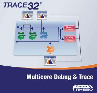
Lauterbach TriCore debug support at a glance:
For more than 15 years Lauterbach has been supporting the latest TriCore microcontrollers. Our tool chain offers:
• Single and multicore debugging for up to 6 TriCore cores
• Debugging of all auxiliary controllers such as GTM, SCR, HSM and PCP
• Multicore tracing via MCDS on-chip trace or via high-speed serial AGBT interface
The Lauterbach Debugger for TriCore provides high-speed access to the target application via the JTAG or DAP protocol. Debug features range from simple Step/Go/Break up to AutoSAR OS-aware debugging. High speed flash programming performance of up to 340kB/sec on TriCore devices and intuitive access to all peripheral modules are included.
Lauterbach’s TRACE32 debugger allows concurrent debugging of all TriCore cores.
• Cores can be started and stopped synchronously.
• The state of all cores can be displayed side by side.
• All cores can be controlled by a single script.
Ą Debugging of all auxiliary controllers: PCP, GTM, HSM and SCR
Ą Debug Access via JTAG and DAP
Ą AGBT High-speed serial trace for Emulation Devices
Ą On-chip trace for Emulation Devices
Ą Debug and trace through Reset
Ą Multicore debugging and tracing
Ą Cache analysis
Lauterbach RH850 debug support at a glance:
The Lauterbach Debugger for RH850 provides high-speed access to the target processor via the JTAG/LPD4/LPD1 interface. Debugging features range from simple Step/Go/Break to multicore debugging. Customers value the performance of high-speed flash programming and intuitive access to all of the peripheral modules.
TRACE32 allows concurrent debugging of all RH850 cores.
• The cores can be started and stopped synchronously.
• The state of all cores can be displayed side by side.
• All cores can be controlled by a single script.
All RH850 emulation devices include a Nexus trace module, which enables multicore tracing of program flow and data transactions. Depending on the device, trace data is routed to one of the following destinations:
• An on-chip trace buffer (typically 32KB)
• An off-chip parallel Nexus port for program flow and data tracing
• A high bandwidth off-chip Aurora Nexus port for extensive data tracing
The off-chip trace solutions can store up to 4GB of trace data and also provide the ability to stream the data to the host for long-term tracing, thus enabling effortless performance profiling and qualification (e.g. code coverage).
Ą AMP and SMP debugging for RH850, GTM and ICU-M cores
Ą Multicore tracing
Ą On-chip and off-chip trace support
Ą Statistical performance analysis
Ą Non intrusive trace based performance analysis
Ą Full support for all on-chip breakpoints and trigger features
Ą AUTOSAR debugging
PX5 enhances, simplifies, and unites embedded development. We deliver on this mission with superior products, an expert team, and a focus on supporting you throughout your development effort. Our team of engineers have extensive embedded experience (previously authored ThreadX and Nucleus RTOS products). Our products, support and vast experience will help you deliver higher quality, safer, and more secure products to market in less time and with lower cost. When you succeed, we succeed!
The PX5 RTOS is ULTRASMALL (< 1KB of FLASH and 1KB of RAM for minimal use), enabling its use in the most memory-constrained devices. It’s ULTRAHIGH PERFORMANCE (sub-microsecond context switching and API calls on most microprocessors) and rich determinism make it ideal for the most demanding real-time needs.
PX5 RTOS also boasts best-in-class SAFETY AND SECURITY. The entire PX5 RTOS code base is rigorously tested – 100% C statement and branch decision coverage testing for every release. In addition, the PX5 RTOS also offers patent-pending Pointer/Data Verification (PDV) technology, a unique way to provide unprecedented run-time function pointer, system object, buffer, and stack verification. Finally, the PX5 RTOS has been functional safety certified for use in devices requiring IEC-61508 SIL 4, IEC-62304 Class C, ISO 26262 ASIL D and EN 50128 SW SIL 4.
The PX5 RTOS is SIMPLE. The API consists of a native implementation of the POSIX pthreads IEEE standard, making applications easily portable to any POSIX pthread environment, such as in Linux or other RTOSes. PX5 RTOS also offers optional POSIX pthreads embedded extensions.
Due largely to its native implementation of the POSIX pthreads API, the PX5 RTOS boasts extensive middleware integrations, including Tensorflow Lite, LwIP, Mbed TLS, LVGL, OpenAMP, FatFS, LittleFS, and many more.
The PX5 RTOS supports all Arm (Cortex-M/A/R), RISC-V, and Arc architectures. In addition, most popular development tools are supported, including IAR, GCC, and Arm.
Ą Native POSIX pthread API. Industry standard IEEE POSIX pthread API supported natively, which increases portability, code sharing, and reduces developer training (improving time-to-market).
Ą Fast and deterministic processing, requiring less than 1µs on typical embedded MCUs. This returns more processing power to your application and also helps reduce overall power consumption.
Ą Minimal memory consumption, requiring less than 1KB of FLASH and 1KB of RAM, which makes the PX5 RTOS ideal for memory constrained environments.
Ą Pre-Certified to IEC 61508 SIL 4, IEC 62304 Class C, ISO 26262 ASIL D, and EN 50128 SW SIL 4.
Ą Unique Pointer/Data Verification (PDV) technology that helps improve device safety, security and overall product quality.
Ą Composed of just 2 source files, px5.c and px5_binding.S, the PX5 RTOS is arguably the easiest RTOS to use. This combined with support of the industry standard POSIX pthread API greatly helps reduce development time.
Ą Multicore support available, both AMP and SMP.
Ą Support for all leading MCUs, MPUs, and development tools, including all Arm architectures (Cortex-M/R/A), RISC-V, Arc, and IAR, GCC, and Arm development tools.
Ą Simple, straightforward non-royalty licensing.
Ą Full source code.
Ą Professional support as well as optional engineering services.
The World’s Leading Real-Time Operating System for the Intelligent Edge
VxWorks® is the industry’s most trusted and widely deployed realtime operating system (RTOS) for mission-critical embedded systems that must be secure and safe. It delivers a proven, real-time, and deterministic runtime combined with a modern approach to development. Regardless of industry or device type, companies building intelligent edge systems rely on the VxWorks pedigree of security, safety, high performance, and reliability.
HOW TO PURCHASE: Visit www.windriver.com/products/vxworks to purchase up to three seats of VxWorks online (U.S., Canada, Japan, Denmark, Finland, France, Germany, Italy, Spain, Sweden, and UK only). To contact a sales representative, visit www.windriver.com/company/ contact, call +1-800-545-9463, or email salesinquiry@windriver.com.
© 2023 Wind River Systems, Inc. The Wind River logo is a trademark of Wind River Systems, Inc., and Wind River and VxWorks are registered trademarks of Wind River Systems, Inc.
Ą
Ą Broad hardware support
Ą Safe, secure, and certifiable
Ą Container support
Ą AI/ML ready
FEATURES:
Ą Powerful Optimization – Hundreds of optimization options for fine-tuning software for performance, footprint, or both
Ą Multiple Architectures – Support for leading processor architectures (PowerPC, Arm, TriCore, RH850, ColdFire, MIPS, and Intel)
Ą Latest Industry Standards – Clang front end or Edison Design Group front end, LLVM and/or Dinkumware libraries, ANSI C11 and C++17 language standards conformance

Ą Key Safety Requirements – Support for ISO 26262 up to ASIL D and IEC 61508 up to SIL 4
Ą Reliable Quality – Tested with millions of test cases and industry standard test suites; POSIX® PSE52 conformance runtime libraries
Boost application performance, reduce memory footprint, and produce high-quality, standards-compliant code for embedded systems with Wind River® Diab Compiler. It’s backed by an award-winning global support organization that draws on 35+ years of compiler experience and hundreds of millions of successfully deployed devices.

www.windriver.com/products/diab-compiler
Ą Flexible Business Model – Perpetual licenses for one architecture or annual per-developer subscription for all architectures
Ą Award-Winning Support – Service Capability and Performance (SCP) – certified support, available around the world in local languages
Ą Long-Term Support – Support tailored to customers’ requirements
PURCHASING DIAB COMPILER ONLINE: Now you can buy Diab Compiler online in the U.S., Canada, Europe, and Japan, starting at $2,700. For help with the purchasing process, visit: www.windriver.com/resource/purchasing-guide.
Embedded SW, including OSs and IP Wind River www.windriver.com
Embedded SW, including OSs and IP
Maximize your investment in Wind River® products by getting your development teams up to speed quickly and keeping them on top of all the latest features and capabilities in new releases. The Wind River Learning Subscription provides unlimited, 24/7 access to our entire on-demand catalog for one full year. Our courses deliver conceptual context, in-depth explanations, handson lab exercises with solutions, and access to a Wind River expert to ask specific questions related to the course.
Access our entire on-demand catalog for one full year for $3,600. For help with the purchasing process, visit www.windriver.com/resource/purchasing-guide.
Wind River www.windriver.com
FEATURES:
Ą 1,500+ online videos
Ą 200+ hours of on-demand content
Ą 100+ quizzes
Ą 100+ hands-on lab exercises
Ą Access to Wind River subject matter experts
Ą Progress reporting www.windriver.com/products/learning-subscription
salesinquiry@windriver.com
www.linkedin.com/company/wind-river
Studio Linux Services: Security Scanning
Wind River offers professional-grade security vulnerability (CVE) scanning tuned to the unique needs of embedded Linux development, helping you build higher-quality software and accelerate time-to-deployment.
We scan your SBOM or manifest using our professional-grade scanner and compare it to an extensive database to accurately identify critical vulnerabilities. Our engineers then provide a deep analysis of results and the impact on your platform.


GET A FREE SCAN: www.windriver.com/scan
FEATURES:
800-545-9463, Option 3
@Windriver
Ą Security vulnerability scan of your Linux platform comprising the kernel, BSP, packages, and shared user libraries
Ą Access to our curated knowledge base of vulnerabilities built from public sources such as NIST, the Yocto Project, and the MITRE database of CVEs
Ą Detailed security report of all the CVEs that have been identified against your Linux platform code
Clarinox Technologies is a pioneering leader in embedded software solutions and development tools for wireless connectivity. With a history spanning over two decades, the company has earned a reputation for delivering innovative solutions that empower businesses to seamlessly integrate wireless technologies into their products. Clarinox’s expertise covers Bluetooth, Wi-Fi, and their proprietary debugging and protocol analysis tool ClariFi. This combined expertise enables Clarinox’s customers to achieve exceptional performance in IoT, industrial, automotive, healthcare, and consumer electronics industries. Clarinox’s dedication to quality and customer satisfaction drives its success.
Clarinox provides a wireless ecosystem, at the core are the ClarinoxBlue, ClarinoxWiFi and ClarinoxMesh protocol stacks for Bluetooth, Bluetooth Low Energy, Wi-Fi and Mesh Networks. These stacks all run upon the Clarinox SoftFrame abstraction layer, enabling fast portability, co-existence and interoperability. The final component of the ecosystem is the ClariFi tool, which provides a number of debug functions such as protocol analysis and memory management to enable the efficient development and ongoing maintenance of increasingly complex wireless protocols. This ecosystem provides a complete package that boosts robustness and promotes a faster time to market for customers.

• Bluetooth® 5.3 qualified (QDID: D063123)
• Single-mode or dual-mode Classic/LE
• Multiple simultaneous profiles and roles
• API support for single and multi threaded applications
• Scalable architecture: From Cortex M0 to high-end multi-core
• Interface HCI device via SPI, SDIO, UART or USB
• Modular architecture abstracts application from profiles and radio hardware
• Auracast™ Connected and Broadcast Isochronous Streams
• Implementation for Bluetooth® LE Angle of Arrival/ Angle of Departure (Ver 5.1)
• Supports 2.4GHz and 5GHz bands
• Support for AP, Station and Wi-Fi Direct roles
• Supports multiple simultaneous roles
• Isolation of application from lower layers
• Modular architecture: many OS/RTOS and TCP/IP stack
• Enables single and multi-threaded applications
• Support for blocking and non-blocking API calls
• Implementation covers Security Architecture, SoftAP, SoftMAC, and Supplicant
• Mesh Root (only one) and Mesh Nodes (many)
• Easy to form a robust and secure network
• Utilizes Wi-Fi standards 802.11a/b/g/n/ac/ax
• Integration to many OS/RTOS and hardware targets
• WPA/WPA2/WPA3 Personal, Enterprise 802.11x authentications, SAE, CCMP, TKIP, WPS
• Detailed analysis of the implementation
• Capture debugging data on demand
• Exchange log files with team members or Clarinox
• Protocol/application performance analysis
• Interactive testing without re-compile
• Connect via Ethernet, JTAG, UART
• Post processing for test results debugging
• API messaging between processors when using RPC
• Debugging rare events
• Analyzing memory use and leakage
• Analyzing performance as graphics display (e.g. memory usage)
• Plugins may be developed in C++ or Lua
• Simple to use and easy to follow
• Every engineer has access
• Reduce overall debug time
The newest Intel® 12th Generation Alder Lake IP66/67/69K Stainless Steel Touch Panel PC WTP-9H66 series ranging from 15”, 19”, 22”, to 24”, ready for food processing and pharmaceutical applications. Upgraded I.O. configuration with both M12 downward connector and optional cable gland SKU, WTP-9H66 series provide the default IP69K for the whole system, second HDD for data back-up and USB3.2 & Type C to direct support new apps. Moreover, the optional RFID or Barcode reader connector, and waterproof speaker could support flexible digital transformation on factory automation, especially on food processing, pharmaceutical or bio-tech applications.
Entire WTP series brings IP69K, the highest protective solutions:
The WTP series devices are thoroughly and rigorously tested to ensure an IP69K rating. In addition, Wincomm supports wireless solutions with a PCB type antenna and a heavyduty cover, which makes it easy to clean, and anti-correction in harsh environments. Moreover, it provides a brightness control button and optional waterproof speaker to maintain digital transformation requirements.
Wide range I.O. support with USB Type-C/RFID/ Barcode Reader
At full sealed applications, Wincomm designed a full IP series with stainless steel housing and M12 metal connectors with fixed I.O. combination to extend external I.O. by M12 connectors. To fit in rapid-change rugged environments, it expanded the waterproof connector to optional USB type-C, RFID or barcode reader to fulfill various application requirements.


Ą Intel® 12th Gen Core™ Processors
Ą IP66/69K Full Sealed Anti-Corrosion Stainless Steel Enclosure & Fanless Design
Ą Size Ranging from 15”, 19”, 21.5” and 23.8”
Ą Resistive Touch Luck Function for Easy Clean
Ą Glove Mode and Water Mode for Touch Control to Fulfill Factory Conditions
Ą Wide range I.O. Support w/USB Type-C, RFID, Barcode Reader
Ą Easy Installation Downward I.O. w/ Optional Waterproof IP67
Ą M12 Stainless Connectors
Ą Optional Cable Gland for Max. External I.O. Combination
Ą CE, FCC, VCCI Class B Certified
Ą Wide Temp. Series Support -20°C~60°C Operation Temp. w/Optional Sunlight Readable Solution
Ą Form factor PC/104
Ą Multiple PC/104 cards can be operated in parallel (interrupt sharing)
Ą 14 port and 8 interrupt addresses are available for configuration using jumpers
Ą 1 or 2 High-speed CAN channels (ISO 11898-2)
Ą Bit rates from 5 kbit/s up to 1 Mbit/s
Ą Compliant with CAN specifications 2.0A (11-bit ID) and 2.0B (29-bit ID)
Ą Connection to CAN bus through D-Sub slot bracket, 9-pin (in accordance with CiA® 106)
Ą NXP SJA1000 CAN controller, 16 MHz clock frequency
Ą NXP PCA82C251 CAN transceiver
Ą 5-Volt supply to the CAN connection can be connected through a solder jumper, e.g., for external bus converter
Ą Optionally available with galvanic isolation on the CAN connection up to 500 V, separate for each CAN channel
Ą Extended operating temperature range from -40 to +85 °C (-40 to +185 °F)
PEAK-System Technik GmbH

www.peak-system.com/quick/PC104-1
The PCAN-PC/104 card enables the connection of one or two CAN networks to a PC/104 system. Multiple PCAN-PC/104 cards can easily be operated using interrupt sharing.
The card is available as a single or dual-channel version. The opto-decoupled versions also guarantee galvanic isolation of up to 500 Volts between the PC and the CAN sides.
The package is also supplied with the CAN monitor PCAN-View for Windows and the programming interface PCAN-Basic.
FEATURES:
Ą Form factor PC/104
Ą Use of the 120-pin connection for the PCI bus
Ą Up to four cards can be used in one system
Ą 1 or 2 High-speed CAN channels (ISO 11898-2)
Ą Bit rates from 5 kbit/s up to 1 Mbit/s
Ą Compliant with CAN specifications 2.0A (11-bit ID) and 2.0B (29-bit ID)
Ą Connection to CAN bus through D-Sub slot bracket, 9-pin (in accordance with CiA® 106)
Ą NXP SJA1000 CAN controller, 16 MHz clock frequency
Ą NXP PCA82C251 CAN transceiver
Ą 5-Volt supply to the CAN connection can be connected through a solder jumper, e.g., for external bus converter
Ą Extended operating temperature range from -40 to +85 °C (-40 to +185 °F)
Ą Optionally available with galvanic isolation on the CAN connection up to 500 V, separate for each CAN channel
Ą PC/104-ISA stack-through connector
The PCAN-PC/104-Plus card enables the connection of one or two CAN networks to a PC/104-Plus system. Up to four cards can be operated, with each piggy-backing off the next. The CAN bus is connected using a 9-pin D-Sub plug on the slot bracket supplied.
The card is available as a single or dual-channel version. The opto-decoupled versions also guarantee galvanic isolation of up to 500 Volts between the PC and the CAN sides. The package is also supplied with the CAN monitor PCAN-View for Windows and the programming interface PCAN-Basic.

Ą Form factor PC/104
Ą Use of the 120-pin connection for the PCI bus
Ą Up to four cards can be used in one system
Ą 4 High-speed CAN channels (ISO 11898-2)
Ą Bit rates from 5 kbit/s up to 1 Mbit/s
Ą Compliant with CAN specifications 2.0A (11-bit ID) and 2.0B (29-bit ID)
Ą Connection to CAN bus through D-Sub slot brackets, 9-pin (in accordance with CiA® 106)
Ą FPGA implementation of the CAN controller (SJA1000 compatible)
Ą NXP PCA82C251 CAN transceiver
Ą Galvanic isolation on the CAN connection up to 500 V, separate for each CAN channel
Ą 5-Volt supply to the CAN connection can be connected through a solder jumper, e.g., for external bus converter
Ą Extended operating temperature range from -40 to +85 °C (-40 to +185 °F)
Ą Optionally available: PC/104-ISA stack-through connector
GmbH www.peak-system.com/quick/PC104-3
The PCAN-PC/104-Plus Quad card enables the connection of four CAN networks to a PC/104-Plus system. Up to four cards can be operated, with each piggy-backing off the next. The CAN bus is connected using a 9-pin D-Sub plug on the slot brackets supplied. There is galvanic isolation of up to 500 Volts between the computer and CAN sides.
The package is also supplied with the CAN monitor PCAN-View for Windows and the programming interface PCAN-Basic.
FEATURES:
Ą PCI/104-Express card, 1 lane (x1)
Ą Form factor PC/104
Ą Up to four cards can be used in one system
Ą 1 or 2 High-speed CAN channels (ISO 11898-2)
Ą Bit rates from 5 kbit/s up to 1 Mbit/s
Ą Compliant with CAN specifications 2.0A (11-bit ID) and 2.0B (29-bit ID)
Ą Connection to CAN bus through D-Sub slot bracket, 9-pin (in accordance with CiA® 106)
Ą FPGA implementation of the CAN controller (SJA1000 compatible)
Ą NXP PCA82C251 CAN transceiver
Ą Galvanic isolation on the CAN connection up to 500 V, separate for each CAN channel
Ą Supplied only via the 5 V line
Ą 5-Volt supply to the CAN connection can be connected through a solder jumper, e.g., for external bus converter
Ą Extended operating temperature range from -40 to +85 °C (-40 to +185 °F)
Ą Optionally available: PCI-104 stack-through connector
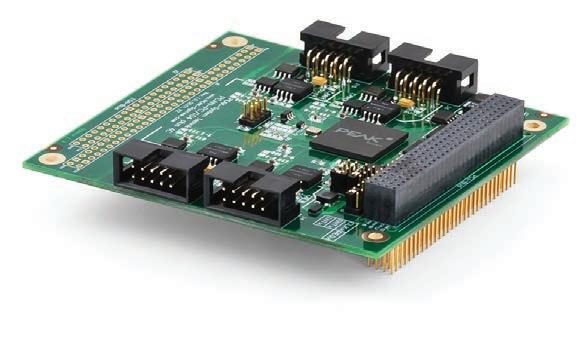
The PCAN-PCI/104-Express card enables the connection of one or two CAN buses to a PCI/104-Express system. Up to four cards can be stacked together. The CAN bus is connected using a 9-pin D-Sub plug on the slot brackets supplied. There is galvanic isolation of up to 500 Volts between the computer and CAN sides.
The package is also supplied with the CAN monitor PCAN-View for Windows and the programming interface PCAN-Basic.


FEATURES:
Ą PCI/104-Express card, 1 lane (x1)
Ą Form factor PC/104
Ą Up to four cards can be used in one system
Ą 1, 2, or 4 High-speed CAN channels (ISO 11898-2)
Ą Complies with CAN specifications 2.0 A/B and FD (ISO and Non-ISO)
Ą CAN FD bit rates for the data field (64 bytes max.) from 20 kbit/s up to 12 Mbit/s
Ą CAN bit rates from 20 kbit/s up to 1 Mbit/s
Ą Connection to CAN bus through D-Sub slot bracket, 9-pin (in accordance with CiA® 106)
Ą FPGA implementation of the CAN FD controller
Ą Microchip CAN transceiver MCP2558FD
Ą Galvanic isolation on the CAN connection up to 500 V, separate for each CAN channel
Ą CAN termination and 5-Volt supply to the CAN connection can be activated through a solder jumper
Ą Extended operating temperature range from -40 to +85 °C (-40 to +185 °F)
Ą Optionally available: PCI-104 stack-through connector
PEAK-System Technik GmbH
www.peak-system.com/quick/PC104-5

The PCAN-PCI/104-Express FD allows the connection of PCI/104Express systems to CAN and CAN FD buses. Up to four cards can be stacked together. The CAN bus is connected via 9-pin D-Sub connectors to the supplied slot brackets. There is a galvanic isolation between the computer and the CAN side up to 500 Volts. The card is available as a single, dual, or four-channel version. The monitor software PCAN-View and the programming interface PCAN-Basic are included in the scope of supply and support the standard CAN FD.
As devices become more connected, networks become more congested. The AIROC™ CYW55573, Wi-Fi 6/6E tri-band 2x2 Wi-Fi and Bluetooth® 5.3 SoC, solves these issues by surpassing the Wi-Fi 6/6E standards. It supports tri-band (2.4G, 5G, 6G), and improves range, power efficiency, network robustness and security, while reducing total Bill of Materials cost and board space.
The solution also delivers exceptional high-quality video/audio streaming and seamless connectivity experience in congested network environments and significantly reduces latency by operating in the 6G spectrum. It is ideal for video, audio, industrial and commercial applications such as surveillance cameras, wireless speakers, home entertainment, Indoor/ warehouse asset tracking hubs, mobile PoS, and more.
Ą Wi-Fi 6/6E, tri-band, 2x2 MIMO, release 1 and 2 features: OFDMA, MU-MIMO, TWT, DCM
Ą 20/40/80 MHz channels, 1024-QAM, up to 1.2 Gbps PHY data rate
Ą AIROC™ range boost and enhanced power saving features at chip and system level
Ą Multi-layer security for protection through whole product lifecycle
Ą Smart coexistence between Wi-Fi and Bluetooth® or to external LTE, 15.4 radio
Ą Bluetooth® 5.3 certified, Dual-mode operation
Ą LE audio with Auracast™ broadcast, LE- 2Mbps, Long Range, Advertising Extensions

Apacer manufactures a variety of stable and durable industrial SSD solutions and DRAM memory modules, which are widely used in the embedded applications.

Apacer industrial SSD solutions include NVMe/ PCIe, SATA, PATA, Card, and USB interfaces. Form factors cover 2.5”, 1.8”, M.2, MO-300, MO-300B, MO-297, MO-276, 7-Pin Module, CF, CFast, CFexpress, SD, microSD, USB Flash Drive, and USB Flash module.
Apacer DRAM memory modules for embedded applications include DDR5, DDR4, DDR3, DDR2 and DDR in the type of DIMM, SODIMM, ECC DIMM, and ECC SODIMM.
Ą Anti-Sulfuration, the world’s first patented anti-sulfuration memory modules and anti-sulfuration SSDs with the industry’s highest level of anti-corrosion certification can meet the needs of industrial products facing harsh environments. Apacer's patented Anti-Sulfuration Memory Modules use special alloy materials as passive components, which have passed the ASTM B809-95 anti-sulfuration test. Apacer's Anti-Sulfuration SSDs Passed ANSI/ISA 71.04 G3 Certification.
Ą Wide Temperature, Apacer’s products are designed with wide temperature support to ensure operation reliability in extreme temperatures ranging from -40° C to 85° C. Apacer’s wide-temp series of products, including memory chips, passive elements, and PCB, are all full-scale industrial grade. These products have passed industrial extended temperature tests and the most extreme thermal cycling test, ensuring their quality, reliability, and durability.
NexAIoT’s new NIFE 210 factory automation fanless system with fieldbus expansion ability is designed for industrial and factory automation, including real-time monitoring, data management, and remote control. With onboard quad-core Intel® Celeron® processor J6413 (Elkhart Lake) operating at 1.8 GHz, NIFE 210 delivers high-performance data processing with minimal power consumption for edge and control applications. The NIFE 210 supports up to 32 GB SO-DIMM DDR4.
The NIFE 210 features front access to all interfaces to support simple wiring, rapid deployment, and plug-and-play functionality. The NIFE 210 offers flexible connectivity options and elevated efficiency and security through one 2.5Gbe and two 1Gbe network interfaces while offering more connectivity options with two USB 3.0, four USB 2.0 connectors, two isolated COM ports with auto-flow control, and support for dual independent display DP++ and HDMI.
On the data backup side, the NIFE 210 offers several storage options – front access 2.5″ SATA SSD/HDD bay that supports a combo storage solution combining 2.5” SSD & Micro SD cards in one module, internal 2.5″ SATA SSD/HDD bay (Only NIFE 210-E11), and mSATA storage.
Two mini PCIe slots and M.2 3042/3052 B key provide the NIFE 210 with wireless communication capabilities such as BT/Wi-Fi, and 5G/4G LTE. To realize factory-wide automation, the NIFE 210 supports fieldbus modules including PROFIBUS®, PROFINET®, DeviceNet®, CANopen® , SERCOS® III, EtherNet/IP®, and EtherCAT® master. Connection to peripherals and sensors can also be established with COM, USB, and optional GPIO ports. NIFE 210 has onboard TPM 2.0.
Aimed at industrial environments as well as incabinet installations with limited space, the NIFE 210 features a fanless design, versatile installation methods including DIN-rail, wall and stand mount, supports 24V DC input with ±20% range, -10 ~ 60 °C/ 14 ~ 140 °F operating temperature, and EMI protection for use in electronic noise-prone industrial environments.
Ą Ideal for a variety of industrial applications ranging from CNC automation, edge computing, machine automation, and control cabinet
Ą Onboard Intel® Celeron® processor J6413 Quad Core 1.8GHz
Ą Flexible data storage 2.5” SATA HDD/SSD, support ComboStorage (2.5” SSD + MicroSD card), mSATA
Ą 1 x DP++ and 1 x HDMI for dual independent display support
Ą 1 x Intel® 2,5GbE LAN port (support WoL & PXE), 2 x Marvell PHY GbE LAN ports (support WoL)
Ą 2 x RS232/422/485 with auto-flow control and 2.5KV isolation protection, 2 x USB 3.0, 4 x USB 2.0
Ą 2 x Mini-PCIe, 1 x M.2 3042/3052 B key, and PCIE x4 expansion in selected SKUs
Ą Fieldbus connectivity: PROFIBUS®, PROFINET®, DeviceNet® , CANopen®, SERCOS® III, EtherNet/IP®, and EtherCAT® master
Ą Simplified programming with CODESYS Control RTE and CODESYS SoftMotion tool kit
Ą Onboard TPM2.0 for enhanced cyber security
Ą Long-term product availability
Our batteries offer a winning combination: a patented hybrid layer capacitor (HLC) that delivers the high pulses required for two-way wireless communications; the widest temperature range of all; and the lowest self-discharge rate (0.7% per year), enabling our cells to last up to 4 times longer than the competition.
Looking to have your remote wireless device complete a 40-year marathon? Then team up with Tadiran batteries that last a lifetime.
