
11 minute read
DfAM
Design for Additive Manufacturing
3D-printed circuit boards: How they’re made and why they matter
Once confi ned mainly to home-brew tinkering, circuit boards created via 3D printing are now practical for some manufactured products.
J.F. Brandon • BotFactory Inc.

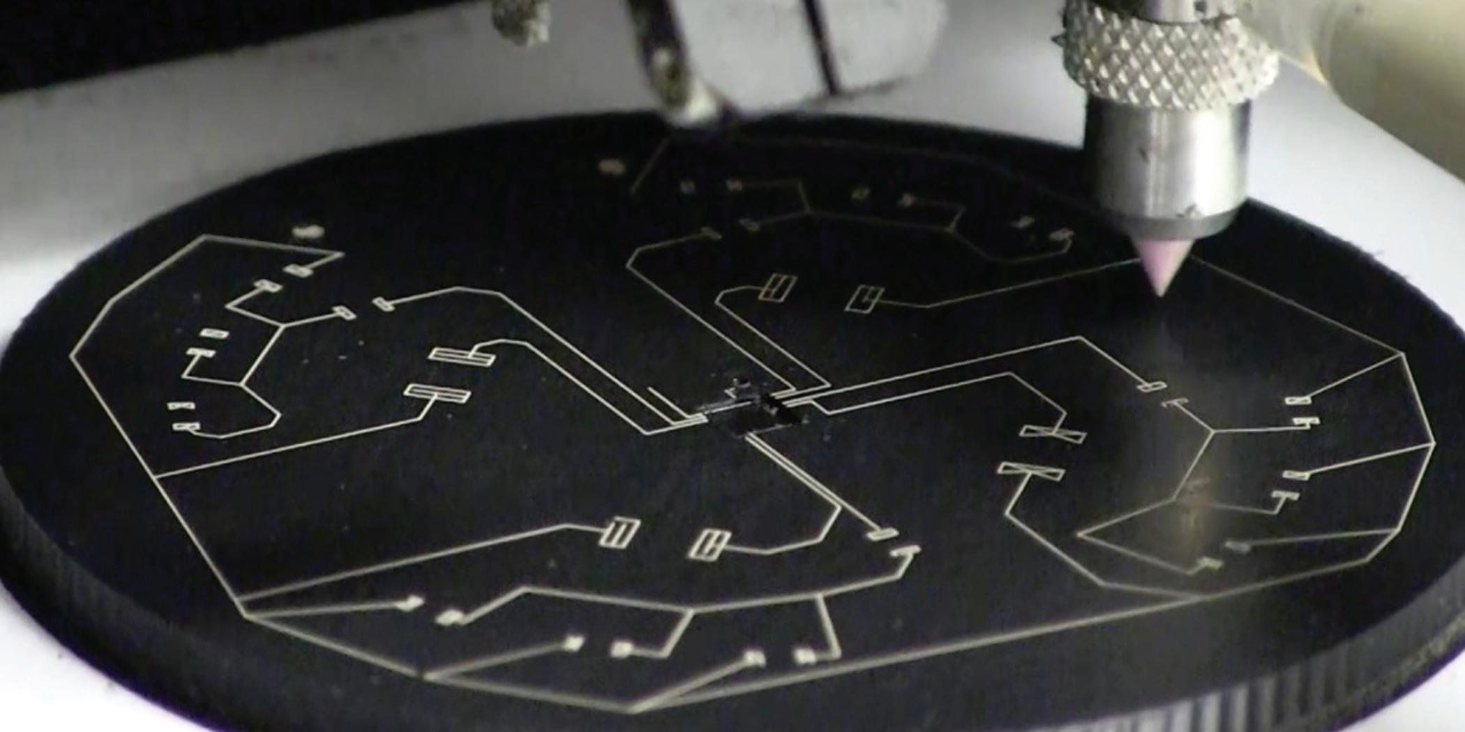
Example of an nScrypt system extruding conductive traces on a FDM-printed substrate.
In the past ten years 3D Printing has gone om a niche prototyping tool to a process acceptable for mass production. Most of the recent hubbub has been about monolithic plastic and metals. But new materials and processes have appeared to help create 3D-printed PCBs that meet long-standing engineering problems. If the history of electronics manufacturing could be summarized in one phase, it would be, “Shrinking everything to nothing to squeeze out something faster.” The push towards miniaturization has been driven by the inviolable laws of nature – faster devices that consume less power require shorter electrical paths. However, the printed circuit board is an outlier in the electronics world. PCBs still use basic drilling and plating processes perfected 50 years ago. That is not to say that PCB manufacturing is trivial or antiquated. But the investment in new PCB manufacturing methods is a pittance compared to the hundreds of billions put into chip fabs by IC makers such as TMSC and AMD. It is worth looking at the details of PCBs and their construction. The word ‘printed’ in printed circuit board only describes half of the process – the silkscreen masks are the only part that is printed. A PCB is originally copper foil on a rigid fi berglass laminate which is selectively etched, drilled, and plated using a set of silkscreens and chemical baths to produce the fi nal product. The sole purpose of the PCB is to reliably connect passive and active components and provide a reliable platform for integration or interactions with the rest of a product. For example, the PCB in the average computer keyboard connects electronic elements together, and manages human interactions and provides a sound mechanical connection to
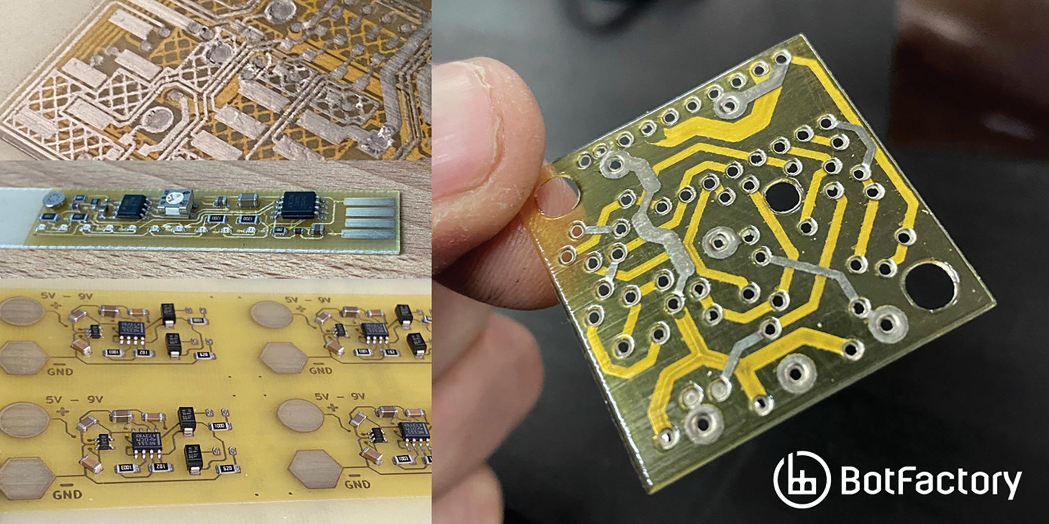
Examples of inkjet-printed circuitry made with a BotFactory SV2 PCB printer.
the body of the product. PCBs must be designed so they can easily be stenciled with reflow solder paste and integrated into industrial surface-mount pick-andplace lines. All in all, modern PCBs can play a variety of roles in the end products. So it is worth considering new manufacturing processes that can expand the capabilities of PCBs.
PCBs have thermal, electrical, geometric and mechanical requirements that go beyond what most materials for 3D printing can offer. For example, the average $500 3D printer that uses Fused Deposition Modeling (FDM) uses PLA, ABS and PETG which melt under the harsh gaze of any standard soldering station. Metal 3D printing techniques handle one material at one time. Yet PCBs require, at a bare minimum, a dense and conductive metal for conductors.
Three technical paths have appeared for PCB printing: inkjets, extrusion, and additive manufacturing (AM)-electroless plating. First consider inkjetting. New nanoparticle and particle-free inks have allowed inkjet printing to go beyond CMYK inks and graphics. Inkjets can now lay down metal (overwhelmingly silver) inks in fine patterns on flexible materials. In combination with a polymer ink, it is possible to create PCBs with complex multilayer circuitry (blind and buried vias are trivial items) in only a few steps on a single machine.
The inherent advantage of creating PCBs layer-by-layer this way is that each layer can be tested and validated. The minimal level of processing simplifies the dispensing solder paste, part assembly, and testing for every layer. The disadvantages are that material dispensing via inkjet printing is slow relative to all other additive manufacturing processes-- deposition speeds can be in the millimeters-perhour range. It’s possible to create precise traces with inkjet printing (metal traces with 100-micron widths are commonly attainable). But the smaller droplets limit deposition speeds.
And there are problems with metal inks: Applying too much can cause bleeding and cracking during drying, thus limiting PCB fabrication speeds. Solderability is a particular blind spot – silver can wilt under standard pastes like SAC305, suffering from tin ‘scavenging’ silver during reflow. In addition, inkjet polymers melt at temperatures that standard PCBs easily manage. Fortunately, industry-accepted lowtemperature tin-bismuth and indiumbased solder pastes are compatible with inkjet-printed PCBs.
Today there are two PCB printers that use inkjetting – the BotFactory SV2 and the Nano Dimension DragonFly. Each printer uses the same process to create multilayer circuitry, although the BotFactory SV2 uses inexpensive thermal inkjet heads instead of the piezo heads found in the DragonFly. Nano Dimension has focused on printing for production, whereas BotFactory has emphasized integration of pasting and PCB assembly into a small unit, working on projects with the USAF to automate the entire process. BotFactory offers a commercial product below $20,000.
Single nozzle jetting Inkjetting isn’t the only way that nanoparticles can be deposited to create circuitry. An alternative method extrudes lines onto flat surfaces and uses fused-deposition modeling to provide a polymer structure for the traces to inhabit. Pastes are notoriously difficult to control when creating fine traces and spaces, requiring precise control and extremely close contact with the substrate surface.
Here the target surface must be covered twice – first for mapping, then for pasting. The two-step procedure handicaps the scalability of the process for production. Pastes must be devoid of air pockets lest each bubble act as a kind of ‘spring’ and impede the extrusion process. The flip side of using viscous pastes is that metal-loading is higher and it’s possible to deposit metal in thicker layers, boosting conductivity and solderability. However, at
Design for Additive Manufacturing

this time, silver is the favorite material and suff ers om the same constraints as inkjetprinted PCBs in regards to silver scavenging. AM + electroless plating (also abbreviated as AMEP, or 3D-Print-andPlate) is a completely new category of AM that combines existing additive manufacturing processes and wellunderstood electroless plating techniques. An object is printed via stereolithography (SL) or FDM using a distinct metal-loaded material that can be electroless-plated a erwards. AMEP continues to be a topic of academic research. Last year, researchers at UCLA published results on using SL to create multi-material prints that could be selectively plated. Using two vats of pure and metal-loaded polymers, the process enhances the existing premise of AM with no extra constraint on fabrication speed. Palladium, a metal traditionally extremely expensive, normally serves as a seed material in this process. But on the other side of the world, UK researchers devised a way of printing less expensive metal on a new polyimide material. Polyimide (also known as Kapton) is prized by electrical engineers in fl exible and printed electronics for its low thermal expansion and dielectric constant. UK researchers found UV energy can be used to chemically bond silver particles and the polymer chains, providing seeds for plating a erwards. The technology described above has not been commercialized, but the overall concept has been used for creating unique antennae at fi rms like Swissto12. There a high-resolution SL print is made, coated, and then electro-plated (not electroless plated). Electroplating requires a current to initiate and control the plating process, whereas a PCB o en has unconnected traces and vias that require plating. Overall, the greatest challenge to AMEP is that it cannot create conductors within an object unless there are exposed holes or the PCB undergoes multiple dips into the plating baths. As it stands, the technology has the ability to meet all the technical requirements for highperformance PCBs, including ease-ofsolderability and high-thermal tolerances.
What it’s not There is some confusion about what is and isn’t ‘AM electronics,’ and certain lines have been drawn. Any process that builds circuitry on pre-existing substrates or augments AM with subtractive processes is not 3D-printed electronics. By conveniently ignoring the drilling process for vias and shaping, one could argue that PCBs are made with AM when they clearly are not. When an entire model is fabricated using AM, it typically has characteristics and form factors that go beyond what would be possible if subtractive fabrication is included. Use of subtractive processes detracts om the entire point of adopting AM. An example of semi-additive process commonly cited as 3D-printed electronics is Laser Directed Structuring developed by LPKF. Essentially, an object consists of an injection-molded plastic that has been fi lled or coated by an organometallic compound. When a laser applies a circuit pattern to the surface, metallic seeds form and create an electroless nickel or copper plating. The technology is limited by the reach of the laser, inhibiting the possibility of allowing conductors to pass thru the object. Thus LDS parts are not true 3D PCBs. The same limitation also applies to aerosol jetting, a concept commercialized by Optomec. Here a carrier gas (nitrogen typically) jets out of a fi ne nozzle at high speed and carries a fi ne suspension of materials such as nanoparticle metal inks. The variety of viscosity, metal-loading and material choice makes aerosol jetting a candidate for creating sensors on objects, overcoming the limited choice of materials for LDS. As both processes use non-AM elements, they arguably do not create 3D-printed electronic devices. Credible advances in materials, metals and polymers make it possible to 3D-print PCBs useful in many applications today. The most mature technique is inkjet printing; it comes closest to reaching the necessary geometric and electric properties, with materials advancing quickly to meet the thermal and mechanical needs. Extrusion is well-understood but hard to scale. AM-EP is the dark horse in the race, combining old and new techniques to provide another path to the 3D PCB. DW
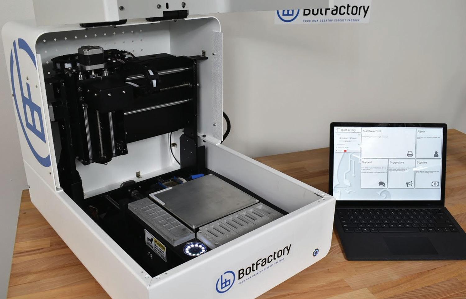
The BotFactory SV2 is capabile of printing PCBs and utilizes inexpensive thermal inkjet heads. BotFactory Inc. | www.botfactory.co
Design for Additive Manufacturing

Three new 3D printers om Stratasys encompass FDM, P3, and SAF technologies
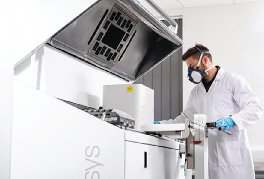
Stratasys Ltd., recently introduced three new 3D printers to address a large portion of the multibillion-dollar additive manufacturing of end-use parts market. The systems collectively are aimed at accelerating the shi om traditional to additive manufacturing for low-to-mid-volume production applications underserved by traditional manufacturing methods. The Stratasys H350 3D printer can produce thousands of parts. Powered by SAF technology, this printer is designed to give manufacturers production consistency, a competitive and predictable cost per part, and complete control for the production of thousands of parts. The H350 printer includes about a dozen diff erent parts 3D-printed with SAF technology. The H350 printer has been in beta testing since early 2021 with service bureaus and contract manufacturers in Europe, Israel, and the United States, including Stratasys Direct Manufacturing, which is now selling parts on demand using the system. It is expected to ship more broadly to customers in Q3 of this year. Applications include end-use parts such as covers, connectors, hinges, cable holders, electronics housings, and ducting. Stratasys is using certifi ed third-party materials for H Series systems. The initial material is Stratasys High Yield PA11, which is a bio-based plastic made om sustainable castor oil. The Stratasys Origin One brings production scale 3D printing for detailed and intricate parts. Coming om the acquisition of Origin, this 3D printer uses proprietary P3 technology and a so warefi rst architecture to produce parts at volume in a range of open, certifi ed third-party materials with industry-leading accuracy, detail, fi nish, repeatability, and time to part. Internal Stratasys estimates suggest a $3.7 billion market opportunity by 2025 for the production-oriented segments suited to the Origin One, including automotive, consumer goods, medical, dental, and tooling applications. The third new system announced was the Stratasys F770 3D printer. For big parts, Stratasys claims this newest FDM 3D printer features the “longest fully heated build chamber on the market and a generous build volume of over 13 cubic feet (372 liters).” The new system, priced under $100,000, is for prototyping, jigs and fi xtures, and tooling applications requiring standard thermoplastics. Soluble support material simplifi es post processing, while GrabCAD Print so ware streamlines workfl ow and enterprise connectivity is enabled through the MTConnect standard and the GrabCAD SDK. DW
Stratasys | www.stratasys.com
Desktop Metal qualifies another material for its additive systems— 316L stainless steel
Known for its corrosion resistance and excellent mechanical properties at extreme temperatures, 316L stainless steel is well suited for applications in demanding conditions, such as parts exposed to marine or pharmaceutical processing environments, food preparation equipment, medical devices and surgical tooling. It also exhibits excellent weldability by standard fusion and resistance methods.
Through extensive testing, the Desktop Metal materials science team has validated that 316L stainless steel printed on Production System technology and sintered by Desktop Metal meets MPIF 35 standards for structural powder metallurgy parts set by the Metal Powder Industries Federation. Parts printed with 316L have demonstrated excellent mechanical properties and corrosion resistance, while significantly decreasing production time and part cost.
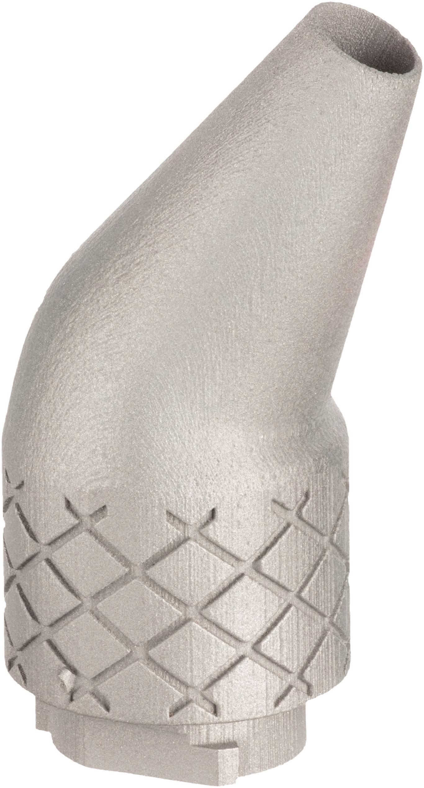
Because 316L is a surgical-grade steel, it is an ideal material for medical applications like surgical nozzles. By eliminating tooling, additive manufacturing enables mass production runs of different sized nozzles with no lead time, featuring internal channels that are optimized for individual patient needs.
Printing on the Production System P-50 eliminates multiple fixturing steps otherwise required for machining, and results in a throughput of more than 24,000 parts per week at approximately $2.50 per part. By comparison, machining the same part would cost $20.00 -$40.00 per part, and require up to two months to create the same number of parts the P-50 can produce in just one week. DW
Desktop Metal www.desktopmetal.com


